


INTEGRATED CIRCUITS
DATA SH EET
SAA4994H
Field and line rate converter
with noise reduction
Product specification
File under Integrated Circuits, IC02
2001 Nov 23

Philips Semiconductors Product specification
Field and line rate converter
with noise reduction
CONTENTS
1 FEATURES
2 GENERAL DESCRIPTION
2.1 Patent notice
3 QUICK REFERENCE DATA
4 ORDERING INFORMATION
5 BLOCK DIAGRAMS
6 PINNING
7 FUNCTIONAL DESCRIPTION
8 CONTROL REGISTER DESCRIPTION
9 LIMITING VALUES
10 THERMAL CHARACTERISTICS
11 CHARACTERISTICS
SAA4994H
12 PACKAGE OUTLINE
13 SOLDERING
13.1 Introduction to soldering surface mount
packages
13.2 Reflow soldering
13.3 Wave soldering
13.4 Manual soldering
13.5 Suitability of surface mount IC packages for
wave and reflow soldering methods
14 DATA SHEET STATUS
15 DEFINITIONS
16 DISCLAIMERS
2001 Nov 23 2

Philips Semiconductors Product specification
Field and line rate converter
with noise reduction
1 FEATURES
• Upconversion of all 1fH film and video standards up to
292 active input lines per field
• 100/120 Hz 2 : 1, 50/60 Hz 1 : 1 and 100/120 Hz 1 : 1
output formats
• 4:1:1, 4:2:2 and 4 : 2 : 2 Differential Pulse Code
Modulation (DPCM) input colour formats; 4 :1:1 and
4:2:2 output colour formats
• Full 8-bit accuracy
• Improved recursive de-interlacing
• Film (25 and 30 Hz) upconversion to 100/120
movement phases per second
• Variable vertical sharpness enhancement
• Motion compensated 3D dynamic noise reduction
• High quality vertical zoom
• 2 Mbaud serial interface (SNERT)
• Software andpin-to-pin compatible to SAA4992H (uses
3.3 V power supply) and SAA4993H
• Demonstration mode for noise reduction, motion
compensation and colour overlay.
SAA4994H
2 GENERAL DESCRIPTION
The SAA4994H is a completely digital monolithic
integrated circuit which can be used for field and line rate
conversion of all global TV standards.
It features improved Natural Motion
It can be configured to emulate the SAA4990H as well as
the SAA4991WP. For demonstration purposes a split
screen mode to show the Dynamic Noise Reduction
(DNR) function and natural motion is available and a
colour vector overlay mode exists.
The SAA4994H supports a Boundary Scan Test (BST)
circuit in accordance with IEEE 1149.
2.1 Patent notice
Notice is herewith given that the subject integrated circuit
uses one or more of the following US patents and that
each of these patents may have corresponding patents in
other jurisdictions.
US 4740842, US 5929919, US 6034734, US 5534946,
US 5532750, US 5495300, US 5903680, US 5365280,
US 5148269, US 5072293, US 5771074, and
US 5302909.
(1)
performance.
(1) Natural Motion is a trademark of Koninklijke Philips
Electronics N.V.
3 QUICK REFERENCE DATA
SYMBOL PARAMETER MIN. TYP. MAX. UNIT
V
DDI
V
DDE
I
DD
f
CLK32
T
amb
core supply voltage 2.3 2.5 2.7 V
external supply voltage (output pads) 3.0 3.3 3.6 V
supply current − 280 − mA
operating clock frequency − 32 33.3 MHz
ambient temperature 0 − 70 °C
4 ORDERING INFORMATION
TYPE
NUMBER
NAME DESCRIPTION VERSION
SAA4994H QFP160 plastic quad flat package; 160 leads (lead length 1.6 mm);
PACKAGE
SOT322-2
body 28 × 28 × 3.4 mm; high stand-off height
2001 Nov 23 3
This text is here in white to force landscape pages to be rotated correctly when browsing through the pdf in the Acrobat reader.This text is here in
_white to force landscape pages to be rotated correctly when browsing through the pdf in the Acrobat reader.This text is here inThis text is here in
white to force landscape pages to be rotated correctly when browsing through the pdf in the Acrobat reader. white to force landscape pages to be ...
2001 Nov 23 4
FIELD MEMORY 2
handbook, full pagewidth
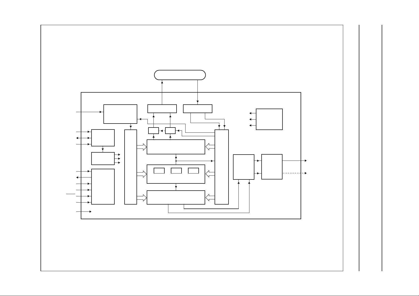
5 BLOCK DIAGRAMS
Philips Semiconductors Product specification
Field and line rate converter
with noise reduction
YA0 to YA7
SNCL
SNDA
SNRST
TCK
TDO
TDI
TMS
TRST
TE
CLK32
45 to 52
27
26
25
35
34
33
32
31
30
79
SNERT
INTERFACE
CONTROL
BST/TEST
DYNAMIC
NOISE
REDUCTION
MPR
LEFT
YB7 to YB0
151, 152,
154 to 159
COMPRESS
MUX
MUX
DE-INTERLACER
vectors
SPM TPM ESM
MOTION ESTIMATOR
vectors
UPCONVERSION
YC0 to YC7
2 to 9
DECOMPRESS
MPR
RIGHT
VERTICAL
PEAKING
SEQUENCER
SAA4994H
VERTICAL
ZOOM
61 to 68
82 to 89
MHC059
YF7 to YF0
YG7 to YG0
SAA4994H
The solid lines represent pixel data; the broken lines represent controls.
Fig.1 Block diagram of the luminance part.
This text is here in white to force landscape pages to be rotated correctly when browsing through the pdf in the Acrobat reader.This text is here in
_white to force landscape pages to be rotated correctly when browsing through the pdf in the Acrobat reader.This text is here inThis text is here in
white to force landscape pages to be rotated correctly when browsing through the pdf in the Acrobat reader. white to force landscape pages to be ...
2001 Nov 23 5
FIELD MEMORY 2
handbook, full pagewidth
Philips Semiconductors Product specification
Field and line rate converter
with noise reduction
UVA0 to UVA7
37 to 44
DECOMPRESS/
REFORMAT
DNR
MPR
LEFT
UVB3 to UVB0
147 to 150
COMPRESS/
FORMAT
UPCONVERSION
vectors
UVC0 to UVC3
10 to 13
DECOMPRESS/
REFORMAT
MPR
RIGHT
SAA4994H
VERTICAL
ZOOM
FORMAT
70 to 77
91 to 98
MHC060
UVF7 to YVF0
UVG7 to YVG0
SAA4994H
The solid lines represent pixel data; the broken lines represent controls.
Fig.2 Block diagram of the chrominance part.

Philips Semiconductors Product specification
Field and line rate converter
SAA4994H
with noise reduction
6 PINNING
SYMBOL PIN TYPE DESCRIPTION
V
SSE
1 ground ground of output pads
YC0 2 input bus C luminance input from field memory 2 bit 0 (LSB)
YC1 3 input bus C luminance input from field memory 2 bit 1
YC2 4 input bus C luminance input from field memory 2 bit 2
YC3 5 input bus C luminance input from field memory 2 bit 3
YC4 6 input bus C luminance input from field memory 2 bit 4
YC5 7 input bus C luminance input from field memory 2 bit 5
YC6 8 input bus C luminance input from field memory 2 bit 6
YC7 9 input bus C luminance input from field memory 2 bit 7 (MSB)
UVC0 10 input bus C chrominance input from field memory 2 bit 0 (LSB)
UVC1 11 input bus C chrominance input from field memory 2 bit 1
UVC2 12 input bus C chrominance input from field memory 2 bit 2
UVC3 13 input bus C chrominance input from field memory 2 bit 3 (MSB)
REC 14 output read enable output for busC
V
V
V
V
SSE
DDE
SSI
DDI
15 ground ground of output pads
16 supply external supply voltage (output pads)
17 ground core ground
18 supply core supply voltage
JUMP0 19 input configuration pin 0; will be stored in register 0B3 e.g. to indicate presence of 3rd field
memory; should be connected to ground or to V
JUMP1 20 input configuration pin 1; will be stored in register 0B5 e.g. to indicate presence of 16-bit
1st field memory for full 4:2:2;should be connected to ground or to V
resistor of 47 kΩ
V
V
V
DDE
DDI
SSI
21 supply external supply voltage (output pads)
22 supply core supply voltage
23 ground core ground
RAMTST1 24 input test pin 1 input for internal RAM testing with internal pull-down; connect to ground for
normal operation
SNRST 25 input SNERT bus reset input
SNDA 26 I/O SNERT bus data input and output
SNCL 27 input SNERT bus clock input
V
SSE
28 ground ground of output pads
RAMTST2 29 input test pin 2 input for internal RAM testing with internal pull-down; connect to ground for
normal operation
TE 30 input test mode input with internal pull-down; if not used it has to be connected to ground
TRST 31 input boundary scan test reset input (active LOW); if not used it has to be connected to V
via a pull-up resistor of 47 kΩ
TMS 32 input boundary scan test mode select input; if not used it has to be connected to V
pull-up resistor of 47 kΩ
TDI 33 input boundary scan test data input; if not used it has to be connected to V
resistor of 47 kΩ
(1)(2)
via a pull-up resistor of 47 kΩ
DDE
DDE
DDE
via a pull-up
via a
DDE
via a pull-up
DDE
2001 Nov 23 6

Philips Semiconductors Product specification
Field and line rate converter
with noise reduction
SYMBOL PIN TYPE DESCRIPTION
TDO 34 3-state boundary scan test: data output
TCK 35 input boundary scan test: clock input; if not used it has to be connected to V
resistor of 47 kΩ
V
SSE
36 ground ground of output pads
UVA0 37 input bus A chrominance input from field memory 1 bit 0 (LSB)
UVA1 38 input bus A chrominance input from field memory 1 bit 1
UVA2 39 input bus A chrominance input from field memory 1 bit 2
UVA3 40 input bus A chrominance input from field memory 1 bit 3
UVA4 41 input bus A chrominance input from field memory 1 bit 4
UVA5 42 input bus A chrominance input from field memory 1 bit 5
UVA6 43 input bus A chrominance input from field memory 1 bit 6
UVA7 44 input bus A chrominance input from field memory 1 bit 7 (MSB)
YA0 45 input bus A luminance input from field memory 1 bit 0 (LSB)
YA1 46 input bus A luminance input from field memory 1 bit 1
YA2 47 input bus A luminance input from field memory 1 bit 2
YA3 48 input bus A luminance input from field memory 1 bit 3
YA4 49 input bus A luminance input from field memory 1 bit 4
YA5 50 input bus A luminance input from field memory 1 bit 5
YA6 51 input bus A luminance input from field memory 1 bit 6
YA7 52 input bus A luminance input from field memory 1 bit 7 (MSB)
REA 53 output read enable output for bus A
V
V
V
V
V
V
SSE
SSI
DDI
DDI
SSI
SSE
54 ground ground of output pads
55 ground core ground
56 supply core supply voltage
57 supply core supply voltage
58 ground core ground
59 ground ground of output pads
REF 60 input read enable input for bus F and G
YF7 61 output bus F luminance output bit 7 (MSB)
YF6 62 output bus F luminance output bit 6
YF5 63 output bus F luminance output bit 5
YF4 64 output bus F luminance output bit 4
YF3 65 output bus F luminance output bit 3
YF2 66 output bus F luminance output bit 2
YF1 67 output bus F luminance output bit 1
YF0 68 output bus F luminance output bit 0 (LSB)
V
DDE
69 supply external supply voltage (output pads)
UVF7 70 output bus F chrominance output bit 7 (MSB)
UVF6 71 output bus F chrominance output bit 6
UVF5 72 output bus F chrominance output bit 5
UVF4 73 output bus F chrominance output bit 4
(1)(2)
SAA4994H
via a pull-up
DDE
2001 Nov 23 7

Philips Semiconductors Product specification
Field and line rate converter
with noise reduction
SYMBOL PIN TYPE DESCRIPTION
UVF3 74 output bus F chrominance output bit 3
UVF2 75 output bus F chrominance output bit 2
UVF1 76 output bus F chrominance output bit 1
UVF0 77 output bus F chrominance output bit 0 (LSB)
V
SSE
78 ground ground of output pads
CLK32 79 input system clock input
V
V
SSI
SSE
80 ground core ground
81 ground ground of output pads
YG7 82 3-state bus G luminance output bit 7 (MSB)
YG6 83 3-state bus G luminance output bit 6
YG5 84 3-state bus G luminance output bit 5
YG4 85 3-state bus G luminance output bit 4
YG3 86 3-state bus G luminance output bit 3
YG2 87 3-state bus G luminance output bit 2
YG1 88 3-state bus G luminance output bit 1
YG0 89 3-state bus G luminance output bit 0 (LSB)
V
DDE
90 supply external supply voltage (output pads)
UVG7 91 3-state bus G chrominance output bit 7 (MSB) or vector output bit 7
UVG6 92 3-state bus G chrominance output bit 6 or vector output bit 6
UVG5 93 3-state bus G chrominance output bit 5 or vector output bit 5
UVG4 94 3-state bus G chrominance output bit 4 or vector output bit 4
UVG3 95 3-state bus G chrominance output bit 3 or vector output bit 3
UVG2 96 3-state bus G chrominance output bit 2 or vector output bit 2
UVG1 97 3-state bus G chrominance output bit 1 or vector output bit 1
UVG0 98 3-state bus G chrominance output bit 0 (LSB) or vector output bit 0
V
V
V
V
V
V
V
SSE
SSI
DDI
DDE
DDI
SSI
SSE
99 ground ground of output pads
100 ground core ground
101 supply core supply voltage
102 supply external supply voltage (output pads)
103 supply core supply voltage
104 ground core ground
105 ground ground of output pads
n.c. 106 − not connected
TSTO1 107 output test output 1
TSTO2 108 output test output 2
TSTO3 109 output test output 3
TSTO4 110 output test output 4
TSTO5 111 output test output 5
TSTO6 112 output test output 6
V
DDE
113 supply external supply voltage (output pads)
TSTO7 114 output test output 7
(1)(2)
SAA4994H
2001 Nov 23 8

Philips Semiconductors Product specification
Field and line rate converter
SAA4994H
with noise reduction
SYMBOL PIN TYPE DESCRIPTION
TSTO8 115 output test output 8
TSTO9 116 output test output 9
TSTO10 117 output test output 10
TSTO11 118 output test output 11
TSTO12 119 output test output 12
V
V
SSE
SSE
120 ground ground of output pads
121 ground ground of output pads
TSTI1 122 input test input 1
TSTI2 123 input test input 2
TSTI3 124 input test input 3
TSTI4 125 input test input 4
TSTI5 126 input test input 5
TSTI6 127 input test input 6
TSTI7 128 input test input 7
TSTI8 129 input test input 8
TSTI9 130 input test input 9
TSTI10 131 input test input 10
TSTI11 132 input test input 11
TSTI12 133 input test input 12
TSTO13 134 output test output 13
V
SSE
135 ground ground of output pads
HREF 136 input horizontal reference synchronization input
V
SSI
V
DDI
137 ground core ground
138 supply core supply voltage
OSCI 139 input test pin with internal pull-down; connect to ground for normal operation
RESFM 140 output reset field memory output for pin OSCI = LOW or test output OSCOUT for
pin OSCI = HIGH
V
V
V
DDE
DDI
SSI
141 supply external supply voltage (output pads)
142 supply core supply voltage
143 ground core ground
ACV 144 output active video output
V
SSE
145 ground ground of output pads
WEB 146 output write enable output for bus B
UVB3 147 output bus B chrominance output to field memory 2 bit 3 (MSB)
UVB2 148 output bus B chrominance output to field memory 2 bit 2
UVB1 149 output bus B chrominance output to field memory 2 bit 1
UVB0 150 output bus B chrominance output to field memory 2 bit 0 (LSB)
YB7 151 output bus B luminance output to field memory 2 bit 7 (MSB)
YB6 152 output bus B luminance output to field memory 2 bit 6
V
DDE
153 supply external supply voltage (output pads)
YB5 154 output bus B luminance output to field memory 2 bit 5
(1)(2)
2001 Nov 23 9

Philips Semiconductors Product specification
Field and line rate converter
SAA4994H
with noise reduction
SYMBOL PIN TYPE DESCRIPTION
YB4 155 output bus B luminance output to field memory 2 bit 4
YB3 156 output bus B luminance output to field memory 2 bit 3
YB2 157 output bus B luminance output to field memory 2 bit 2
YB1 158 output bus B luminance output to field memory 2 bit 1
YB0 159 output bus B luminance output to field memory 2 bit 0 (LSB)
V
SSE
Notes
1. Not used input pins should be connected to ground.
2. Because of the noisy characteristic of the output pad supply it is recommended not to connect the core supply and
the output pad supply directly at the device. The output pad supply should be buffered as close as possible to the
device.
160 ground ground of output pads
(1)(2)
2001 Nov 23 10

Philips Semiconductors Product specification
Field and line rate converter
with noise reduction
handbook, full pagewidth
V
SSE
YC0
YC1
YC2
YC3
YC4
YC5
YC6
YC7
UVC0
UVC1
UVC2
UVC3
REC
V
SSE
V
DDE
V
SSI
V
DDI
JUMP0
JUMP1
V
DDE
V
DDI
V
SSI
RAMTST1
SNRST
SNDA
SNCL
V
SSE
RAMTST2
TRST
TMS
TDI
TDO
TCK
V
SSE
UVA0
UVA1
UVA2
UVA3
SSE
V
YB0
YB1
YB2
160
159
158
157
1
2
3
4
5
6
7
8
9
10
11
12
13
14
15
16
17
18
19
20
21
22
23
24
25
26
27
28
29
30
TE
31
32
33
34
35
36
37
38
39
40
YB3
156
YB4
155
YB5
154
V
DDE
153
YB6
152
YB7
151
UVB0
150
UVB1
149
UVB2
148
UVB3
147
WEB
146
V
145
SSE
SSIVDDI
DDE
ACV
V
V
144
143
142
141
SAA4994H
RESFM
OSCI
140
139
DDIVSSI
V
138
137
HREF
V
136
SSE
135
TSTO13
TSTI12
134
133
TSTI11
TSTI10
132
131
TSTI9
130
TSTI8
129
TSTI7
128
TSTI6
127
TSTI5
126
SAA4994H
TSTI3
124
TSTI2
123
TSTI1
V
122
SSE
121
TSTI4
125
120
119
118
117
116
115
114
113
112
111
110
109
108
107
106
105
104
103
102
101
100
99
98
97
96
95
94
93
92
91
90
89
88
87
86
85
84
83
82
81
V
SSE
TSTO12
TSTO11
TSTO10
TSTO9
TSTO8
TSTO7
V
DDE
TSTO6
TSTO5
TSTO4
TSTO3
TSTO2
TSTO1
n.c.
V
SSE
V
SSI
V
DDI
V
DDE
V
DDI
V
SSI
V
SSE
UVG0
UVG1
UVG2
UVG3
UVG4
UVG5
UVG6
UVG7
V
DDE
YG0
YG1
YG2
YG3
YG4
YG5
YG6
YG7
V
SSE
414243444546474849505152535455565758596061626364656667686970717273747576777879
SSI
SSI
UVA4
UVA5
UVA6
UVA7
YA0
YA1
YA2
YA3
YA4
YA5
YA6
YA7
REA
V
SSE
DDIVDDI
V
SSE
V
V
V
Fig.3 Pin configuration.
2001 Nov 23 11
REF
YF7
YF6
YF5
YF4
YF3
YF2
YF1
YF0
DDE
V
UVF7
UVF6
UVF5
UVF4
UVF3
UVF2
UVF1
UVF0
V
SSE
80
V
CLK32
SSI
MHC061

Philips Semiconductors Product specification
Field and line rate converter
with noise reduction
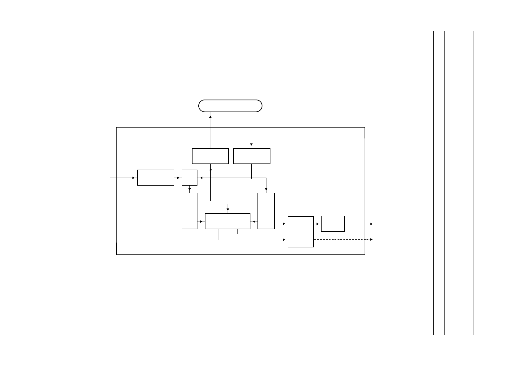
7 FUNCTIONAL DESCRIPTION
The FAL (fal_top) module builds the functional top level of
the SAA4994H. It connects the luminance data path, the
chrominance data path and the luminance
(de)compression with SAA4994H inputs and outputs as
well as controlling logic. Outside of fal_top there are only
the pad cells, boundary scan test cells, the boundary scan
test controller, the clock tree, the test enable tree and the
input port registers.
Figure 4 shows a simplified block diagram of fal_top
module. It displays the flow of pixel data (solid lines) and
controls (broken lines) between the modules inside.
Basic functionality of the modules in fal_top module is as
follows:
• KER (kernel): Y (luminance) data path
• COL (colour): UV (chrominance) data path
• YDP (Y-DPCM): compression (and decompression) of
luminance output (and input) data by Differential Pulse
Code Modulation (DPCM)
• LSE (line sequencer): generate line frequent control
signals
• SNE (interface): Synchronous No parity Eight bit
Reception and Transmission (SNERT) interface to a
microcontroller.
The SNERT interface operates in a slave receive and
transmit mode for communication with a microcontroller,
which resides on peripheral circuits (e.g. SAA4978H)
together with a SNERT master. The SNERT interface
transforms serial data from the microprocessor (via the
SNERT bus) into parallel data to be written into the
SAA4994Hs write registers and parallel data from
SAA4994Hsreadregistersinto serial data to be sent to the
microcontroller. The SNERT bus consists of 3 signals:
1. SNCL: used as serial clock signal, generated by the
master
2. SNDA: used as bidirectional data line
3. SNRST: used as a reset signal, generated by the
microcontroller to indicate the start of a transmission.
SAA4994H
Table 1 Clock cycle references
SIGNAL LATENCY
RE_F 0
RE_C 62 cycles + REceShift
YC and UVC 63 cycles
RE_A 93 cycles + REaShift
YA and UVA 94 cycles
YF, YG, UVF
and UVG
WE_B 159 cycles + 4 input lines + WEbdShift
YB and UVB 159 cycles + 4 input lines
There is an algorithmic delay of 3 lines between input and
output data. Therefore, the main data output on the
F and G bus begins while the fourth input line is read.
Writing to the B and D bus starts one input line later. The
readandwriteenablesignalsRE_A,WE_BandRE_Ccan
be shifted by control registers REaShift, WEbdShift and
REceShift, which are implemented in the line sequencer.
The fal_top module itself reads the following control
register bits (addresses):
• NrofFMs (017H)
• MatrixOn (026H) and BusGControl (028H)
• MemComp and MemDecom (026H).
NrofFMs, MatrixOn and BusGControl are used to enable
the D and G output bus, respectively. MemComp and
MemDecom are connected to YDP to control luminance
data compression and decompression. These control
register signals are not displayed in Fig.4. Further
information on the control registers is given in Chapter 8.
147 cycles + 3 input lines
The processing of a video field begins on the rising edge
of the RE_F input signal. As indicated in Fig.4, the
SAA4994H receives its inputs andgenerates its outputs at
the following clock cycles after RE_F (see Table 1).
2001 Nov 23 12

Philips Semiconductors Product specification
Field and line rate converter
with noise reduction
handbook, full pagewidth
fal_top
UVA
94 cycles
SNDA
RE_A
93 cycles
WE_B
159
cycles
RE_C
62
cycles
external field memories
UVB
159
cycles
COL
LSESNE
UVC
63
cycles
YB
159
cycles
YDP
YC
63
cycles
SAA4994H
UVF, UVG
147 cycles
RE_F
0 cycles
YA
94 cycles
The solid lines represent pixel data; the broken lines represent controls.
Fig.4 Block diagram of fal_top.
KER
YF, YG
147 cycles
MHC062
2001 Nov 23 13

This text is here in white to force landscape pages to be rotated correctly when browsing through the pdf in the Acrobat reader.This text is here in
_white to force landscape pages to be rotated correctly when browsing through the pdf in the Acrobat reader.This text is here inThis text is here in
white to force landscape pages to be rotated correctly when browsing through the pdf in the Acrobat reader. white to force landscape pages to be ...
2001 Nov 23 14
8 CONTROL REGISTER DESCRIPTION
NAME
SNERT
ADDRESS
(HEX)
READ/
WRITE
76543210 DESCRIPTION
(1)
(2)
DNR/peaking/colour
Kstep10 010 write; S
Kstep0 XXXXset LUT value: k =1⁄16 if difference below (0to15)
Kstep1 X X X X set LUT value: k =
1
⁄8 if difference below (0to15)
Kstep32 011 write; S
Kstep2 XXXXset LUT value: k =2⁄8 if difference below (0 to 30 in multiples of 2)
Kstep3 X X X X set LUT value: k =
3
⁄8 if difference below (0 to 30 in multiples of 2)
Kstep54 012 write; S
Kstep4 XXXXset LUT value: k =4⁄8 if difference below (0 to 60 in multiples of 4)
Kstep5 X X X X set LUT value: k =
5
⁄8 if difference below (0 to 60 in multiples of 4)
Kstep76 013 write; S
Kstep6 XXXXset LUT value: k =6⁄8 if difference below (0, 8, 16, 24, 32, 40, 48, 56,
64, 72, 80, 88, 96, 104, 112 or 120)
7
Kstep7 X X X X set LUT value: k =
⁄8 if difference below (0, 8, 16, 24, 32, 40, 48, 56,
64, 72, 80, 88, 96, 104, 112 or 120)
Gain_fix_y 014 write; S
FixvalY XXXXset fixed Y value; used when FixY = 1 or in left part of split screen
(0,1⁄16to14⁄16or16⁄16)
GainY X X X set gain in difference signal for adaptive DNRY (
1
⁄8,1⁄4,1⁄2, 1, 2 or 4)
FixY X select fixed Y (adaptive or fixed) (full screen)
Gain_fix_uv 015 write; S
FixvalUV XXXXset fixed UV value; used when FixUV = 1 or in left part of split screen
1
(0,
⁄16to14⁄16or16⁄16)
1
GainUV X X X set gain in difference signal for adaptive DNR UV (
⁄8,1⁄4,1⁄2, 1, 2 or 4)
FixUV X select fixed UV (adaptive or fixed) (full screen)
Peak_Vcomp 016 write; S
VecComp X X X set degree of horizontal vector compensation in Y DNR:
1
(0,
⁄8,2⁄8,3⁄8,4⁄8,5⁄8,6⁄8or7⁄8) of the vector
PeakCoef X X X X set vertical peaking level: (0, +2, +3.5, +5, +6, x, x, x, x, x, x, x, x,
−12, −6or−2.5)dB
Philips Semiconductors Product specification
Field and line rate converter
with noise reduction
SAA4994H

This text is here in white to force landscape pages to be rotated correctly when browsing through the pdf in the Acrobat reader.This text is here in
_white to force landscape pages to be rotated correctly when browsing through the pdf in the Acrobat reader.This text is here inThis text is here in
white to force landscape pages to be rotated correctly when browsing through the pdf in the Acrobat reader. white to force landscape pages to be ...
2001 Nov 23 15
NAME
SNERT
ADDRESS
(HEX)
READ/
WRITE
76543210 DESCRIPTION
(1)
(2)
DNR_Colour_mode 017 write; S
ColourIn X X select colour input format: (4:1:1, 4:2:2, 4:2:2DPCM or
4:2:2)
ColourOut X select colour output format: (4:1:1or4:2:2)
NrofFMs X set number of field memories connected: (1 or 2 plus 3)
ColOvl X select vector overlay on colour output: (vector overlay or colour
from video path)
SlaveUVtoY X slave UV noise reduction to K factor of Y: (separate or slaved)
DnrSplit X select split screen mode for DNR: (normal or split screen)
DnrHpon X switch DNR high-pass on (DNR only active on low frequent spectrum:
(all through DNR or high bypassed)
Vertical zoom
Zoom1 018 write; F
ZoomSt98 X X zoom line step bits 9 and 8; line step = vertical distance between
successive output lines; usable range = 0 to 2 frame lines;
resolution
1
⁄
frame line
256
ZoomPo98 X X zoomstart position bits 9 and 8; start position = vertical position of the
top display line; usable range = 1 to 3 frame lines; resolution
frame line
Zoom2 019 write; F
ZoomSt70 X XXXXXXXzoom line step bits 7 to 0 (see above)
Zoom3 01A write; F
ZoomPo70 X XXXXXXXzoom start position bits 7 to 0 (see above)
Zoom4 01B write; F
ZoomEnVal XXXXzoom run in value = number of lines without zoom active
(0to15lines)
ZoomDiVal X X X X zoom run out value = number of lines without zoom active
(−8to+7lines)
Philips Semiconductors Product specification
Field and line rate converter
with noise reduction
1
⁄
256
SAA4994H

This text is here in white to force landscape pages to be rotated correctly when browsing through the pdf in the Acrobat reader.This text is here in
_white to force landscape pages to be rotated correctly when browsing through the pdf in the Acrobat reader.This text is here inThis text is here in
white to force landscape pages to be rotated correctly when browsing through the pdf in the Acrobat reader. white to force landscape pages to be ...
2001 Nov 23 16
SNERT
NAME
De-interlacer
Proscan1 01C write; S
KlfLim XXXXlimitation of recursion factor in calculation of original line positions:
KlfOfs X X X X The transfer curve of the de-interlacing filter coefficient is determined
Proscan2 01D write; S
PlfLim XXXXlimitation of recursion factor in calculation of interpolated line
PlfOfs X X X X see KlfOfs; this offset applies to interpolated lines
Proscan3 01E write; S
PeakLim XXXXMaximumthatthe peaked pixel is allowed to deviate from original pixel
DeiOfs X X X X offset to bias between average and median in the initial de-interlacing,
ADDRESS
(HEX)
READ/
WRITE
76543210 DESCRIPTION
(1)
(1to16); 1 limits to almost full recursion, 16 limits to no recursion
by the difference (Diff) between a line in the input field and the
counterpart in the previous field shifted over the estimated motion
vector. KlfOfs determines the bias of the transfer curve for the original
input line, such that coefficient = KlfOfs + F(Diff), where the function F
is calculated in the SAA4994H. The bias can take a value in the range
(0to15), representing decreasing filter strength.
positions: (1to16); 1 limits to almost full recursion, 16 limits to no
recursion
value: deviation (0 to 30 in steps of 2). Above this deviation, the
peaked pixel is clipped to (original pixel + or − PeakLim).
if the KplFad = MIX option is chosen
(2)
Philips Semiconductors Product specification
Field and line rate converter
with noise reduction
SAA4994H

This text is here in white to force landscape pages to be rotated correctly when browsing through the pdf in the Acrobat reader.This text is here in
_white to force landscape pages to be rotated correctly when browsing through the pdf in the Acrobat reader.This text is here inThis text is here in
white to force landscape pages to be rotated correctly when browsing through the pdf in the Acrobat reader. white to force landscape pages to be ...
2001 Nov 23 17
SNERT
NAME
Proscan4 01F write; F
PlfThr X X X Multiplier threshold at which to switch the lower limit of the filter
AdRecOut X select adaptive recursive or order statistic output (order statistic or
ProDiv X X Scaling factor to control the strength of the filtering for the interpolated
KplOff X disable all recursion in calculating pixels for frame memory (recursive
Proscan5 0CB write; S
VecRbf XXXXRoll back factor on vectors used for motion-compensated
FadDiv X X X sensitivity scaling factor in transition from average to median in initial
KplFad X choosesbetween majority selection and median/averagemix for initial
ADDRESS
(HEX)
READ/
WRITE
76543210 DESCRIPTION
(1)
coefficient for interpolated lines. Above this threshold, the differences
corresponding to the two neighbouring lines are used as clipping
parameters, below this threshold, the interpolated line difference is
used as clipping level. This parameter can be used to optimize the
de-interlacing quality in slowly moving edges; it is not likely to have
effect if PlfLim is high.
adaptive)
lines. A value 0 means no scaling (normal filtering), while 3 means
scaling by factor 8 (very strong filtering). This parameter can be used
to adjust the de-interlacing to varying levelof noise in the input picture;
use higher scaling for higher noise.
or non recursive); to be true SAA4991WP and digital scan emulation
modes
de-interlacing. Values 0to14 (on a scale of 16) indicate attenuation.
A value of 15 indicates no attenuation.
de-interlacing
de-interlacing (majority or mix); when KplFad = 0, FadDiv and
DeiOfs are don’t cares
(2)
Philips Semiconductors Product specification
Field and line rate converter
with noise reduction
SAA4994H

This text is here in white to force landscape pages to be rotated correctly when browsing through the pdf in the Acrobat reader.This text is here in
_white to force landscape pages to be rotated correctly when browsing through the pdf in the Acrobat reader.This text is here inThis text is here in
white to force landscape pages to be rotated correctly when browsing through the pdf in the Acrobat reader. white to force landscape pages to be ...
2001 Nov 23 18
SNERT
NAME
General
NrBlks 020 write; S
NrBlks XXXXXXnumber of blocks in active video (6to53, corresponds to
TotalLnsAct98 X X total number of output lines (bits 9 and 8)
TotalLnsAct70 021 write; S X XXXXXXXtotal number of output lines (bits 7 to 0)
TotalPxDiv8 022 write; S X XXXXXXXTotal number of pixels per line divided-by-8 (80 to 128, corresponds to
REaShift 023 write; S X X X shift of RE_A signal in number of pixels
WEbdREceShift 024 write; S
WEbdShift X X X shift of WE_B signal in number of pixels
REceShift X X X shift of RE_C signal in number of pixels
POR 025 write; S X power-on reset command, to be set high temporarily during start-up
ScalingFactor 0D6 write; S X XXXXXXX8-bit scaling factor for EggSliceMix, EggSliceRgt and global activity
ADDRESS
(HEX)
READ/
WRITE
76543210 DESCRIPTION
(1)
96 to 848 pixels), to be set as1⁄16 (number of active pixels per
line + 15); take remarks on TotalPxDiv8 into consideration
640 to 1024 pixels). The horizontal blanking interval is calculated as
TotalPxDiv8 − 2 × NrBlks and has to be in the range from 12 to 124
(corresponds to 96 to 992 pixels). Conclusion: TotalPxDiv8 has to be
set to 12 + 2 × NrBlks < TotalPxDiv8 < 124 + 2 × NrBlks and NrBlks
has to be set to
(0, +1, +2, +3, −4, −3, −2or−1)
(0, +1, +2, +3, −4, −3, −2or−1)
(0, +1, +2, +3, −4, −3, −2or−1)
(normal or reset); note 3
(the same factor for all registers).
output value (n+1)
TotalPxDiv8 124–
-----------------------------------------------2
ScalingFactor
-----------------------------------128
(2)
NrBlks
<<
output value (n)×=
TotalPxDiv8 12–
-------------------------------------------- 2
Philips Semiconductors Product specification
Field and line rate converter
with noise reduction
SAA4994H

This text is here in white to force landscape pages to be rotated correctly when browsing through the pdf in the Acrobat reader.This text is here in
_white to force landscape pages to be rotated correctly when browsing through the pdf in the Acrobat reader.This text is here inThis text is here in
white to force landscape pages to be rotated correctly when browsing through the pdf in the Acrobat reader. white to force landscape pages to be ...
2001 Nov 23 19
SNERT
NAME
Mode control
Control1 026 write; F
EstMode X Set estimator mode; 0 = line alternating use of left and right estimator:
FilmMode X set film mode; 0 = video camera mode; 1 = film mode
UpcMode X X select upconversion quality; 00 = full, 01 = economy (DPCM),
MatrixOn X set matrix output mode; 1 = double output, disabling vertical peaking;
EmbraceOn X Master enable for embrace mode (off or on); SwapMpr in control2
MemComp X set memory compression (luminance DPCM) (off or on)
MemDecom X set memory decompression (luminance DPCM) (off or on)
ADDRESS
(HEX)
READ/
WRITE
76543210 DESCRIPTION
(1)
use in progressive scan except with vertical compress. 1 = field
alternating use of left and right estimator: use in field doubling and
progressive scan with vertical compress.
10 = SAA4991WP, 11 = SAA4990H
0 = normal single output mode; this bit setting is the AND function of
BusGControl bits
should be at ‘swap’ position to really cross-switch FM1 and FM3 field
outputs. Should be set to logic 0 except in film mode and FM3 is
present, or in SAA4991WP film mode and MemComp bit is active.
(2)
Philips Semiconductors Product specification
Field and line rate converter
with noise reduction
SAA4994H

This text is here in white to force landscape pages to be rotated correctly when browsing through the pdf in the Acrobat reader.This text is here in
_white to force landscape pages to be rotated correctly when browsing through the pdf in the Acrobat reader.This text is here inThis text is here in
white to force landscape pages to be rotated correctly when browsing through the pdf in the Acrobat reader. white to force landscape pages to be ...
2001 Nov 23 20
SNERT
NAME
Control2 027 write; F
QQcurr X Quincunx phase of current field (in TPM) (phase0 or phase1); this
QQprev X quincunx phase of previous field (in TPM) (phase0 or phase1); this is
FldStat X Field status (same input field or new input field); reflects whether
FieldWeYUV X enable writing FM2 and FM3 for both luminance and chrominance
OddFM1 X odd input field (even or odd), this is to be set equal to the detected
SwapMpr X Swap multi port RAMs (normal or swap); this bit needs to be set to
VecOffs X X Set vertical vector offset (0, +1, − or −1) frame lines; vertical offset of
ADDRESS
(HEX)
READ/
WRITE
76543210 DESCRIPTION
(1)
needs to toggle each time a new field comes from FM1. In phase0 the
estimator operates on a checker-board pattern that starts with the left
upper block; in phase1 the other blocks are estimated.
the value of QQcur during the last estimate written into the temporal
prediction memory
the output of FM1 is a new or a repeated field. This bit will toggle field
by field in field doubling mode and is continuously HIGH in progressive
output mode.
(recirculation of data for luminance alone can be controlled with
OrigFmEnY and IntpFmEnY in Control3) (off or on)
field interlace for the field that comes out of FM1
get real frame data at the temporal position from FM1. If swapped, the
current field (FM1) will be stored in the right line memory tree, while
the original lines from the stored frame (FM2/3) are stored in the left
memory tree. Should be set only in film mode if FM3 is present;
EmbraceOn must be set as well.
the right line memory tree with respect to the left line memory tree.
A higher offset value means: on the right memory tree access to less
delayed video lines is taken; in interlaced video operation, the vertical
offset will be −1 with an odd field on the left side and +1 with an even
field on the left. With non-interlaced input, vertical offset should be
constantly 0. In film mode, vertical offset is dynamically switched
between +1, 0 and −1.
(2)
Philips Semiconductors Product specification
Field and line rate converter
with noise reduction
SAA4994H

This text is here in white to force landscape pages to be rotated correctly when browsing through the pdf in the Acrobat reader.This text is here in
_white to force landscape pages to be rotated correctly when browsing through the pdf in the Acrobat reader.This text is here inThis text is here in
white to force landscape pages to be rotated correctly when browsing through the pdf in the Acrobat reader. white to force landscape pages to be ...
2001 Nov 23 21
SNERT
NAME
Control3 028 write
OddLeft F X interlace (even or odd) phase of the field which is written to the left
OrigFmEnY X enables writing luminance from de-interlacer in original field memory
IntpFmEnY X enables writing luminance from de-interlacer in interpolated field
FillTPM X Enables writing in temporal prediction memory (keep or update);
VertOffsDNR X X Set vertical vector offset of DNR (0, +1, − or −1) frame lines; vertical
BusGControl S X X Select output mode of bus G; 00 = normal single output mode (bus G
Upconversion
Upconv1 029 write; F
UpcShFac XXXXXXtemporal interpolation factor used in luminance upconverter; value
ADDRESS
(HEX)
READ/
WRITE
76543210 DESCRIPTION
(1)
line memory tree (left MPRAM)
(FM2), otherwise recirculation of luminance that is just read from FM2
(recirculate or update)
memory (FM3), otherwise recirculation of luminance that is just read
from FM3 (recirculate or update)
FillTPM should be set to ‘keep’ in SAA4991WP/film mode, in those
output fields where FM1 and FM2 contain the same motion phase.
FillTPM should be set to ‘update’ in all other situations.
offset of the right line memory tree with respect to the left line memory
tree, before the swap action. A higher offset value means: on the right
memory tree access to less delayed video lines is taken; in interlaced
video operation, the vertical offset will be −1 with an odd field on the
left side and +1 with an even field on the left. With non-interlaced
input, vertical offset should be constantly logic 0; in film mode, vertical
offset is dynamically switched between +1, 0 and −1. It should be
noted that the signal OddFM1 is used to determine this offset.
in 3-state), 01 = output of motion vectors to UVG (motion_x on U and
motion_y on V), 10 = copy bus F to G, 11 = double output, disabling
vertical peaking. Only when double output is selected, the MatrixOn
bit in register Control1 should be set, otherwise it needs to be cleared.
ranges from 0 (for current field position) to 32 (for previous field
position)
(2)
Philips Semiconductors Product specification
Field and line rate converter
with noise reduction
SAA4994H

This text is here in white to force landscape pages to be rotated correctly when browsing through the pdf in the Acrobat reader.This text is here in
_white to force landscape pages to be rotated correctly when browsing through the pdf in the Acrobat reader.This text is here inThis text is here in
white to force landscape pages to be rotated correctly when browsing through the pdf in the Acrobat reader. white to force landscape pages to be ...
2001 Nov 23 22
SNERT
NAME
Upconv2 02A write
YVecClip S XXXvalue used for coring the vertical vector component before application
RollBack F X XXXX roll back factor ranging from 0 (use 0% of estimated vectors) to 16
Upconv3 02B write; S
MelzLfbm X SAA4991WP type local fallback method instead of more robust local
Melzmemc X SAA4991WP film mode memory control (normal or SAA4991WP
MelDeint X use (as in SAA4991WP) horizontal motion compensated median for
MixCtrl X XXXX Bits 3 and 4 are used to control sensitivity to local vector smoothness
UpcColShiFac 0C4 write; F XXXXXXtemporal interpolation factor used in chrominance upconverter; value
Upconv4 0C5 write; S
LfIndex X X X Number of consecutive lines to have bad egg-slice values before
MCDemo X mode switch on left side of the screen; 0 (natural motion) or 1 (digital
EggSlice1 0C6 write; S
EggStartLine X XXXXXXXReference line number at which the egg slice measurement should
ADDRESS
(HEX)
READ/
WRITE
76543210 DESCRIPTION
(1)
in the upconverter; range: 0 to 3.5 in steps of 0.5 line; should remain
at logic 0 in normal operation
(use 100% of estimated vectors)
fallback (complex or SAA4991WP type fallback)
type); should be set in SAA4991WP film mode to ensure that only
original lines are selected as output when UpcShFac is 0 or 32
upconverter de-interlacing (normal or SAA4991WP type
de-interlacing)
(0 = sensitive to unsmoothness, 3 = hardly sensitive to
unsmoothness). Bits 5 to 7 define the maximum contribution of
non-motion compensated pixels to the output
(0,1⁄8,2⁄8,3⁄8,4⁄8,5⁄8,6⁄8or7⁄8).
ranges from 0 (for current field position) to 32 (for previous field
position)
upconverter goes into protection mode (0, 1, 2, 4, 8, 16, 32 or 64).
A value of 0 switches off the possibility to go into protection.
scan-like processing)
start. SAA4994H defines a window internally as number of lines
between EggStartLine and (MaxRefLine − EggStartLine).
(2)
Philips Semiconductors Product specification
Field and line rate converter
with noise reduction
SAA4994H

This text is here in white to force landscape pages to be rotated correctly when browsing through the pdf in the Acrobat reader.This text is here in
_white to force landscape pages to be rotated correctly when browsing through the pdf in the Acrobat reader.This text is here inThis text is here in
white to force landscape pages to be rotated correctly when browsing through the pdf in the Acrobat reader. white to force landscape pages to be ...
2001 Nov 23 23
SNERT
NAME
EggSlice2 0C7 write; S
EggSlcThr XXXXXXMinimum line egg slice right value to activate reliability measurement.
EggRelInd X X the egg slice reliability is computed internally as
SafeShiFac 0C8 write; F XXXXXXupconverter shift factor to be used in protection mode; 0 (for current
Motion estimator
Motest1 02C write; S
PenOdd X X X additional penalty on vector candidates with odd vertical component
SpcThr X X X Active when EstMode = 0; replace the spatial prediction of one
BmsThr X X Activewhen EstMode = 0; select as estimated vector the output of the
Motest2 02D write; S
TavLow X If the difference between the current vector and the previous one in
TavUpp X X see above; TavUpp is the upper threshold (0, 4, 8 or 16)
MedEns X X scaling factor to reduce all sizes of update vectors in the ensemble
LarEns X X scaling factor to reduce all sizes of update vectors in the ensemble
ADDRESS
(HEX)
READ/
WRITE
76543210 DESCRIPTION
(1)
The parameter is multiplied internally by 4.
EggSliceRgt (ESR) > RelFactor × EggSliceMix (ESM). RelFactor is
determined by EggRelInd (
field position) to 32 (for previous field position)
(0, 8, 16, 32, 64, 128, 256 or 511)
estimator (left or right) by that of the other if the match error of the
former exceeds that of the latter by more than (0, 8, 16, 32, 64, 128,
256 or 511). A higher threshold means the two estimators are very
independent.
right estimator unless its match error exceeds that of the left estimator
by more than (0, 8, 16 or 32). This parameter should normally be set
to logic 0.
the same spatial location is within a small window, then the two
vectors are averaged to improve temporal consistency. TavLow is the
lower threshold of this window (1or2).
with medium sized vector templates (1,
with large sized vector templates (1,
2
⁄8,3⁄8,4⁄8,or6⁄8).
(2)
1
⁄2,1⁄4or1⁄8)
1
⁄2,1⁄4or1⁄8)
Philips Semiconductors Product specification
Field and line rate converter
with noise reduction
SAA4994H

This text is here in white to force landscape pages to be rotated correctly when browsing through the pdf in the Acrobat reader.This text is here in
_white to force landscape pages to be rotated correctly when browsing through the pdf in the Acrobat reader.This text is here inThis text is here in
white to force landscape pages to be rotated correctly when browsing through the pdf in the Acrobat reader. white to force landscape pages to be ...
2001 Nov 23 24
SNERT
NAME
Motest3 02E write; F
MotShiFac XXXXXXMotion estimator shift factor, being the temporal position used in the
Motest4 02F write; S
PenRng X Penalty for vectors estimated on the first row and the first column (if
CndSet X choice of candidate set (left or right) for which data (Candidate1 to
ErrThr X X X threshold on block match error for considering a block to be bad
ErrHbl X X number of horizontally adjacent blocks that have to be all bad before
TstMod X to be kept to logic 1 for normal operation
Motest5 0CC write; S
ActOption X X selection of the vector component to take in the activity count
ClearTPM X write zeros in the temporal prediction memory
LoActThr 0CD write; S X XXXXXXXblocks having an activity value below or equal to this threshold are
HiActThr 0CE write; S X XXXXXXXblocks having an activity value above this threshold are counted as
ADDRESS
(HEX)
READ/
WRITE
76543210 DESCRIPTION
(1)
estimator at which the matching is done; value 32 for matching at
previous field position down to 0 for matching at current field position.
Keeping MotShiFac equal to UpShiFacin the next upconverted output
field estimates for minimum matching errors (minimum Halo’s).
MotShiFac at value 16 gives the largest natural vector range (twice as
large as with value 0 or 32). Going above the range with
MotShiFac ≠ 16 is dealt with in SAA4994H by shifting towards 16, but
for the horizontal and vertical component separately (consequence is
that vector candidates tend to rotate towards the diagonal directions).
left estimator is used) or the right column (if right estimator is used),
whenever the spatial prediction candidate is selected (64 or 511).
For noisy pictures, this register could be set to logic 1 to improve
border processing in the estimator.
Candidate8) is written in this field (becomes active in next field);
note 3
(16, 32, 64, 128, 256, 512, 1024 or 2032)
considering an occurrence of a burst error (1, 2, 4 or 8) (counting of
burst errors is read out with BlockErrCnt, address 0A8H)
(x + y, x, y or −)
(no writing or writing zeros)
counted as having LOW activity
having HIGH activity
(2)
Philips Semiconductors Product specification
Field and line rate converter
with noise reduction
SAA4994H

This text is here in white to force landscape pages to be rotated correctly when browsing through the pdf in the Acrobat reader.This text is here in
_white to force landscape pages to be rotated correctly when browsing through the pdf in the Acrobat reader.This text is here inThis text is here in
white to force landscape pages to be rotated correctly when browsing through the pdf in the Acrobat reader. white to force landscape pages to be ...
2001 Nov 23 25
SNERT
NAME
LeftBorder 0CF write; S
LeftBorder XXXXXXXestimator left border (in 8-pixel blocks)
WinNullWrite X enable writing of null vectors outside estimators’ active window
RightBorder 0D0 write; S XXXXXXXestimator right border (in 8-pixel blocks)
TopBorder 0D1 write; S XXXXXXXestimator top border (in 4-line blocks)
BottomBorder 0D2 write; S XXXXXXXestimator bottom border (in 4-line blocks)
Candidate1 090 write; S
Candidat1 X X X selection Candidate1 (SpatLeft, SpatRight, TemporalRight,
Update1 X X update for Candidate1 (zero update, medium update, large update
Penalty1 X X X penalty for Candidate1 (0, 8, 16, 32, 64, 128, 256 or 511)
Candidate2 091 write; S
Candidat2 X X X selection Candidate2 (SpatLeft, SpatRight, TemporalRight,
Update2 X X update for Candidate2 (zero update, medium update, large update
Penalty2 X X X penalty for Candidate2 (0, 8, 16, 32, 64, 128, 256 or 511)
Candidate3 092 write; S
Candidat3 X X X selection Candidate3 (SpatLeft, SpatRight, TemporalRight,
Update3 X X update for Candidate3 (zero update, medium update, large update
Penalty3 X X X penalty for Candidate3 (0, 8, 16, 32, 64, 128, 256 or 511)
Candidate4 093 write; S
Candidat4 X X X selection Candidate4 (SpatLeft, SpatRight, TemporalRight,
Update4 X X update for Candidate4 (zero update, medium update, large update
Penalty4 X X X penalty for Candidate4 (0, 8, 16, 32, 64, 128, 256 or 511)
ADDRESS
(HEX)
READ/
WRITE
76543210 DESCRIPTION
(1)
(off or on)
TemporalLeft, TemporalCentre, Null, Panzoom or Max)
or zero update)
TemporalLeft, TemporalCentre, Null, Panzoom or Max)
or zero update)
TemporalLeft, TemporalCentre, Null, Panzoom or Max)
or zero update)
TemporalLeft, TemporalCentre, Null, Panzoom or Max)
or zero update)
(2)
Philips Semiconductors Product specification
Field and line rate converter
with noise reduction
SAA4994H

This text is here in white to force landscape pages to be rotated correctly when browsing through the pdf in the Acrobat reader.This text is here in
_white to force landscape pages to be rotated correctly when browsing through the pdf in the Acrobat reader.This text is here inThis text is here in
white to force landscape pages to be rotated correctly when browsing through the pdf in the Acrobat reader. white to force landscape pages to be ...
2001 Nov 23 26
SNERT
NAME
Candidate5 094 write; S
Candidat5 X X X selection Candidate5 (SpatLeft, SpatRight, TemporalRight,
Update5 X X update for Candidate5 (zero update, medium update, large update
Penalty5 X X X penalty for Candidate5 (0, 8, 16, 32, 64, 128, 256 or 511)
Candidate6 095 write; S
Candidat6 X X X selection Candidate6 (SpatLeft, SpatRight, TemporalRight,
Update6 X X update for Candidate6 (zero update, medium update, large update
Penalty6 X X X penalty for Candidate6 (0, 8, 16, 32, 64, 128, 256 or 511)
Candidate7 096 write; S
Candidat7 X X X selection Candidate7 (SpatLeft, SpatRight, TemporalRight,
Update7 X X update for Candidate7 (zero update, medium update, large update
Penalty7 X X X penalty for Candidate7 (0, 8, 16, 32, 64, 128, 256 or 511)
Candidate8 097 write; S
Candidat8 X X X selection Candidate8 (SpatLeft, SpatRight, TemporalRight,
Update8 X X update for Candidate8 (zero update, medium update, large update
Penalty8 X X X penalty for Candidate8 (0, 8, 16, 32, 64, 128, 256 or 511)
PZpositionLeftUppX 098 write; S XXXXXXXposition of LeftUpp measurement point for pan-zoom calculations
PZpositionLeftUppY 099 write; S XXXXXXXYposition of LeftUpp measurement point for pan-zoom calculations
PZpositionRightLowX 09A write; S XXXXXXXposition of RightLow measurement point for pan-zoom calculations
PZpositionRightLowY 09B write; S XXXXXXXYposition of RightLow measurement point for pan-zoom calculations
PZvectorStartX 09C write; F X XXXXXXXXstart value of pan-zoom vectors
ADDRESS
(HEX)
READ/
WRITE
76543210 DESCRIPTION
(1)
TemporalLeft, TemporalCentre, Null, Panzoom or Max)
or zero update)
TemporalLeft, TemporalCentre, Null, Panzoom or Max)
or zero update)
TemporalLeft, TemporalCentre, Null, Panzoom or Max)
or zero update)
TemporalLeft, TemporalCentre, Null, Panzoom or Max)
or zero update)
(resolution: 16 pixels)
(resolution: 4 lines)
(resolution: 16 pixels)
(resolution: 4 lines)
(2)
Philips Semiconductors Product specification
Field and line rate converter
with noise reduction
SAA4994H

This text is here in white to force landscape pages to be rotated correctly when browsing through the pdf in the Acrobat reader.This text is here in
_white to force landscape pages to be rotated correctly when browsing through the pdf in the Acrobat reader.This text is here inThis text is here in
white to force landscape pages to be rotated correctly when browsing through the pdf in the Acrobat reader. white to force landscape pages to be ...
2001 Nov 23 27
SNERT
NAME
PZvectorDeltaX 09D write; F X XXXXXXXXdelta value of pan-zoom vectors
PZvectorStartY 09E write; F X XXXXXXXYstart value of pan-zoom vectors
PZvectorDeltaY 09F write; F X XXXXXXXYdelta value of pan-zoom vectors
Read data; note 3
GlobalMSEmsb 0A0 read; F X XXXXXXXGlobal Mean Square Error (MSE) = summation within a field period of
GlobalMSElsb 0A1 read; F X XXXXXXX
GlobalMTImsb 0A2 read; F X XXXXXXXGlobal Motion Trajectory Inconsistency (MTI) = summation within a
GlobalMTIlsb 0A3 read; F X XXXXXXX
GlobalACTmsb 0A4 read; F X XXXXXXXglobal activity (ACT) = summation over a field period of the horizontal
GlobalACTlsb 0A5 read; F X XXXXXXX
VectTempCons 0A6 read; F X XXXXXXXVector temporal consistency = summation over a field period of
VectSpatCons 0A7 read; F X XXXXXXXVector spatial consistency = summation over a field period of absolute
BlockErrCnt 0A8 read; F X XXXXXXXburst error count (number of burst errors)
ADDRESS
(HEX)
READ/
WRITE
76543210 DESCRIPTION
(1)
squared differences in comparing vector shifted video from frame
memory (FM2/3) with new field input (FM1) in those lines coinciding
with new field lines. The window for the measurement is kept at
40 pixels horizontal and 20 field lines vertical from the border of the
video. Measurements is only done in fields where the de-interlacer is
active, otherwise reading is zero. In field doubling mode, MSE is zero
at the end of every new input field.
field period of squared differences comparing shifted video from frame
memory (FM2/3 output) with filtered data that is rewritten to the frame
memory (FM2/3 input) in those lines coinciding with new field lines.
The window for the measurement is kept at 40 pixels horizontal and
20 field lines vertical from the border of the video. Measurement is
done only in fields where de-interlacer is active, otherwise reading is
zero; in field doubling mode, MTI is zero at the end of every new input
field.
plus the vertical components of the vectors of all blocks
absolute differences of horizontal plus vertical components of vectors
newly estimated for each block compared with those vectors
estimated in the previous run at the same spatial block position.
It should be noted that a lower figure implies better consistency.
differencesof horizontal and vertical components of vectors compared
with those of the neighbour blocks (L, R, U and D); in the comparison,
all vector data is used from the previous estimator run. It should be
noted that a lower figure implies better consistency.
(2)
Philips Semiconductors Product specification
Field and line rate converter
with noise reduction
SAA4994H

This text is here in white to force landscape pages to be rotated correctly when browsing through the pdf in the Acrobat reader.This text is here in
_white to force landscape pages to be rotated correctly when browsing through the pdf in the Acrobat reader.This text is here inThis text is here in
white to force landscape pages to be rotated correctly when browsing through the pdf in the Acrobat reader. white to force landscape pages to be ...
2001 Nov 23 28
SNERT
NAME
LeastErrSum 0A9 read; F X XXXXXXXleast error sum (summation over a field period of the smallest match
YvecRangeErrCntmsb 0AA read; F X XXXXXXXYvector range error count (number of vectors that have a vertical
YvecRangeErrCntlsb 0AB read; F X XXXXXXXYvector range error count (7 to 0)
RefLineCountPrev 0AC read; F X XXXXXXXread out of (number of input (run-) lines − 40) used in previous field
RefLineCountNew 0AD write; F X XXXXXXXWrite of [number of input (run-) lines − 40] to be used in new field
PanZoomVec0-X 0B0 read; F X XXXXXXXpan-zoom vector 0 (8-bit X value)
PanZoomVec0-Y 0B1 read
FalconIdent S 0 SAA4994H identification: fixed bit, reading this bit as zero means
PanZoomVec0-Y F XXXXXXXpan-zoom vector 0 (7-bit Y value)
PanZoomVec1-X 0B2 read; F X XXXXXXXpan-zoom vector 1 (8-bit X value)
PanZoomVec1-Y 0B3 read
StatusJump0 S X read out of configuration pin JUMP0
PanZoomVec1-Y F XXXXXXXpan-zoom vector 1 (7-bit Y value)
PanZoomVec2-X 0B4 read; F X XXXXXXXpan-zoom vector 2 (8-bit X value)
PanZoomVec2-Y 0B5 read
StatusJump1 S X read out of configuration pin JUMP1
PanZoomVec2-Y F XXXXXXXpan-zoom vector 2 (7-bit Y value)
PanZoomVec3-X 0B6 read; F X XXXXXXXpan-zoom vector 2 (8-bit X value)
PanZoomVec3-Y 0B7 read; F XXXXXXXpan-zoom vector 3 (7-bit Y value)
ADDRESS
(HEX)
READ/
WRITE
76543210 DESCRIPTION
(1)
error that the estimator has found for each block: indicates reliability of
the estimation process)
component that is out of range for upconversion at the chosen
temporal position) (15 to 8)
(actual maximum number of input lines in normal operation: 292;
register value 252). Nominally this is to be set as an exact copy of the
value read from RefLineCountPrev before a new field starts. In case
the effective number of input (run-) lines has increased,
RefLineCountNew should, for one field, be set to 255. This will occur
e.g. with decreasing vertical zoom magnification or changing from
525 lines video standard to 625 lines standard. If this is not done, a
deadlock will occur with too few lines processed correctly by the
motion estimator.
SAA4994H is present
(2)
Philips Semiconductors Product specification
Field and line rate converter
with noise reduction
SAA4994H

This text is here in white to force landscape pages to be rotated correctly when browsing through the pdf in the Acrobat reader.This text is here in
_white to force landscape pages to be rotated correctly when browsing through the pdf in the Acrobat reader.This text is here inThis text is here in
white to force landscape pages to be rotated correctly when browsing through the pdf in the Acrobat reader. white to force landscape pages to be ...
2001 Nov 23 29
SNERT
NAME
PanZoomVec4-X 0B8 read; F X XXXXXXXpan-zoom vector 4 (8-bit X value)
PanZoomVec4-Y 0B9 read; F XXXXXXXpan-zoom vector 4 (7-bit Y value)
PanZoomVec5-X 0BA read; F X XXXXXXXpan-zoom vector 5 (8-bit X value)
PanZoomVec5-Y 0BB read; F XXXXXXXpan-zoom vector 5 (7-bit Y value)
PanZoomVec6-X 0BC read; F X XXXXXXXpan-zoom vector 6 (8-bit X value)
PanZoomVec6-Y 0BD read; F XXXXXXXpan-zoom vector 6 (7-bit Y value)
PanZoomVec7-X 0BE read; F X XXXXXXXpan-zoom vector 7 (8-bit X value)
PanZoomVec7-Y 0BF read; F XXXXXXXpan-zoom vector 7 (7-bit Y value)
PanZoomVec8-X 0AE read; F X XXXXXXXpan-zoom vector 8 (8-bit X value)
PanZoomVec8-Y 0AF read; F XXXXXXXpan-zoom vector 8 (7-bit Y value)
EggSliceRgtMSB 0C0 read; F X XXXXXXXresult of right pixels egg-slice detector (15 to 8)
EggSliceRgtLSB 0C1 read; F X XXXXXXXresult of right pixels egg-slice detector (7 to 0)
EggSliceMixMSB 0C2 read; F X XXXXXXXresult of mixed pixels egg-slice detector (15 to 8)
EggSliceMixLSB 0C3 read; F X XXXXXXXresult of mixed pixels egg-slice detector (7 to 0)
SafeFbLine 0C9 read; F X XXXXXXXreference line number (divided by two) at which the upconverter goes
EggBinGoodness 0CA read; F X XXXXXXXGoodness of the four egg-slice sections, from top to bottom, 2 bits per
LoActCnt 0D3 read; F X XXXXXXXnumber of blocks having LOW activity
HiActCnt 0D4 read; F X XXXXXXXnumber of blocks having HIGH activity
NullErrSum 0D5 read; F X XXXXXXXsum of errors for the null candidate over the complete field; when no
ADDRESS
(HEX)
READ/
WRITE
76543210 DESCRIPTION
(1)
into protection mode
section. Each section is represented with 2 bits in this register, where
bits 0 and 1 represent the top section and bits 6 and 7 represent the
lowest of the 4 sections. Each pair of bits indicate
00 = (ESR >
10 =(1⁄4ESM < ESR ≤1⁄2ESM), 11 = (ESR ≤1⁄4ESM).
null candidate is selected a value of 0xFF will be read
3
⁄4ESM), 01 =(1⁄2ESM < ESR ≤3⁄4ESM),
(2)
Philips Semiconductors Product specification
Field and line rate converter
with noise reduction
SAA4994H

This text is here in white to force landscape pages to be rotated correctly when browsing through the pdf in the Acrobat reader.This text is here in
_white to force landscape pages to be rotated correctly when browsing through the pdf in the Acrobat reader.This text is here inThis text is here in
white to force landscape pages to be rotated correctly when browsing through the pdf in the Acrobat reader. white to force landscape pages to be ...
2001 Nov 23 30
Notes
1. S means semi static, used at initialization or mode changes; F means field frequent, in general updated in each display field.
2. Selectable items are marked bold.
3. Almost allof the R(ead) and W(rite) registers of the the SAA4994H are double buffered. The Write registers arelatched by a signal called New_field.
New_field gets set, when RE_F rises after RSTR (New_field is effectively at the start of active video). The Read registers are latched by a signal
calledReg_upd.Reg_upd gets set when half the number of active pixelsofthe fourth line of vertical blanking have entered the SAA4994H (Reg_upd
will effectively be active 31⁄2lines after the RE_A and RE_C have ended). The only exception are the registers which are not double buffered, these
are as follows:
a) Write register025H: power_on_reset
b) Write register02FH, bit 1: CndSet
c) Read register 0B0H to 0BFH, 0AEH and 0AFH: pan_zoom_vectors, including FalconIdent (= 0), StatusJump0 and StatusJump1.
Philips Semiconductors Product specification
Field and line rate converter
with noise reduction
SAA4994H

Philips Semiconductors Product specification
Field and line rate converter
SAA4994H
with noise reduction
9 LIMITING VALUES
In accordance with the Absolute Maximum Rating System (IEC 60134).
SYMBOL PARAMETER MIN. MAX. UNIT
V
DDI
V
DDE
I
DD
I
o
V
i
T
stg
T
j
10 THERMAL CHARACTERISTICS
SYMBOL PARAMETER CONDITIONS VALUE UNIT
R
th(j-a)
R
th(j-c)
core supply voltage −0.5 +2.7 V
external supply voltage (output pads) −0.5 +3.6 V
supply current − 600 mA
output current − 4mA
input voltage for all I/O pins −0.5 +3.6 V
storage temperature −40 +125 °C
junction temperature 0 125 °C
thermal resistance from junction to ambient in free air 27 K/W
thermal resistance from junction to case 2.9 K/W
11 CHARACTERISTICS
V
= 3.0 to 3.6 V; T
DDE
=0to70°C; unless otherwise specified.
amb
SYMBOL PARAMETER CONDITIONS MIN. TYP. MAX. UNIT
Supplies
V
V
I
DDI
DDE
DD
core supply voltage 2.3 2.5 2.7 V
external supply voltage (output pads) 3.0 3.3 3.6 V
supply current − 280 − mA
General
V
OH
V
OL
V
IH
V
IL
I
OH
HIGH-level output voltage 2.4 −−V
LOW-level output voltage −−0.4 V
HIGH-level input voltage 2 −−V
LOW-level input voltage −−0.8 V
HIGH-level output current 10 ns slew rate
−4 −−mA
output;
VOH= 2.4 V
I
OL
LOW-level output current 10 ns slew rate
4 −−mA
output;
VOL= 0.4 V
C
L
C
i
I
LI
load capacitance −−50 pF
input capacitance −−8pF
input leakage current −−1µA
2001 Nov 23 31

Philips Semiconductors Product specification
Field and line rate converter
SAA4994H
with noise reduction
SYMBOL PARAMETER CONDITIONS MIN. TYP. MAX. UNIT
Outputs; see Fig.5; note 1
I
OZ
t
d(o)
t
h(o)
SR slew rate 300 − 700 mV/ns
Inputs; see Fig.5; note 2
t
su(i)
t
h(i)
Input CLK32; see Fig.5
t
r
t
f
δ duty factor 40 − 60 %
T
cy
BST interface; see Fig.6
T
cy(BST)
t
su(i)(BST)
t
h(i)(BST)
t
h(o)(BST)
t
d(o)(BST)
SNERT interface; see Fig.7
t
SNRST(H)
t
d(SNRST-SNCL)
T
cy(SNCL)
t
su(i)(SNCL)
t
h(i)(SNCL)
t
h(o)
t
d(o)
t
o(en)
Notes
1. Timing characteristics are measured with CL= 15 pF; IOL= 2 mA; RL=2kΩ.
2. All inputs except SNERT interface inputs, CLK32 input and BST/TEST inputs.
output current in 3-state mode −0.5 < Vo< 3.6 −−1µA
output delay time (except pin RESFM) −−21 ns
output hold time (except pin RESFM) 4 −−ns
input set-up time 6 −−ns
input hold time 2 −−ns
rise time −−4ns
fall time −−4ns
cycle time 30 − 39 ns
BST cycle time − 1 −µs
input set-up time 3 −−ns
input hold time 6 −−ns
output hold time 4 −−ns
output delay −−30 ns
SNRST pulse HIGH time 500 −−ns
delay SNRST pulse to SNCL LOW time 200 −−ns
SNCL cycle time 0.5 − 1 µs
input set-up time to SNCL 53 −−ns
input hold time to SNCL 10 −−ns
output hold time 30 −−ns
output delay −−330 ns
output enable time 210 −−ns
2001 Nov 23 32

Philips Semiconductors Product specification
Field and line rate converter
with noise reduction
handbook, full pagewidth
CLOCK
INPUT
DATA
t
su(i)
OUTPUT
DATA
data
valid
t
h(i)
t
h(o)
t
90%
10%
data transition
t
d(o)
f
period
t
r
10%
90%
SAA4994H
1.5 V
MHB175
handbook, full pagewidth
TCK
TDI, TMS
TDO
Fig.5 Data input/output timing diagram.
t
su(i)(BST)
t
h(o)(BST)
t
h(i)(BST)
t
d(o)(BST)
T
cy(BST)
MHB649
Fig.6 Boundary scan test interface timing diagram.
2001 Nov 23 33

Philips Semiconductors Product specification
Field and line rate converter
with noise reduction
handbook, full pagewidth
SNCL
write sequence:
SNDA
read sequence:
SNDA
driven by
master
SNDA
driven by
SAA4994H
SNCL
write sequence:
SNDA
a0 a1 a2 a3 a4 a5 a6 a7 w0 w1 w2 w3 w4 w5 w6 w7
a0
a1 a2 a3 a4 a5 a6 a7
t
su(i)(SNCL)
a6
50%
t
h(i)(SNCL)
SAA4994H
r0 r1 r2 r3 r4 r5 r6 r7
50% 50%
a7 w0 w1
read sequence:
SNDA
driven by
master
SNDA
driven by
SAA4994H
a6
a7
t
o(en)
t
d(o)
Fig.7 SNERT interface timing diagram.
t
h(o)
r0 r1
t
d(o)
MHC063
2001 Nov 23 34

Philips Semiconductors Product specification
Field and line rate converter
SAA4994H
with noise reduction
Table 2 YUV formats
I/O PIN
(1)
4:1:1 4:2:2 4:2:2 DPCM
YX7 Y07 Y17 Y27 Y37 Y07 Y17 Y07 Y17
YX6 Y06 Y16 Y26 Y36 Y06 Y16 Y06 Y16
YX5 Y05 Y15 Y25 Y35 Y05 Y15 Y05 Y15
YX4 Y04 Y14 Y24 Y34 Y04 Y14 Y04 Y14
YX3 Y03 Y13 Y23 Y33 Y03 Y13 Y03 Y13
YX2 Y02 Y12 Y22 Y32 Y02 Y12 Y02 Y12
YX1 Y01 Y11 Y21 Y31 Y01 Y11 Y01 Y11
YX0 Y00 Y10 Y20 Y30 Y00 Y10 Y00 Y10
UVX7 U07 U05 U03 U01 U07 V07 UC03 VC03
UVX6 U06 U04 U02 U00 U06 V06 UC02 VC02
UVX5 V07 V05 V03 V01 U05 V05 UC01 VC01
UVX4 V06 V04 V02 V00 U04 V04 UC00 VC00
UVX3 −−−−U03 V03 −−
UVX2 −−−−U02 V02 −−
UVX1 −−−−U01 V01 −−
UVX0 −−−−U00 V00 −−
FORMAT
(2)
Notes
1. Digit X refers to different I/O buses:
a) A= input from 1st field memory
b) B= output to 2nd field memory
c) C = input from 2nd field memory
d) D= output to 3rd field memory
e) E= input from 3rd field memory
f) F = main output
g) G= 2nd output for matrix purposes.
2. The first index digit defines the sample number and the second defines the bit number.
2001 Nov 23 35

Philips Semiconductors Product specification
Field and line rate converter
with noise reduction
12 PACKAGE OUTLINE
QFP160: plastic quad flat package;
160 leads (lead length 1.6 mm); body 28 x 28 x 3.4 mm; high stand-off height
c
y
120
121
X
A
81
80
Z
E
SAA4994H
SOT322-2
pin 1 index
160
1
w M
b
3.60
3.20
0.25
p
D
H
D
cE
p
0.38
0.23
0.22
0.13
e
DIMENSIONS (mm are the original dimensions)
mm
A
max.
4.07
0.50
0.25
UNIT A1A2A3b
e
A
p
A
2
A
1
0.13 0.1
H
E
E
w M
b
p
41
40
Z
D
0 5 10 mm
(1) (1) (1)
D
28.1
27.9
(1)
eH
28.1
0.65 0.31.6
27.9
B
scale
H
31.45
30.95
v M
D
v M
B
31.45
30.95
A
LL
E
1.03
0.73
detail X
Z
D
1.5
1.1
(A )
3
L
p
L
Zywv θ
E
o
1.5
7
o
1.1
0
θ
Note
1. Plastic or metal protrusions of 0.25 mm maximum per side are not included.
OUTLINE
VERSION
SOT322-2 135E12 MS-022
IEC JEDEC EIAJ
REFERENCES
2001 Nov 23 36
EUROPEAN
PROJECTION
ISSUE DATE
99-11-03
00-01-19

Philips Semiconductors Product specification
Field and line rate converter
with noise reduction
13 SOLDERING
13.1 Introduction to soldering surface mount
packages
Thistextgivesaverybriefinsighttoacomplextechnology.
A more in-depth account of soldering ICs can be found in
our
“Data Handbook IC26; Integrated Circuit Packages”
(document order number 9398 652 90011).
There is no soldering method that is ideal for all surface
mount IC packages. Wave soldering can still be used for
certainsurfacemountICs,butitisnotsuitableforfinepitch
SMDs. In these situations reflow soldering is
recommended.
13.2 Reflow soldering
Reflow soldering requires solder paste (a suspension of
fine solder particles, flux and binding agent) to be applied
totheprinted-circuit board by screen printing, stencilling or
pressure-syringe dispensing before package placement.
Several methods exist for reflowing; for example,
convection or convection/infrared heating in a conveyor
type oven. Throughput times (preheating, soldering and
cooling) vary between 100 and 200 seconds depending
on heating method.
Typical reflow peak temperatures range from
215 to 250 °C. The top-surface temperature of the
packages should preferable be kept below 220 °C for
thick/large packages, and below 235 °C for small/thin
packages.
13.3 Wave soldering
Conventional single wave soldering is not recommended
forsurfacemountdevices(SMDs)orprinted-circuitboards
with a high component density, as solder bridging and
non-wetting can present major problems.
To overcome these problems the double-wave soldering
method was specifically developed.
SAA4994H
If wave soldering is used the following conditions must be
observed for optimal results:
• Use a double-wave soldering method comprising a
turbulent wave with high upward pressure followed by a
smooth laminar wave.
• For packages with leads on two sides and a pitch (e):
– larger than or equal to 1.27 mm, the footprint
longitudinal axis is preferred to be parallel to the
transport direction of the printed-circuit board;
– smaller than 1.27 mm, the footprint longitudinal axis
must be parallel to the transport direction of the
printed-circuit board.
The footprint must incorporate solder thieves at the
downstream end.
• Forpackageswithleadsonfoursides,thefootprintmust
be placed at a 45° angle to the transport direction of the
printed-circuit board. The footprint must incorporate
solder thieves downstream and at the side corners.
During placement and before soldering, the package must
be fixed with a droplet of adhesive. The adhesive can be
applied by screen printing, pin transfer or syringe
dispensing. The package can be soldered after the
adhesive is cured.
Typical dwell time is 4 seconds at 250 °C.
A mildly-activated flux will eliminate the need for removal
of corrosive residues in most applications.
13.4 Manual soldering
Fix the component by first soldering two
diagonally-opposite end leads. Use a low voltage (24 V or
less) soldering iron applied to the flat part of the lead.
Contact time must be limited to 10 seconds at up to
300 °C.
When using a dedicated tool, all other leads can be
soldered in one operation within 2 to 5 seconds between
270 and 320 °C.
2001 Nov 23 37

Philips Semiconductors Product specification
Field and line rate converter
SAA4994H
with noise reduction
13.5 Suitability of surface mount IC packages for wave and reflow soldering methods
PACKAGE
BGA, HBGA, LFBGA, SQFP, TFBGA not suitable suitable
HBCC, HLQFP, HSQFP, HSOP, HTQFP, HTSSOP, HVQFN, SMS not suitable
(3)
PLCC
LQFP, QFP, TQFP not recommended
SSOP, TSSOP, VSO not recommended
Notes
1. All surface mount (SMD) packages are moisture sensitive. Depending upon the moisture content, the maximum
2. These packages are not suitable for wave soldering as a solder joint between the printed-circuit board and heatsink
3. If wave soldering is considered, then the package must be placed at a 45° angle to the solder wave direction.
4. Wave soldering is only suitable for LQFP, TQFP and QFP packages with a pitch (e) equal to or larger than 0.8 mm;
5. Wave soldering is only suitable for SSOP and TSSOP packages with a pitch (e) equal to or larger than 0.65 mm; it is
, SO, SOJ suitable suitable
temperature (with respect to time) and body size of the package, there is a risk that internal or external package
cracks may occur due to vaporization of the moisture in them (the so called popcorn effect). For details, refer to the
Drypack information in the
(at bottom version) can not be achieved, and as solder may stick to the heatsink (on top version).
The package footprint must incorporate solder thieves downstream and at the side corners.
it is definitely not suitable for packages with a pitch (e) equal to or smaller than 0.65 mm.
definitely not suitable for packages with a pitch (e) equal to or smaller than 0.5 mm.
“Data Handbook IC26; Integrated Circuit Packages; Section: Packing Methods”
SOLDERING METHOD
WAVE REFLOW
(2)
(3)(4)
(5)
suitable
suitable
suitable
(1)
.
2001 Nov 23 38

Philips Semiconductors Product specification
Field and line rate converter
SAA4994H
with noise reduction
14 DATA SHEET STATUS
PRODUCT
DATA SHEET STATUS
Objective data Development This data sheet contains data from the objective specification for product
Preliminary data Qualification This data sheet contains data from the preliminary specification.
Product data Production This data sheet contains data from the product specification. Philips
Notes
1. Please consult the most recently issued data sheet before initiating or completing a design.
2. The product status of the device(s) described in this data sheet may have changed since this data sheet was
published. The latest information is available on the Internet at URL http://www.semiconductors.philips.com.
(1)
STATUS
(2)
development. Philips Semiconductors reserves the right to change the
specification in any manner without notice.
Supplementary data will be published at a later date. Philips
Semiconductors reserves the right to change the specification without
notice, in order to improve the design and supply the best possible
product.
Semiconductors reserves the right to make changes at any time in order
to improve the design, manufacturing and supply. Changes will be
communicated according to the Customer Product/Process Change
Notification (CPCN) procedure SNW-SQ-650A.
DEFINITIONS
15 DEFINITIONS
Short-form specification The data in a short-form
specification is extracted from a full data sheet with the
same type number and title. For detailed information see
the relevant data sheet or data handbook.
Limiting values definition Limiting values given are in
accordance with the Absolute Maximum Rating System
(IEC 60134). Stress above one or more of the limiting
values may cause permanent damage to the device.
These are stress ratings only and operation of the device
attheseoratanyotherconditionsabovethosegiveninthe
Characteristics sections of the specification is not implied.
Exposure to limiting values for extended periods may
affect device reliability.
Application information Applications that are
described herein for any of these products are for
illustrative purposes only. Philips Semiconductors make
norepresentationorwarrantythatsuchapplicationswillbe
suitable for the specified use without further testing or
modification.
16 DISCLAIMERS Life support applications These products are not
designed for use in life support appliances, devices, or
systems where malfunction of these products can
reasonably be expected to resultin personal injury. Philips
Semiconductorscustomersusingorsellingtheseproducts
for use in such applications do so at their own risk and
agree to fully indemnify Philips Semiconductors for any
damages resulting from such application.
Right to make changes Philips Semiconductors
reserves the right to make changes, without notice, in the
products, including circuits, standard cells, and/or
software, described or contained herein in order to
improve design and/or performance. Philips
Semiconductors assumes no responsibility or liability for
theuseofanyoftheseproducts,conveysnolicenceortitle
under any patent, copyright, or mask work right to these
products,andmakesnorepresentations or warranties that
these products are free from patent, copyright, or mask
work right infringement, unless otherwise specified.
ICs with field conversion functionality Purchase of a
Philips IC with field conversion functionality does not
convey any implied license under any Intellectual Property
Right to use this IC in any field conversion application,
such as but not limited to a TV set having a display with a
100 Hz field refresh rate. A license can be obtained via the
Philips Corporate Intellectual Property department. For
more information, please contact Philips Corporate
IntellectualProperty,Attn.PatentLicensing Manager, P.O.
Box 220, 5600 AE Eindhoven, The Netherlands, email:
licensing.cip@philips.com.
2001 Nov 23 39

Philips Semiconductors – a w orldwide compan y
Contact information
For additional information please visit http://www.semiconductors.philips.com. Fax: +31 40 27 24825
For sales offices addresses send e-mail to: sales.addresses@www.semiconductors.philips.com.
© Koninklijke Philips Electronics N.V. 2001
All rights are reserved. Reproduction in whole or in part is prohibited without the prior written consent of the copyright owner.
The information presented in this document does not form part of any quotation or contract, is believed to be accurate and reliable and may be changed
without notice. No liability will be accepted by the publisher for any consequence of its use. Publication thereof does not convey nor imply any license
under patent- or other industrial or intellectual property rights.
Printed in The Netherlands 753504/01/pp40 Date of release: 2001 Nov 23 Document order number: 9397750 08705
SCA73
 Loading...