


INTEGRATED CIRCUITS
DATA SH EET
SAA4979H
Sample rate converter with
embedded high quality dynamic
noise reduction and expansion port
Product specification 2002 May 28

Philips Semiconductors Product specification
Sample rate converter with embedded high quality
dynamic noise reduction and expansion port
CONTENTS
1 FEATURES
2 GENERAL DESCRIPTION
3 QUICK REFERENCE DATA
4 ORDERING INFORMATION
5 BLOCK DIAGRAM
6 PINNING
7 FUNCTIONAL DESCRIPTION
7.1 Digital processing at 1fH level
7.1.1 ITU 656 decoder
7.1.2 Double window and picture-in-picture
processing
7.1.3 Black bar detector
7.1.4 Dynamic noise reduction
7.1.5 Noise estimator
7.2 Embedded DRAM
7.2.1 3.5-Mbit field memory
7.3 Digital processing at 2fH level
7.3.1 Sample rate conversion
7.3.2 Expansion port
7.3.3 Panoramic zoom
7.3.4 Digital colour transient improvement
7.3.5 Y horizontal smart peaking
7.3.6 Non-linear phase filter
7.3.7 Post processing
7.4 Triple 10-bit digital-to-analog conversion
7.5 Microcontroller
7.5.1 Host interface
7.5.2 I2C-bus interface
7.5.3 SNERT-bus
7.5.4 I/O ports
7.5.5 Watchdog timer
7.5.6 Reset
7.6 System controller
7.6.1 Read enable output
7.6.2 Read enable input
7.6.3 Input enable
7.6.4 Horizontal deflection
7.6.5 Vertical deflection
7.6.6 Auxiliary display signal
7.6.7 Read enable 2
7.6.8 Output input enable 2
7.6.9 Reset read 2
7.6.10 Reset write 2
7.7 Line-locked clock generation
7.8 Boundary scan test
8 CONTROL REGISTER DESCRIPTION
8.1 Host interface detail
8.2 Special Function Registers (SFRs)
9 LIMITING VALUES
10 THERMAL CHARACTERISTICS
11 CHARACTERISTICS
12 TRANSFER FUNCTIONS
13 APPLICATION INFORMATION
14 PACKAGE OUTLINE
15 SOLDERING
15.1 Introduction to soldering surface mount
packages
15.2 Reflow soldering
15.3 Wave soldering
15.4 Manual soldering
15.5 Suitability of surface mount IC packages for
wave and reflow soldering methods
16 DATA SHEET STATUS
17 DEFINITIONS
18 DISCLAIMERS
19 PURCHASE OF PHILIPS I2C COMPONENTS
SAA4979H
2002 May 28 2

Philips Semiconductors Product specification
Sample rate converter with embedded high quality
dynamic noise reduction and expansion port
1 FEATURES
• Digital YUV input according to ITU 656 standard
• 4:2:2 field rate upconversion (50 to 100 Hz or
60 to 120 Hz)
• 3.5-Mbit embedded DRAM
• Sample rate conversion for linear zoom and
compression
• Panorama mode
• Dynamic noise reduction
• Noise estimator
• Black bar detection
• Luminance horizontal smart peaking
• Digital Colour Transient Improvement (DCTI)
• Triple 10-bit Digital-to-Analog Converter (DAC)
• Line-locked PLL
• Expansion port for SAA4992H and SAA4991WP
• Double window and Picture-In-Picture (PIP) processing
• Embedded 80C51 microcontroller
• 32-Kbyte internal ROM (mask programmable)
• 512-byte internal RAM
• I2C-bus controlled
• Synchronous No parity Eight bit Reception and
Transmission (SNERT) interface
• Boundary Scan Test (BST).
2 GENERAL DESCRIPTION
The SAA4979H provides an economic stand-alone
solution for 4:2:2 field rate upconversion (50 to 100 Hz
or 60 to 120 Hz) including the required field memory
combined withpicture improvement features and dynamic
field based noise reduction. The IC contains two digital
input channels to allow field or frame based
picture-in-picture processing. It also offers a feature
expansion port for vector based motion estimation and
compensation ICs such as SAA4991WP or SAA4992H.
SAA4979H
3 QUICK REFERENCE DATA
SYMBOL PARAMETER MIN. TYP. MAX. UNIT
V
V
V
V
I
DDD
I
DDA
P
T
DDD
DDA
DDO
DDP
tot
amb
; V
digital supply voltage 3.0 3.3 3.6 V
analog supply voltage 3.15 3.30 3.45 V
I/O supply voltage 3.0 3.3 3.6 V
DDI
protection supply voltage 3.0 5.0 5.5 V
digital supply current − 120 160 mA
analog supply current − 40 50 mA
total power dissipation −−0.9 W
ambient temperature −20 − +70 °C
4 ORDERING INFORMATION
TYPE
NUMBER
NAME DESCRIPTION VERSION
SAA4979H QFP128 plastic quad flat package; 128 leads (lead length 1.6 mm);
PACKAGE
SOT320-2
body 28 × 28 × 3.4 mm; high stand-off height
2002 May 28 3
Philips Semiconductors Product specification
Sample rate converter with embedded high quality
dynamic noise reduction and expansion port
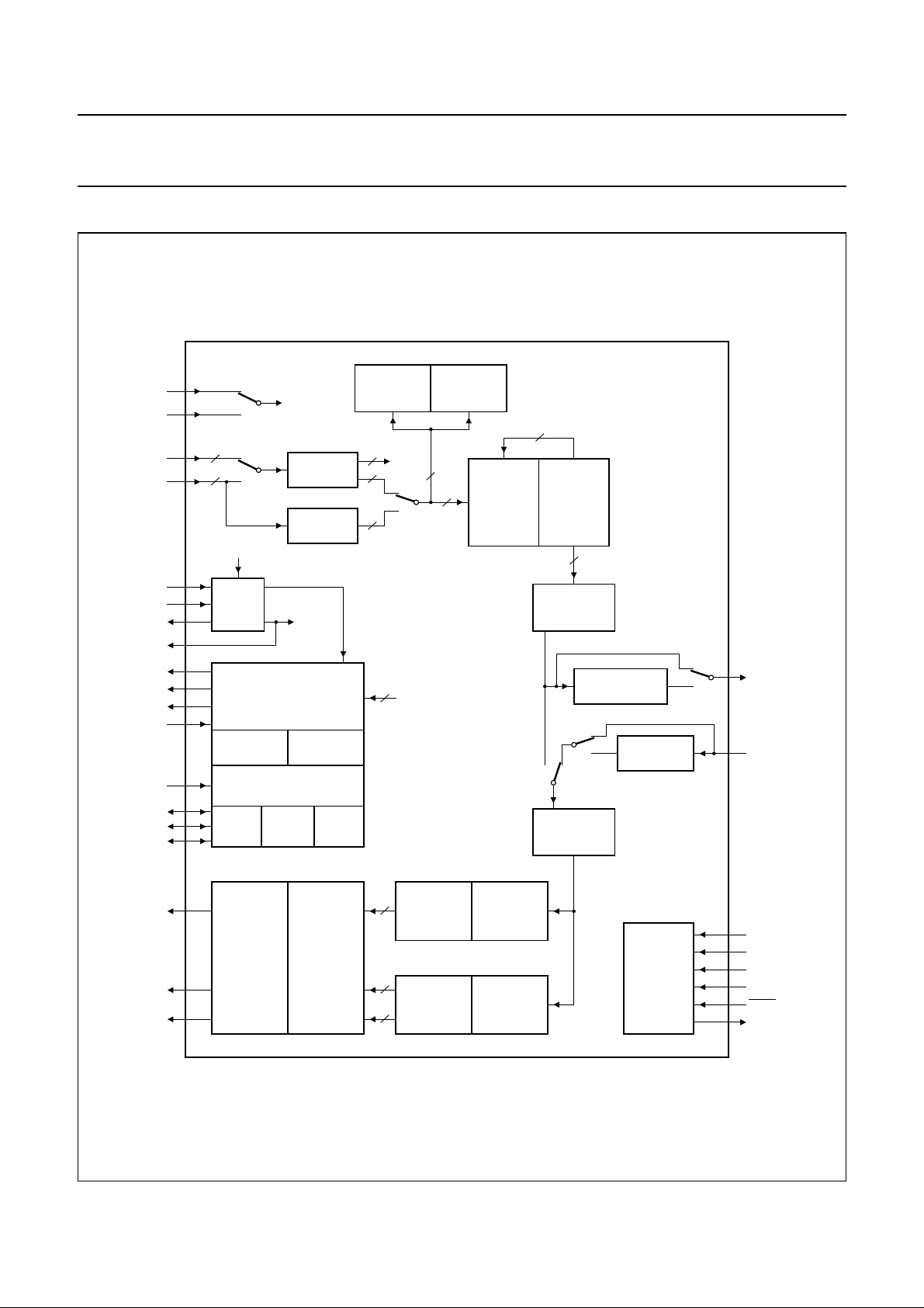
5 BLOCK DIAGRAM
handbook, full pagewidth
]
Y[7:0
8
FAST
SWITCH
H, V
BLACK BAR
DETECTOR
16
REDUCTION
DYNAMIC
NOISE
SOURCE
SELECT
16
LLC1
LLC2
DI17 to DI10
DI27 to DI20
EXT_CLK
OSCI
OSCO
CLK32
HD, VD, ADS
REO, IE, OIE2
RE2, RSTR2
REI, RSTW2
RST
P1.2 to P1.5
SNRST
SNDA,SNCL
SDA, SCL
SOURCE
SELECT
8
8
H
PLL
SYSTEM CONTROLLER
ROM
MICROCONTROLLER
I/O
PORT
SNERT-
BUS
CLK27
MAIN CHANNEL
ITU 656
DECODER 1
SUB CHANNEL
ITU 656
DECODER 2
HREF
CLK32
RAM
2
C-BUS
I
NOISE
ESTIMATOR
2
H, V
16
16
2
SAA4979H
FIELD
MEMORY
3.5 MBIT
16
SAMPLE RATE
CONVERSION
27 to 32 MHz
DOWNSAMPLING
BYPASS
PANORAMIC
ZOOM
UPSAMPLING
SAA4979H
BYPASS
YO7 to YO0
UVO7 to UVO0
YI7 to YI0
UVI7 to UVI0
LUMINANCE CIRCUIT
NON-LINEAR
10
YOUT
UOUT
VOUT
TRIPLE
10-BIT
DAC
POST
PROCESSING
BLANKING
FRAMING
SIDE PANEL
PHASE
FILTER
CHROMINANCE CIRCUIT
10
10
DCTI
Fig.1 Block diagram.
2002 May 28 4
HORIZONTAL
SMART
Y PEAKING
UPSAMPLING
4 : 2 : 2
to
4 : 4 : 4
UV
Y
BCE
BOUNDARY
SCAN
TEST
MHC186
TDI
TCK
TMS
TRST
TDO

Philips Semiconductors Product specification
Sample rate converter with embedded high quality
dynamic noise reduction and expansion port
6 PINNING
SYMBOL PIN TYPE DESCRIPTION
V
DDO1
RSTR2 2 digital output (test input) reset read, source 2
RE2 3 digital output (test input) read enable, source 2
OIE2 4 digital output (test input) output/input enable, source 2
V
SSO1
RSTW2 6 digital input reset write, source 2
DI10 7 digital input ITU 656 input bit 0 (LSB), source 1
DI11 8 digital input ITU 656 input bit 1, source 1
DI12 9 digital input ITU 656 input bit 2, source 1
DI13 10 digital input ITU 656 input bit 3, source 1
DI14 11 digital input ITU 656 input bit 4, source 1
DI15 12 digital input ITU 656 input bit 5, source 1
DI16 13 digital input ITU 656 input bit 6, source 1
DI17 14 digital input ITU 656 input bit 7 (MSB), source 1
V
SSD1
LLC1 16 digital input 27 MHz clock signal, source 1
V
DDD1
V
DDP
DI20 19 digital input ITU 656 input bit 0 (LSB), source 2
DI21 20 digital input ITU 656 input bit 1, source 2
DI22 21 digital input ITU 656 input bit 2, source 2
DI23 22 digital input ITU 656 input bit 3, source 2
DI24 23 digital input ITU 656 input bit 4, source 2
DI25 24 digital input ITU 656 input bit 5, source 2
DI26 25 digital input ITU 656 input bit 6, source 2
DI27 26 digital input ITU 656 input bit 7 (MSB), source 2
V
SSD2
LLC2 28 digital input 27 MHz clock signal, source 2
V
DDD2
TCK 30 digital input test clock
TDI 31 digital input test data input
TMS 32 digital input test mode select
TRST 33 digital input test reset (active LOW)
n.c. 34 to 41 − not connected
TDO 42 digital output test data output
V
DDA1
YOUT 44 analog output Yanalog output
V
SSA1
UOUT 46 analog output −(B − Y) analog output
V
DDA2
1 supply I/O supply voltage 1 (3.3 V)
5 ground I/O ground 1
15 ground digital ground 1
17 supply digital supply voltage 1 (3.3 V)
18 supply protection supply voltage (5 V)
27 ground digital ground 2
29 supply digital supply voltage 2 (3.3 V)
43 supply analog supply voltage 1 (3.3 V)
45 ground analog ground 1
47 supply analog supply voltage 2 (3.3 V)
SAA4979H
2002 May 28 5

Philips Semiconductors Product specification
Sample rate converter with embedded high quality
SAA4979H
dynamic noise reduction and expansion port
SYMBOL PIN TYPE DESCRIPTION
VOUT 48 analog output −(R − Y) analog output
V
SSA2
AGND 50 ground analog ground (without substrate contacts)
BGEXT 51 analog I/O band gap external I/O
V
DDA3
V
SSO2
HD 54 digital output horizontal synchronisation output, display part
VD 55 digital output vertical synchronisation output, display part
V
SSA3
V
DDI
OSCI 58 analog input oscillator input
OSCO 59 analog output oscillator output
CLKEXT 60 digital input external clock input
V
DDD3
CLK32 62 digital output 32 MHz clock output
V
SSD3
V
DDO2
UVI0 65 digital input UV digital input bit 0 (LSB)
UVI1 66 digital input UV digital input bit 1
UVI2 67 digital input UV digital input bit 2
UVI3 68 digital input UV digital input bit 3
UVI4 69 digital input UV digital input bit 4
UVI5 70 digital input UV digital input bit 5
UVI6 71 digital input UV digital input bit 6
UVI7 72 digital input UV digital input bit 7 (MSB)
YI0 73 digital input Y digital input bit 0 (LSB)
YI1 74 digital input Y digital input bit 1
YI2 75 digital input Y digital input bit 2
YI3 76 digital input Y digital input bit 3
YI4 77 digital input Y digital input bit 4
YI5 78 digital input Y digital input bit 5
YI6 79 digital input Y digital input bit 6
YI7 80 digital input Y digital input bit 7 (MSB)
REI 81 digital input read enable input
V
SSO3
IE 83 digital output input enable
REO 84 digital output read enable output
YO7 85 digital output Y digital output bit 7 (MSB)
YO6 86 digital output Y digital output bit 6
YO5 87 digital output Y digital output bit 5
YO4 88 digital output Y digital output bit 4
49 ground analog ground 2
52 supply analog supply voltage 3 (3.3 V)
53 ground I/O ground 2
56 ground analog ground 3
57 supply I/O internal supply voltage (3.3 V)
61 supply digital supply voltage 3 (3.3 V)
63 ground digital ground 3
64 supply I/O supply voltage 2 (3.3 V)
82 ground I/O ground 3
2002 May 28 6

Philips Semiconductors Product specification
Sample rate converter with embedded high quality
dynamic noise reduction and expansion port
SYMBOL PIN TYPE DESCRIPTION
V
DDO3
YO3 90 digital output Y digital output bit 3
YO2 91 digital output Y digital output bit 2
YO1 92 digital output Y digital output bit 1
YO0 93 digital output Y digital output bit 0 (LSB)
V
SSO4
UVO7 95 digital output UV digital output bit 7 (MSB)
UVO6 96 digital output UV digital output bit 6
UVO5 97 digital output UV digital output bit 5
UVO4 98 digital output UV digital output bit 4
V
DDO4
UVO3 100 digital output UV digital output bit 3
UVO2 101 digital output UV digital output bit 2
UVO1 102 digital output UV digital output bit 1
UVO0 103 digital output UV digital output bit 0 (LSB)
V
SSD4
V
DDD4
ADS 106 digital output auxiliary display signal
SNCL 107 digital output SNERT clock
SNDA 108 digital I/O SNERT serial data
V
SSO5
SNRST 110 digital I/O SNERT restart (port 1.0)
SDA 111 digital I/O I
SCL 112 digital I/O I
P1.5 113 digital I/O port 1 data input/output signal 5
P1.4 114 digital I/O port 1 data input/output signal 4
P1.3 115 digital I/O port 1 data input/output signal 3
P1.2 116 digital I/O port 1 data input/output signal 2
V
DDO5
RST 118 digital input microcontroller reset input
n.c. 119 to 127 − not connected
BCE 128 digital input boundary scan compliant enable
89 supply I/O supply voltage 3 (3.3 V)
94 ground I/O ground 4
99 supply I/O supply voltage 4 (3.3 V)
104 ground digital ground 4
105 supply digital supply voltage 4 (3.3 V)
109 ground microcontroller I/O ground
2
C-bus serial data (port 1.7)
2
C-bus clock (port 1.6)
117 supply microcontroller I/O supply voltage (3.3 V)
SAA4979H
2002 May 28 7

Philips Semiconductors Product specification
Sample rate converter with embedded high quality
dynamic noise reduction and expansion port
handbook, full pagewidth
V
DDO1
RSTR2
RE2
OIE2
V
SSO1
RSTW2
DI10
DI11
DI12
DI13
DI14
DI15
DI16
DI17
V
SSD1
LLC1
V
DDD1
V
DDP
DI20
DI21
DI22
DI23
DI24
DI25
DI26
DI27
V
SSD2
LLC2
V
DDD2
TCK
TDI
TMS
BCE
n.c.
n.c.
n.c.
n.c.
n.c.
n.c.
n.c.
n.c.
128
127
126
125
124
123
122
121
120
1
2
3
4
5
6
7
8
9
10
11
12
13
14
15
16
17
18
19
20
21
22
23
24
25
26
27
28
29
30
31
32
n.c.
119
RST
118
DDO5
V
117
P1.2
P1.3
P1.4
P1.5
116
115
114
113
SAA4979H
SCL
112
SDA
111
SSO5
SNRST
V
110
109
SNDA
108
SNCL
107
ADS
106
DDD4VSSD4
V
105
104
UVO0
103
UVO1
102
UVO2
101
UVO3
V
100
DDO4
UVO4
999897
SAA4979H
UVO5
96
UVO6
95
UVO7
V
94
SSO4
93
YO0
92
YO1
91
YO2
90
YO3
V
89
DDO3
88
YO4
87
YO5
86
YO6
85
YO7
84
REO
83
IE
V
82
SSO3
81
REI
80
YI7
79
YI6
78
YI5
77
YI4
76
YI3
75
YI2
74
YI1
73
YI0
72
UVI7
71
UVI6
70
UVI5
69
UVI4
68
UVI3
67
UVI2
66
UVI1
65
UVI0
33343536373839404142434445464748495051525354555657585960616263
n.c.
n.c.
n.c.
n.c.
n.c.
n.c.
n.c.
n.c.
TRST
TDO
DDA1
V
YOUT
V
SSA1
UOUT
DDA2
V
Fig.2 Pin configuration.
2002 May 28 8
VOUT
V
SSA2
AGND
DDA3VSSO2
V
BGEXT
HD
VD
SSA3
V
V
DDI
OSCI
OSCO
CLKEXT
DDD3
V
SSD3
CLK32
V
64
DDO2
V
MHC200

Philips Semiconductors Product specification
Sample rate converter with embedded high quality
dynamic noise reduction and expansion port
7 FUNCTIONAL DESCRIPTION
7.1 Digital processing at 1fH level
7.1.1 ITU 656
The SAA4979H provides 2 digital video input channels,
which comply to the ITU 656 standard.
720 active video pixels per line are processed at a
line-locked clock of 27 MHz, which has to be provided by
the signal source. Luminance and chrominance
information have to be multiplexed in the following order:
CB1,Y1,CR1,Y2, ... Timing reference codes must be
inserted at the beginning and end of each video line
(see Table 1):
• A ‘Start of Active Video’ (SAV) code before the first
active video sample (see Table 2)
• A ‘End of Active Video’ (EAV) code after the last active
video sample (see Table 2).
Table 1 ITU data format
DECODER
Theincomingactive video data must belimitedto1 to 254,
since the data words 00H and FFH are used for
identification of the timing reference headers.
The digital signal input levels should comply to the
CCIR-601 standard (see Fig.3). The data stream is
decoded into the internal 4 :2:2 YUV format at a
13.5 MHz clock rate. If required the sign of the UV signals
canbe inverted for bothchannels (control inputs: uv_sign1
and uv_sign2).
The signal source of the main channel can be selected
from both inputs by the internal microcontroller (control
input: Select_data_input1).
SAA4979H
BLANKING
PERIOD
... 80 10 FF 00 00 SAV C
Table 2 SAV/EAV format
BIT 7
1 field bit
1st field: F = 0;
2nd field: F = 1
TIMING
REFERENCE
CODE (HEX)
BIT 6
(F)
TIMING
720 PIXELS YUV 4 :2:2 DATA
0Y0CR0Y1CB2 Y2 ... CR718 Y719 FF 00 00 EAV 80 10 ...
B
BIT 5
(V)
vertical blanking bit
VBI: V = 1;
active video: V = 0
H = 0 in SAV format;
H = 1 in EAV format
BIT 4
(H)
REFERENCE
CODE (HEX)
BIT 3
(P3)
reserved; evaluation not
recommended (protection bits
according to ITU 656)
BIT 2
(P2)
BLANKING
PERIOD
BIT 1
(P1)
BIT 0
(P0)
2002 May 28 9

Philips Semiconductors Product specification
Sample rate converter with embedded high quality
dynamic noise reduction and expansion port
+
handbook, full pagewidth
255
+
235
+
128
+
white
LUMINANCE 100%
16
0
black
a. Y output range. b. U output range (CB). c. V output range (CR).
+
255
+
240
+
212
+
128
+
44
+
16
0
blue 100%
blue 75%
colourless
U-COMPONENT
yellow 75%
yellow 100%
+
255
+
240
+
212
+
128
+
44
+
16
0
SAA4979H
red 100%
red 75%
colourless
V-COMPONENT
cyan 75%
cyan 100%
MHC201
It should be noted that the input levels are limited to 1 to 254 in accordance with ITU 601/656 standard.
Fig.3 Digital video input levels.
7.1.2 DOUBLE WINDOW AND PICTURE-IN-PICTURE
PROCESSING
Data from the sub channel can be inserted into the data
stream of the main channel by means of afast switch.The
two channels can be used together with one or two
external field memoriesto implement, for example, double
window or PIP processing. Both field based and frame
based PIP processing is supported. The synchronization
of the sub channel to the main channel is achieved by
providingsynchronized read signals(RE2and RSTR2) for
the external field memories, whereas the write signals
needto be providedtogether with the incomingdata by the
external signal source.
A multi-PIP mode is also supported by freezingthe data in
the internal field memory within certain areas via the
programmable internal control signal IE
.
int
7.1.3 BLACK BAR DETECTOR
Black bar detection searches for the last black line in the
upper part of the screen and for the first black line in the
lower part of the screen. The detection is done within a
programmable window (control inputs: bbd_hstart,
bbd_hstop, bbd_vstart and bbd_vstop). To avoid
disturbances of LOGOs in the video, the window can be
shifted to the horizontal centre of the lines. A video line is
considered to be black if the luminance values of that line
within the detection window are not greater than a certain
slice level (control input: bbd_slice_level) for more than a
specific number of pixels (control input: bbd_event_value).
The numbers of the first and the last active video line can
be read out by the microcontroller (control outputs:
bbd_1st_videoline and bbd_last_videoline).
2002 May 28 10

Philips Semiconductors Product specification
Sample rate converter with embedded high quality
dynamic noise reduction and expansion port
7.1.4 DYNAMIC NOISE REDUCTION
The main function of the noise reduction is shownin Fig.4.
It is divided into two signal paths for chrominance and
luminance. In principal two operating modes can be used,
the fixed and the adaptive mode. In both modes the
applied frequency range, in which the noise reduction
takes place, can be reduced or not reduced (control input:
unfiltered).
The noise reduction operates field recursive with an
averaging ratio (K factor) between fresh (new) and over
previousfieldsaveraged(old)luminanceandchrominance
values. Noise reduction can be activated by forcing the
NREN control bit to HIGH. If NREN is LOW the noise
reduction block is bridged via a data multiplexer.
Inthe fixed mode,thenoise reduction producesaconstant
weighted input averaging. Because of smearing effects
this mode should not be used for normal operation except
for K = 1. The fixed mode can be activated separately for
chrominance (control input: chromafix) and luminance
(control input: lumafix).
It should be noted that recursion is done over fields, and
that pixel positions between the new and old fields always
have a vertical offset of one line. So averaging is not only
done in the dimension of time but also in the vertical
direction.Therefore averaging verticallyon, for example, a
vertical black to white edge would produce a grey result.
The averaging in chrominance can optionally be slaved to
the luminance averaging (control input: Klumatochroma),
in that case chrominance differences are not taken into
account for the K factor setting of the chrominance signal
path.
The noise reduction scheme also decreases the
cross-colour patterns effectively if the adaptive noise
reductionfor the averagingin chrominance isslaved to the
luminance averaging (control input: Klumatochroma). The
cross-colour pattern does not produce an increase of the
measured luminance difference, therefore this pattern will
be averaged over many fields.
SAA4979H
In the adaptive mode, the averaging ratio is based on the
absolute differences of the inputs of luminance and
chrominancerespectively. If the absolutedifferenceis low,
only a small part of the fresh data will be added. In cases
of high difference, much of the fresh data will be taken.
This occurs either in situations of movement or where a
significant vertical contrast is seen. The relationship
between the amount of movement andthe K factor values
is defined in a look-up table where the steps can be
programmed (control input: Kstep).
2002 May 28 11

Philips Semiconductors Product specification
Sample rate converter with embedded high quality
dynamic noise reduction and expansion port
handbook, full pagewidth
control input:
unfiltered
data input
UV7 to UV0
8
new U/V
delta U/V
LOW-PASS
FILTER 1
LF delta U/V
Dfielddelay
UV7 to UV0
8
old U/V
control input:
unfiltered
data input
Y7 to Y0
8
new Y
delta Y
LOW-PASS
FILTER 1
SAA4979H
Dfielddelay
Y7 to Y0
8
old Y
LF delta Y
control input:
Cadapt_gain
ABS/LIMITER
UV
AVERAGE
LOW-PASS
FILTER 2
LUT
Kchroma
Kchromafix
Kluma
control input:
noiseshape
control input:
chromafix and
Klumatochroma
NOISE SHAPE
Dtomemory
UV7 to UV0
HF delta U/V
processed UV
8
control input:
Yadapt_gain
ABS/LIMITER
LOW-PASS
FILTER 2
LUT
Klumafix
Kluma
control input:
noiseshape
MHC202
HF delta Y
control input:
lumafix
processed Y
NOISE SHAPE
8
Dtomemory
Y7 to Y0
Fig.4 Schematic diagram of noise reduction.
2002 May 28 12

Philips Semiconductors Product specification
Sample rate converter with embedded high quality
dynamic noise reduction and expansion port
7.1.4.1 Band-splitting
The frequencies of the difference signals of luminance
(delta Y) and chrominance (delta U/V) can be split
optionally into an upper band (HF) and a lower band (LF)
with a low-pass filter in both signal paths. The lower
frequency band signals (LF delta Y and LF delta U/V) are
used as input for the noise reduction function.
The lower frequency band of the difference signals can
also be used for the motion detection. If, for example, only
the lower frequency band contains information, the
specific picture content does not move or is moving slowly.
Optionallyit is possibleto bridge theband-splitting (control
input: unfiltered = 1).
7.1.4.2 Motion detection
The same signals (the noise reduction is applied to) are
also used to detect the amount of motion in the difference
signals. Therefore, the absolute values of the difference
signals are generated and limited to a maximum value.
Theabsolute values of thedifferencesignal of U and V are
then averaged. The signals are low-pass filtered for
smoothingthesesignals.Thefiltered signals are amplified,
depending on the setting of the control inputs:
Yadapt_gain and Cadapt_gain respectively.
The amplified signals, which correlate to the amount of
movement in the chrominance or luminance signal path,
are transferred into 1 out of 9 possible K factor values via
look-up tables. The look-up tables consist of 9 intervals,
each related to one K factor. The boundaries between the
9 intervals are defined by 8 programmable steps (control
inputs:Kstep0 to Kstep7). The step values arevalidfor the
look-uptablesforboth the chrominance and theluminance
path. For example, signal values between Kstep2 and
Kstep3 result in a K factor of K =3/8.
7.1.4.3 K factor
The amount of noise reduction (field averaging) is
described my means of the K factor. When K = 1 no
averaging is applied and the new field information is used.
When K = 0 no averaging is applied and thus only the old
field information is used like in a still picture mode. All
values inbetween mean that a weighted averaging is
applied. It is possible to use fixed K factor values if the
control inputs lumafix or chromafix are set to logic 1. The
possible fixed K factor values of the control inputs
Klumafix and Kchromafix are given in Table 6.
7.1.4.4 Noise shape
Possible shadow picture information in the chrominance
and luminance path, resulting from a low K factor value,
will be eliminated if the noise shaping is activated. The
noise shaping function can be switched off via the
microcontroller (control input: noiseshape).
7.1.5 NOISE ESTIMATOR
The noise level of the luminance signal can be measured
within a programmable window (control inputs: ne_hstart,
ne_hstop, ne_vstart and ne_vstop). The correlation in flat
areas is used to estimate the noise in the video signal.
A large number of estimates of the noise is calculated for
every video field. Such an estimate is obtained by
summing absolute differences between current pixel
values and delayed pixel values within blocks of 4 pixels.
Within the lower part of the total range of possible
estimates15 intervals are defined. Eachintervalis defined
by a lower boundary and an upper boundary. The lower
boundary is equal to the number of the interval, whereas
the upper boundary has a fixed relationship to the lower
boundary (control input: gain_upbnd).
The lower boundary is increased or decreased by 1 in
each field until an interval is found which contains at least
a predefined number of estimates, and is at thesame time
lowestin the range. Thevalueofthe lower boundary ofthis
interval determines the current noise figure output. The
predefined number of estimates can be set via the
microcontroller (control input: wanted_value), and good
results were obtained with a value which is approximately
0.27% of the total number of blocks.
For video fields with a lot of noise the number of small
differences is very low, that means the number of noise
estimates in the lower intervals is close to 0. Contrary to
this, for clean sequences this number is very high. This
means that for clean sequences the noise estimate figure
will be close to 0, and for sequences with a lot of noise the
noise estimate figure (control output: nest) will reach 15.
To improve the performance of the noise estimator,
severalfunctionsareimplementedwhich can be controlled
by the microcontroller. To increase the sensitivity of the
noise measurement a prefilter with different gain settings
is available (control input: Ypscale). Since the video
content, e.g. sequences with a lot of high frequencies,can
influence the noise estimate figure, a detail-counter is
built-in.
SAA4979H
2002 May 28 13

Philips Semiconductors Product specification
Sample rate converter with embedded high quality
dynamic noise reduction and expansion port
The detail-counter calculates the number of absolute
differences between current and previous pixels within a
programmable interval defined by the control inputs
lb_detail and upb_detail. The result of the 16-bit
detail-counter (control outputs: detail_cnt_h and
detail_cnt_l) can be used to increase or decrease the
result of the noise estimation figure (control input:
compensate).
In order to reduce the effect of clipping, only the blocks
where the sum of the luminance value is within a
predefined range are taken into account. The control
signal clip_offs can be used to increase or decrease this
range. A grey-counter gives information whether enough
pixels with values in the grey range are present in a video
field (control output: grey_cnt). When this number is lower
than a predefined threshold, e.g. for complete fields
towards black or white, all blocks are taken into account.
7.2 Embedded DRAM
7.2.1 3.5-MBIT FIELD MEMORY
Thebasic functionality ofthefield memory, whichisshown
in Fig.5, is similar to the SAA4956TJ. The memory size is
extended to 3538944 bits. The data path is 16-bit wide
(8-bitchrominanceand 8-bit luminance). The fieldmemory
is capable of storing, for example, up to 307 video lines of
720 pixels in a 4:2:2 format. After writing or reading
18 words of 16-bit width, a data transfer is performed from
the serial to parallel data registers (writing) or from the
parallel to the serial registers (reading). The field memory
has one write interface (controller and registers) to store
1fHdata and two read interfaces, one to read field delayed
1fH data for the noise reduction function and the other to
read 2fHdata for the following data processing. Since two
asynchronous clock domains are involved (SWCKint as
1fHclock and SRCKint as 2fHclock) the read and write
access to the memory array is controlled asynchronously
by the memory arbitration logic triggered via request and
acknowledge pulses.
The write operation starts with a reset write (RSTWint)
address pointer operation during the write enable (WEint)
LOW phase. The RSTWint LOW-to-HIGH transition,
referred to the rising edge of the write clock SWCKint,
must be at least 18 clock cycles ahead of the first written
data (WEint HIGH) and 18 clock cycles after the last
written data. The reset write transfers data temporarily
stored in theserial write registers to the memory arrayand
resets the write counter to the lowest address. Write
enable (WEint) is used to enable or disable a data write
operation. The WEintsignal controls the data inputs
D0 to D15.
In addition, the internal write address pointer is
incremented if WEint is HIGH at the positive transition of
the SWCKint write clock. The data is latched if WEint was
HIGH at the previous positive transition of SWCKint. Input
enable (IEint) LOW can also suppress the storage of the
datainto the memory arraybutdoes not influencethewrite
pointerincrement. It isused to freeze partsof the fielddata
e.g for PIP processing.
The read operation starts with a reset (RSTRint) of the
read address pointer during the read enable (REint) LOW
phase. The RSTRint LOW-to-HIGH transition, referred to
the rising edgeof the read clock SRCKint, must beat least
18 clock cycles ahead of the first read data (REint HIGH)
and18 clock cycles afterthe last read data.The reset read
resetstheread counter to the lowestaddressandrequests
a read operation of the data of the lowest address to the
serial read register. Read enable (REint) is used to enable
or disable the read operation. The REint controls the data
outputs Q0 to Q15. REint HIGH increments the read
counter.
In parallel to the write operation a read2 operation is done
using the same control signals as the write operation:
SWCKint, WEint and RSTWint. It reads the old data of the
previous field. The data Qold is needed as data input
(Dfielddelay) for the noise reduction.
When the WEint signal is HIGH it indicates that active
video (valid 1fH data) is to be stored. The start of WEint
HIGH is triggered by the H and V status bits of the ITU
data stream. The start of WEint HIGH can be delayed by
the control signals weint_hstart (number of clock delays)
andweint_vstart (number ofvideolines delay). Thestopof
WEint HIGH is controlled by weint_hstop and weint_vstop.
When the IEint signal is HIGH it indicatesthat active video
(valid 1fH data) is also to be stored. The video data is not
stored and earlier written data is maintained (frozen) if
WEint is HIGH and IEint is LOW.The startof IEintHIGH is
triggeredby the H and V status bitsofthe ITU data stream.
The start of IEint HIGH can be delayed by the control
signals ieint_hstart (number of clock delays) and
ieint_vstart (number ofvideo lines delay). The stop of IEint
HIGH is controlled by ieint_hstop and ieint_vstop.
RSTWint is triggered by the V status bit of the ITU data
stream.
RSTRintis identical to the VD output signal.
REint is provided by the following sample rate conversion
to gather 2fH data if it is needed.
SAA4979H
2002 May 28 14

Philips Semiconductors Product specification
Sample rate converter with embedded high quality
dynamic noise reduction and expansion port
handbook, full pagewidth
D15 to D0 and IEint WEint RSTWint SWCKint
17
SERIAL WRITE REGISTER
18-WORD (×17)
18 × (16 + 1)
PARALLEL WRITE REGISTER
18-WORD (×17)
18 × (16 + 1)
MEMORY ARRAY
221184-WORD (×16)
address
and
control
SAA4979H
SERIAL WRITE CONTROLLER
write control
(requests
reset/next)
WRITE ADDRESS
COUNTER
READ2 ADDRESS
COUNTER
MEMORY
ARBITRATION
LOGIC
18 × 16
PARALLEL READ2 REGISTER
18-WORD (×16)
18 × 16
SERIAL READ2 REGISTER
18-WORD (×16)
read2
acknowledge
SERIAL READ2 CONTROLLER
WEint RSTWint SWCKint Qold15 to Qold0 Q15 to Q0
read2
control
(requests
reset/next)
PARALLEL READ REGISTER
SERIAL READ REGISTER
18 × 16
18-WORD (×16)
18 × 16
18-WORD (×16)
SERIAL READ CONTROLLER
1616
REint RSTRint SRCKint
read
control
(requests
reset/next)
READ ADDRESS
COUNTER
read
acknowledge
MHC190
Fig.5 Schematic diagram of 3.5-Mbit field memory.
2002 May 28 15

Philips Semiconductors Product specification
Sample rate converter with embedded high quality
dynamic noise reduction and expansion port
7.3 Digital processing at 2fH level
7.3.1 S
The sample rate conversion block is used to obtain
848 active pixels per line out of the original 720 pixels
according to the relation of the two sampling frequencies
(32 MHz and 27 MHz). The interpolation for phase
positions between the original samples is achieved with a
variable phase delay filter with 10 taps for luminance
signals and 6 taps for chrominance signals.
The conversion toa higher samplefrequency of 32 MHz is
done to improve the motion estimation performance in
combination with external feature ICs, which can process
up to 848 pixels per line at a 32 MHz clock. Bypassing this
function keeps the original 720 pixels per line (control
input: bypass_FSRC).
7.3.2 E
For a further extension of the system an expansion port is
available, which is applicable for eithera 4:2:2format or
a reduced 4:1:1 format for data input and output at a
32 MHz line-locked clock; see Table 3. However, the
internal data is processed in a 8-bit wide 4 :2:2format.
To generate the 4:1:1 format at the output the U and V
samples from the 4 : 2 : 2 data stream are filtered by a
low-pass filter, before being subsampled with a factor of 2
and formatted to 4:1:1 format. Bypassing this function
keeps the data in the 4:2:2 format.
AMPLE RATE CONVERSION
XPANSION PORT
An internal bandwidth detector is implemented to detect
whetherthe colour differencesignals provide eitherthe full
4:2:2bandwidth or a reduced 4 : 1 : 1 bandwidth.
Therefore absolute differences between original data and
downsampled data are calculated and can be read out by
the microcontroller (control output: UV_bw_detect). Low
absolute differences indicate that the original data does
not contain the full 4:2:2bandwidth. This information
canbe used toswitch the upsampleand downsample filter
on or off (control inputs: bypass_upsampling and
bypass_downsampling). Bandwidth detection is done
within a programmable window (control inputs: bw_hstart,
bw_hstop and bw_vstart, bw_vstop).
Inthe event ofa 4 : 1 : 1 format atthe input anupconverter
to 4:2:2 is applied with a linear interpolation filter for
creation of the extra samples. These are combined with
the original samples from the 4 : 1 : 1 stream.
The first phase of the YUV data stream is available on the
output bus twoclock cycles afterthe rising edge of theREI
input signal. The start position, when the first phase of the
YUV data stream arrives on the input bus, can be set via
the control register exp_hstart.
The luminance output signal is in 8-bit straight binary
format, whereas the chrominance output signals are in
twos complement format. The input data at the expansion
slot is expected in the same format. U and V input signals
are inverted if the corresponding control bit mid_uv_inv is
set.
SAA4979H
Table 3 YUV formats
OUTPUT PIN 4:1:1 FORMAT 4:2:2 FORMAT INPUT PIN
YO7 Y07 Y17 Y27 Y37 Y07 Y17 YI7
YO6 Y06 Y16 Y26 Y36 Y06 Y16 YI6
YO5 Y05 Y15 Y25 Y35 Y05 Y15 YI5
YO4 Y04 Y14 Y24 Y34 Y04 Y14 YI4
YO3 Y03 Y13 Y23 Y33 Y03 Y13 YI3
YO2 Y02 Y12 Y22 Y32 Y02 Y12 YI2
YO1 Y01 Y11 Y21 Y31 Y01 Y11 YI1
YO0 Y00 Y10 Y20 Y30 Y00 Y10 YI0
UVO7 U07 U05 U03 U01 U07 V07 UVI7
UVO6 U06 U04 U02 U00 U06 V06 UVI6
UVO5 V07 V05 V03 V01 U05 V05 UVI5
UVO4 V06 V04 V02 V00 U04 V04 UVI4
UVO3 −−−−U03 V03 UVI3
UVO2 −−−−U02 V02 UVI2
UVO1 −−−−U01 V01 UVI1
UVO0 −−−−U00 V00 UVI0
2002 May 28 16

Philips Semiconductors Product specification
Sample rate converter with embedded high quality
dynamic noise reduction and expansion port
7.3.3 PANORAMIC ZOOM
Thepanoramic zoom blockcontains a secondsample rate
converter, which performs the following tasks:
• Linear horizontal sample rate conversion in both zoom
and compress direction, with a sample rate conversion
factor between 0 and 2, meaning infinite zoom up to a
compression with a factor of 2
• Dynamic sample rate conversion e.g. for panorama
mode display of 4 : 3 material on a 16 : 9 screen.
Forlinear horizontal zoomor compression thesample rate
conversion factor is static during a video line (control
input: c0). Positive values of c0 are suitable for
compression, negative values result in expansion.
In panorama mode the video lines are geometrically
expanded towards the sides. The sample rate conversion
factoris modulated alongthe video line.A parabolic shape
of the sample rate conversion factor can be obtained with
the parameter c2, which controls the second order
variation of the sample rate. Negative values of c2 are
suitable for panorama mode, positive values result in the
inverse mode (amaronap mode).
The panoramic zoom block also provides a dynamically
controlled delay with an accuracy up to1⁄64 of a pixel and
a range of −0.5 to +0.5 lines (control input: hshift).
Sufficient accuracy in interpolation for phase positions
between the original samples is achieved with a variable
phase delay filter with 10 taps for luminance signals and
6 taps for chrominance signals.
7.3.4 DIGITAL COLOUR TRANSIENT IMPROVEMENT
The Digital Colour Transient Improvement (DCTI) is
intended for U and V signals originating from a 4:1:1
source. Horizontal transients are detected and enhanced
without overshoots by differentiating, make absolute and
again differentiating the U and V signals separately. This
results in a 4:4:4 UandV bandwidth. To prevent
third-harmonic distortion, which is typical for this
processing, a so called over the hill protection prevents
peak signals becoming distorted.
It is possible to control the following settings via the
microcontroller: gain width (see Fig.10), threshold (i.e.
immunity against noise), selection of simple or improved
first differentiating filter (see Fig.9), limit for pixel shift
range (see Fig.11), common or separate processing of
U and V signals, hill protection mode (i.e. no
discolourations in narrow colour gaps), low-pass filtering
for U and V signals (see Fig.12) and a so called super hill
mode, which avoids discolourations in transients within a
colour component.
7.3.5 HORIZONTAL SMART Y PEAKING
A linear peaking is applied, which amplifies the luminance
signal in the middle and the upper ranges of the
bandwidth.
The filtering is an addition of:
• The original signal
• The original signal high-passed with maximum gain at a
frequency of1⁄2fs (sample frequency fs= 32 MHz)
• Theoriginal signal band-passedwith a centre frequency
of1⁄4f
s
• Theoriginal signal band-passedwith a centre frequency
of 4.76 MHz.
The band-passed and high-passed signals are weighted
with the factors 0,1⁄16,2⁄16,3⁄16,4⁄16,5⁄16,6⁄16 and8⁄16,
resulting in a maximum gain difference of 2 dB per step at
the centre frequencies.
Coring is added to avoid amplification of low amplitudes in
the high-pass and band-pass filtered signals, which are
considered to be noise. The coring threshold can be
programmed as 0 (off), ±4, ±8, ±12 to ±60 LSB with
respect to the (signed) 10-bit signal.
In addition the peaking gain can be reduced dependingon
the signal amplitude, programming range 0 (no
attenuation),1⁄4,2⁄4and4⁄4. It is also possible to make
largerundershootsthanovershoots,programming range 0
(no attenuation of undershoots),1⁄4,2⁄4and4⁄4.
A steepness detector is built-in, which provides
informationfor dynamic controlof the peaking.For that the
maximum absolute value of the band-pass filtered signal
withina video fieldis calculated andcan be read outby the
microcontroller (control output: steepness_max).
7.3.6 NON-LINEAR PHASE FILTER
The non-linear phase filter adjusts possible group delay
differences in the Y, U and V output channels. The filter
coefficients are: [−λ × (1 −µ); 1 + λ; −λ×µ] where
λ determinesthestrength of the filterandµ determinesthe
asymmetry. The effect of the asymmetry is a decrease in
the delay for higher frequencies with µ≤0.5. Control
settings are provided for λ =0,1⁄8,2⁄8,3⁄8and µ =0,1⁄4,1⁄2.
SAA4979H
2002 May 28 17

Philips Semiconductors Product specification
Sample rate converter with embedded high quality
dynamic noise reduction and expansion port
7.3.7 POST PROCESSING
Blanking is done just before the digital-to-analog
conversion by switching Yto afixed black value and UVto
a colourless value. The blanking window is defined by the
control inputs: bln_hstart, bln_hstop, bln_vstart and
bln_vstop.
Side panels are generated by switching the Y, U and V to
defined values within a horizontal window (control inputs:
sidepanel_hstart and sidepanel_hstop); the 8 MSBs of Y
and the 4 MSBs of U and V are programmable (control
inputs: sidepanel_y, sidepanel_u and sidepanel_v).
Framing e.g. for picture-in-picture mode, can be achieved
by another programmable window (control inputs:
PIP_frame_hstart, PIP_frame_hstop, PIP_frame_vstart
and PIP_frame_vstop). The vertical and horizontal frame
width can be programmed from 1 up to 15 pixels (control
inputs:PIP_frame_heigth and PIP_frame_width). Framing
uses the same colour and luminance values as the side
panels.
The range of the Y output signal can be chosen between
9 and 10 bits (control input: output_range). In the event of
9 bitsfor the nominal signalthere is room leftfor under and
overshoot, adding up to a total of 10 bits. In the event of
selecting all 10 bits of the luminance digital-to-analog
converter for the nominal signal any under or overshoot
will be clipped (see Fig.6).
The Y samples can be shifted onto 16 positions with
respect to the UV samples (control input: y_delay). The
zero delay setting is suitable for the nominal case of
aligned input data. The other settings provide eight
samples with lessdelay to sevensamples with more delay
in Y.
7.4 Triple 10-bit digital-to-analog conversion
Three identical 10-bit converters are used to map the
4:4:4 YUV data to analog levels with a 32 MHz data
rate. The polarity of the colour difference signals U and V
is switchable by the control bit uv_inv_out. The output
ranges are illustrated in Figs 6 and 7 respectively.
SAA4979H
handbook, full pagewidth
(255) 1023
(235) 940
(16) 64
(0) 0
white
black
1.0 V (p-p)
VOY + 1.095 V
VOY + 1.0 V
V
OY
VOY − 0.073 V
1023
(255) 766
(235) 727
(16) 288
(0) 256
white
1.0 V (p-p)
black
0
a. Output range = 1. b. Output range = 0.
Fig.6 Luminance output levels.
VOY + 1.674 V
VOY + 1.0 V
V
OY
VOY − 0.656 V
MHC191
2002 May 28 18

Philips Semiconductors Product specification
Sample rate converter with embedded high quality
dynamic noise reduction and expansion port
handbook, full pagewidth
(255) 1023
(212) 848
(128) 512
(44) 176
(0) 0
blue 75%
colourless
1.33 V (p-p) 1.05 V (p-p)
yellow 75%
VOU + 1.012 V
VOU + 0.665 V
V
OU
VOU − 0.665 V
VOU − 1.012 V
(255) 1023
(212) 848
(128) 512
(44) 176
(0) 0
red 75%
colourless
cyan 75%
SAA4979H
VOV + 0.8 V
VOV + 0.575 V
V
OV
VOV − 0.575 V
VOV − 0.8 V
MHC192
a. U output level. b. V output level.
Fig.7 Chrominance output levels.
7.5 Microcontroller
The SAA4979H contains an embedded 80C51
microcontrollercoreincluding512-byteRAMand32-Kbyte
ROM. The microcontroller runs on a 16 MHz clock,
generated by dividingthe 32 MHz display clock by a factor
of 2.
7.5.1 HOST INTERFACE
For controlling internal registers a host interface,
consisting of a parallel address and data bus, is built-in.
Theinterface can beaddressed as internalAUXRAM via a
MOVX type of instruction. The complete range of internal
control registers and the corresponding host addresses
are described in Section 8.1. User access to these control
registers via the I2C-bus can be implemented in the
embedded software.
2
7.5.2 I
C-BUS INTERFACE
The I2C-bus interface in the SAA4979H is used in a slave
receive and transmit mode for communication with a
central system microcontroller. The standardized bus
frequencies of both 100 kHz and 400 kHz can be
accommodated.
2
The I
C-bus slave address of the SAA4979H is
0110100 R/W. During slave transmit mode the SCL LOW
period may be extended by pulling SCL to LOW (in
accordance with the I2C-bus specification).
Detailed information about the software dependent
I2C-bus subaddresses of the control registers and a
detailed description of the transmission protocol can be
found in Application Note
the SAA4979H”
.
“I2C-bus register specification of
7.5.3 SNERT-BUS INTERFACE
A SNERT interface is built-in, which operates in a master
receive and transmit mode for communication with
peripheral circuits such as SAA4991WP or SAA4992H.
The SNERT interface replaces the standard UART
interface. Contrary to the 80C51 UART interface there are
additional special function registers (see Table 10) and
there is no byte separation time between address and
data.
2002 May 28 19

Philips Semiconductors Product specification
Sample rate converter with embedded high quality
dynamic noise reduction and expansion port
TheSNERT interface transformsthe parallel datafrom the
microcontrollerinto1 or 2 Mbaud SNERT data, switchable
via microcontroller. The SNERT-bus consists of three
signals: SNCL used as serial clock signal, generated by
theSNERT interface; SNDA used asbidirectionaldata line
and SNRST used as reset signal, generated by the
microcontroller at port pin P1.0 to indicate the start of a
transmission.
The read or write operation must be set by the
microcontroller. When writing to the bus, 2 bytes are
loaded by the microcontroller: one for the address, the
other for the data. When reading from the bus, one byte is
loaded by the microcontroller for theaddress, the received
byte is the data from the addressed SNERT location.
7.5.4 I/O PORTS
A parallel 8-bit I/O port (P1) is available, where P1.0 is
used as SNERT reset signal (SNRST), P1.2 to P1.5 can
be used for application specific control signals, and P1.6
and P1.7 are used as I2C-bus signals (SCL and SDA).
7.5.5 WATCHDOG TIMER
The system controller is connected to the microcontroller
via the host interface.
7.6.1 READ ENABLE OUTPUT
The Read Enable Output (REO) signal is intended for
control of an external feature IC. It is a composite signal
consistingofahorizontal and a vertical part. The horizontal
and vertical positions are programmable (control inputs:
reo_hstart, reo_hstop, reo_vstart and reo_vstop).
7.6.2 READ ENABLE INPUT
The Read EnableInput (REI) signalis used in applications
with external feature ICs connected to the expansion port.
It has to be provided by the external circuit (see
Section 7.3.2).
7.6.3 INPUT ENABLE
The Input Enable (IE) signal is intended for control of field
memories in applications together with an external feature
IC connected to the expansion port. It can be directly set
or reset via the microcontroller.
SAA4979H
The microcontroller contains an internal Watchdog timer,
which can be activated by setting the corresponding
special function register PCON.4. Only a synchronous
reset will clear this bit. To prevent a system reset the
Watchdog timer must be reloaded within a specified time.
The Watchdog timer contains an 11-bit prescaler and is
therefore incremented every 0.768 ms (16 MHz clock).
The time interval between the timers reloading and the
occurrence of a reset depends onthe reloaded 8-bit value.
7.5.6 RESET
A reset is accomplished by holding the RST pin HIGH for
at least 0.75 µs while the display clock is running and the
supply voltage is stabilized.
7.6 System controller
The system controller provides all necessary internal read
and write signals for controlling the embedded field
memory. The required control signals (REO and IE) for
applications with motion compensation circuits and the
drive signals (HD and VD) for the horizontal and vertical
deflection power stages are also generated.
The system controller also supports double window or
picture-in-picture processing in combination with an
external field memory by providing the required memory
control signals (RE2, RSTW2 and OIE2).
7.6.4 HORIZONTAL DEFLECTION
The Horizontal Deflection (HD) signal is for driving a
deflection circuit; start and stop values of the horizontal
positionare programmable in a resolutionof4 clock cycles
(control inputs: hd_start and hd_stop).
7.6.5 VERTICAL DEFLECTION
The Vertical Deflection (VD) signal is for driving a
deflectioncircuit. This signalhas a cycle timeof 10 ms and
the start and stop values of the vertical position are
programmable in steps of 16 µs (control inputs: vd_start
and vd_stop).
7.6.6 AUXILIARY DISPLAY SIGNAL
The Auxiliary Display Signal (ADS) is for general
purposes; the horizontal and vertical positions are
programmable (control inputs: ads_hstart, ads_hstop,
ads_vstart and ads_vstop).
7.6.7 READ ENABLE 2
The Read Enable 2 (RE2) signal is intended for control of
an external field memory at input channel 2 in
picture-in-picture applications. It is a composite signal
consistingofahorizontal and a vertical part. The horizontal
and vertical positions are programmable (control inputs:
re2_hstart, re2_hstop, re2_vstart and re2_vstop).
2002 May 28 20

Philips Semiconductors Product specification
Sample rate converter with embedded high quality
dynamic noise reduction and expansion port
7.6.8 OUTPUT/INPUT ENABLE 2
The Output/Input Enable 2 (OIE2) signal is intended for
control of one or two external field memories at input
channel 2 in picture-in-picture applications. It can be
directly set or reset via the microcontroller.
7.6.9 RESET READ 2
The Reset Read 2 (RSTR2) signal is intended for control
of the read access of an external field memory at input
channel 2 in picture-in-picture applications. It is derived
from the internal vertical reference signal of the main
channel.
7.6.10 RESET WRITE 2
The Reset Write 2 (RSTW2) input is used in
picture-in-picture applications with an external field
memory at input channel 2, and has to be provided by an
external circuit which controls the field memory write
access.
7.7 Line-locked clock generation
An internal PLL generates the 32 MHz line-locked display
clock CLK32. The PLL consists of a ring oscillator, DTO
and digital control loop. The PLL characteristic is
controlled by means of the microcontroller.
7.8 Boundary scan test
The SAA4979H has built-in logic and 6 dedicated pins to
support boundary scan testing which allows board testing
without special hardware (nails). The SAA4979H follows
the
“IEEE Std. 1149.1 - Standard Test Access Port and
Boundary-Scan Architecture”
Group (JTAG) chaired by Philips.
The 6 special pins are Test Mode Select (TMS), Test
Clock (TCK), Test Reset (TRST), Test Data Input (TDI),
Boundary-scan Compliant Enable (BCE) and Test Data
Output (TDO). To achieve compliance to the
“IEEE Std. 1149.1”
BCE pin. Internal pull-up resistors at the input pins TMS,
TRST and TDI are not implemented.
SAA4979H
set by the Joint Test Action
a logic HIGH has to be applied to the
8 CONTROL REGISTER DESCRIPTION
8.1 Host interface detail Table 4 Write register at 1f
HOST
ADDRESS
(HEX)
Host address 0102H to 011CH (system control)
0102 0 to 7 weint_vstart write enable internal memory vertical start (lower 8 of 9 bits)
0103 0 to 7 weint_vstop write enable internal memory vertical stop (lower 8 of 9 bits)
0104 0 weint_vstart (MSB) write enable internal memory vertical start (MSB)
0105 0 to 7 re2_vstart read enable PIP window vertical start (lower 8 of 9 bits)
0106 0 to 7 re2_vstop read enable PIP window vertical stop (lower 8 of 9 bits)
0107 0 to 7 re2_hstart read enable PIP window horizontal start (lower 8 of 10 bits)
0108 0 to 7 re2_hstop read enable PIP window horizontal stop (lower 8 of 10 bits)
BIT NAME DESCRIPTION
1 weint_vstop (MSB) write enable internal memory vertical stop (MSB)
2 fm1_still still picture mode; 0 = normal mode, 1 = still picture mode
3 pip_2fm_dc direct controlled PIP mode; 0 = normal mode, 1 = direct mode
4 sfr field recognition mode; 0 = normal mode, 1 = inverse mode
5 sfm single field mode; 0 = normal mode, 1 = single field mode
6 re2_vstart (MSB) read enable PIP window vertical start (MSB)
7 re2_vstop (MSB) read enable PIP window vertical stop (MSB)
H
2002 May 28 21

Philips Semiconductors Product specification
Sample rate converter with embedded high quality
SAA4979H
dynamic noise reduction and expansion port
HOST
ADDRESS
(HEX)
0109 0 to 3 min_dist_maintosub minimum distance between main and sub channel
010A 0 to 7 dispvpos vertical position of the display related to acquisition
0112 0 to 7 weint_hstart write enable internal memory horizontal start (lower 8 of 10 bits)
0113 0 to 7 weint_hstop write enable internal memory horizontal stop (lower 8 of 10 bits)
0114 0 to 1 weint_hstart (MSBs) write enable internal memory horizontal start (higher 2 of 10 bits)
0116 0 to 7 h656int_hstart internal H reference horizontal start; 4 pixel resolution
0117 0 to 7 h656int_hstop internal H reference horizontal stop; 4 pixel resolution
0118 0 to 7 ieint_hstart input enable internal memory horizontal start (lower 8 of 10 bits)
0119 0 to 7 ieint_hstop input enable internal memory horizontal stop (lower 8 of 10 bits)
011A 0 to 7 ieint_vstart input enable internal memory vertical start (lower 8 of 10 bits)
011B 0 to 7 ieint_vstop input enable internal memory vertical stop (lower 8 of 10 bits)
011C 0 to 1 ieint_hstart (MSBs) input enable internal memory horizontal start (higher 2 of 10 bits)
Host address 0185H to 018EH (noise estimator)
0185 0 to 1 ypscale scale of prefilter coefficients: (
0186 0 to 2 gain_upbnd gain of upper boundary: 0, 1, 2, 3, 4, 5, 6 and 7
0187 0 to 7 wanted_value wanted value in steps of
0188 0 to 7 lb_detail lower boundary of detail counter
0189 0 to 7 upb_detail upper boundary of detail counter
018A 0 to 7 ne_hstart noise measurement window horizontal start; 4 pixel resolution
018B 0 to 7 ne_hstop noise measurement window horizontal stop; 4 pixel resolution
018C 0 to 7 ne_vstart noise measurement window vertical start (lower 8 of 9 bits)
BIT NAME DESCRIPTION
4 pip_raster_corr PIP raster correction; 0 = off, 1 = on
5 pip_on PIP mode; 0 = off, 1 = on
6 pip_2field PIP 2-field mode; 0 = single field mode, 1 = 2-field mode
7 mpip_on multi-PIP mode; 0 = off, 1 = on
2 to 3 weint_hstop (MSBs) write enable internal memory horizontal stop (higher 2 of 10 bits)
4 to 5 re2_hstart (MSBs) read enable PIP window horizontal start (higher 2 of 10 bits)
6 to 7 re2_hstop (MSBs) read enable PIP window horizontal stop (higher 2 of 10 bits)
2 to 3 ieint_hstop (MSBs) input enable internal memory horizontal stop (higher 2 of 10 bits)
4 ieint_vstart (MSB) input enable internal memory vertical start (MSB)
5 ieint_vstop (MSB) input enable internal memory vertical stop (MSB)
6to7 − reserved
1
⁄1,1⁄2,1⁄4, bypass prefilter)
2 to 5 compensate compensation value (4-bit signed)
6to7 − reserved
3 sob_negl neglect sum over block value if HIGH
4 sel_sob_negl enable of control bit sob_negl: 0 = disable, 1 = enable
5 to 6 clip_offs clip offset: 1, 2, 4 and 8
7 − reserved
1
⁄
%, i.e. predefined number of estimates;
256
range: 0 to
255
⁄
256
%
2002 May 28 22

Philips Semiconductors Product specification
Sample rate converter with embedded high quality
SAA4979H
dynamic noise reduction and expansion port
HOST
ADDRESS
(HEX)
018D 0 to 7 ne_vstop noise measurement window vertical stop (lower 8 of 9 bits)
018E 0 ne_vstart (MSB) noise measurement window vertical start (MSB)
Host address 018FH (front-end control)
018F 0 Select_data_input1 select data input for main channel: 0 = input 2, 1 = input 1
Host address 0190H to 0196H (noise reduction)
0190 0 to 3 Kstep0 step in adaptive curve from K =
0191 0 to 3 Kstep2 step in adaptive curve from K =
0192 0 to 3 Kstep4 step in adaptive curve from K =
0193 0 to 3 Kstep6 step in adaptive curve from K =
0194 0 to 3 Klumafix value of the fixed K factor of the luminance; see Table 6
0195 0 to 3 Kchromafix value of the fixed K factor of the chrominance; see Table 6
0196 0 Klumatochr if HIGH: uses luminance K factor for chrominance path
Host address 019AH to 019FH (black bar detection)
019A 0 to 5 bbd_event_value black bar detection event value
019B 0 to 5 bbd_slice_level black bar detection slice level
019C 0 to 7 bbd_hstart black bar detection window horizontal start; 4 pixel resolution
BIT NAME DESCRIPTION
1 ne_vstop (MSB) noise measurement window vertical stop (MSB)
2to7 − reserved
1 uv_sign1 UV sign of main channel 1: 0 = unsigned, 1 = signed
2 uv_sign2 UV sign of sub channel 2: 0 = unsigned, 1 = signed
3to7 − reserved
1
⁄16to K =1⁄8; weight of 1
4 to 7 Kstep1 step in adaptive curve from K =
4 to 7 Kstep3 step in adaptive curve from K =
4 to 7 Kstep5 step in adaptive curve from K =
4 to 7 Kstep7 step in adaptive curve from K =
1
⁄8to K =2⁄8; weight of 1
2
⁄8to K =3⁄8; weight of 2
3
⁄8to K =4⁄8; weight of 2
4
⁄8to K =5⁄8; weight of 4
5
⁄8to K =6⁄8; weight of 4
6
⁄8to K =7⁄8; weight of 8
7
⁄8to K =8⁄8; weight of 8
4 to 6 Yadapt_gain value of the gain of the adaptive curve of the luminance; see Table 5
7 lumafix adaptive (lumafix = 0) or fixed K mode (lumafix = 1) of the luminance
4 to 6 Cadapt_gain value of the gain of the adaptive curve of the chrominance; see Table 5
7 chromafix adaptive (chromafix = 0) or fixed K mode (chromafix = 1) of chrominance
1 unfiltered if HIGH: band splitting is deactivated, complete difference signals are
used
2 noiseshape if HIGH: noise shaping is activated
3 splitscreen if HIGH: split screen demo mode is activated
4 NREN noise reduction enable; 0 = off; 1 = on
5to7 − reserved
6to7 − reserved
6 bbd_vstop (MSB) black bar detection window vertical stop (MSB)
7 bbd_vstart (MSB) black bar detection window vertical start (MSB)
2002 May 28 23

Philips Semiconductors Product specification
Sample rate converter with embedded high quality
SAA4979H
dynamic noise reduction and expansion port
HOST
ADDRESS
(HEX)
019D 0 to 7 bbd_hstop black bar detection window horizontal stop; 4 pixel resolution
019E 0 to 7 bbd_vstart black bar detection window vertical start (lower 8 of 9 bits)
019F 0 to 7 bbd_vstop black bar detection window vertical stop (lower 8 of 9 bits)
Table 5 Gain settings of adaptive values for chrominance and luminance
BIT NAME DESCRIPTION
Yadapt_gain/Cadapt_gain [2:0]
HEX DECIMAL
00 0
01 1
02 2
03 3
04 4
05 5
06 6
07 7
GAIN
1
⁄
8
2
⁄
8
4
⁄
8
8
⁄
8
16
⁄
8
32
⁄
8
64
⁄
8
128
⁄
8
Table 6 Settings of fixed K factor values
Klumafix/Kchromafix [3:0]
HEX DECIMAL
00 0 0
01 1
02 2
03 3
04 4
05 5
06 6
07 7
08 8
09 9
0A 10
0B 11
0C 12
0D 13
0E 14
0F 15
K factor
1
⁄
16
2
⁄
16
3
⁄
16
4
⁄
16
5
⁄
16
6
⁄
16
7
⁄
16
8
⁄
16
9
⁄
16
10
⁄
16
11
⁄
16
12
⁄
16
13
⁄
16
14
⁄
16
16
⁄
16
2002 May 28 24

Philips Semiconductors Product specification
Sample rate converter with embedded high quality
SAA4979H
dynamic noise reduction and expansion port
Table 7 Write register at 2f
HOST
ADDRESS
(HEX)
Host address 0222H to 023FH (system control)
0222 0 to 7 vd_vstart vertical deflection pulse start (lower 8 of 11 bits)
0223 0 to 7 vd_vstop vertical deflection pulse stop (lower 8 of 11 bits)
0224 0 to 7 reo_vstart read enable output window vertical start (lower 8 of 10 bits)
0225 0 to 7 reo_vstop read enable output window vertical stop (lower 8 of 10 bits)
0226 0 to 3 dspflds number of display fields minus 1
0227 0 to 1 reo_vstart (MSBs) read enable output window vertical start (higher 2 of 10 bits)
0228 0 to 2 vd_vstart (MSBs) vertical deflection pulse start (higher 3 of 11 bits)
0229 0 to 7 ads_hstart auxiliary display signal horizontal start (lower 8 of 10 bits)
022A 0 to 7 ads_hstop auxiliary display signal horizontal stop (lower 8 of 10 bits)
022B 0 vres_dis internal vertical reset; 0 = enable; 1 = disable
022C 0 to 7 ads_vstart auxiliary display signal vertical start (lower 8 of 10 bits)
022D 0 to 7 ads_vstop auxiliary display signal vertical stop (lower 8 of 10 bits)
022E 0 to 1 ads_hstart (MSBs) auxiliary display signal horizontal start (higher 2 of 10 bits)
0230 0 to 7 hd_hstart horizontal deflection pulse start; 4 pixels resolution
0231 0 to 7 hd_hstop horizontal deflection pulse stop; 4 pixels resolution
0234 0 to 7 reo_hstart read enable output window horizontal start (lower 8 of 10 bits)
0235 0 to 7 reo_hstop read enable output window horizontal stop (lower 8 of 10 bits)
0238 0 to 1 reo_hstart (MSBs) read enable output window horizontal start (higher 2 of 10 bits)
023A 0 to 7 fl display field length (lower 8 of 11 bits)
BIT NAME DESCRIPTION
4to7 − reserved
2 to 3 reo_vstop (MSBs) read enable output window vertical stop (higher 2 of 10 bits)
4to7 − reserved
3 to 4 vd_vstop (MSBs) vertical deflection pulse start (higher 3 of 11 bits)
6to7 − reserved
1 crn_direct direct vertical frame synchronization; 0 = disable; 1 = enable
2 dr_aabb display raster mode; 0 = standard VD synchronization; 1 = AABB
3 − reserved
4 gen_mode generator mode; 0 = off; 1 = on
5 ie_fm2 input enable signal (output IE)
6 smooth_lock smooth lock synchronization mode; 0 = off; 1 = on
7 − reserved
2 to 3 ads_hstop (MSBs) auxiliary display signal horizontal stop (higher 2 of 10 bits)
4 to 5 ads_vstart (MSBs) auxiliary display signal vertical start (higher 2 of 10 bits)
6 to 7 ads_vstop (MSBs) auxiliary display signal vertical stop (higher 2 of 10 bits)
2 to 3 reo_hstop (MSBs) read enable output window horizontal stop (higher 2 of 10 bits)
4to7 − reserved
H
synchronization; VD delayed for the first 50 Hz field
2002 May 28 25

Philips Semiconductors Product specification
Sample rate converter with embedded high quality
SAA4979H
dynamic noise reduction and expansion port
HOST
ADDRESS
(HEX)
023B 0 to 2 fl (MSBs) display field length (higher 3 of 11 bits)
023C 0 to 7 hp1 frame synchronization pulse position; 4 pixels resolution
023D 0 to 7 dsplock_vstart display locking window vertical start (lower 8 of 10 bits)
023E 0 to 7 dsplock_vstop display locking window vertical stop (lower 8 of 10 bits)
023F 0 to 1 dsplock_vstart (MSBs) display locking window vertical start (higher 2 of 10 bits)
Host address 0287H to 028DH (panoramic zoom)
0287 0 to 7 c2 compression or expansion non-linearity value
0288 0 to 7 c0 linear compression or expansion value (lower 8 of 9 bits)
0289 0 to 7 hshift (LSBs) horizontal pixel shift (lower 8 of 16 bits)
028A 0 to 7 hshift (MSBs) horizontal pixel shift (higher 8 of 16 bits)
028B 0 to 7 nrln number of lines per field (lower 8 of 10 bits)
028C 0 to 7 nrpx_div4 number of pixels per line divided-by-4
028D 0 transparent_mode bypass panoramic zoom: 0 = panoramic zoom active, 1 = bypass
Host address 0280H to 0284H and 0290H (mid-end control)
0280 0 to 7 mid_hstart bandwidth detection window horizontal start (lower 8 of 10 bits)
0281 0 to 7 bw_hstop bandwidth detection window horizontal stop (lower 8 of 10 bits)
0282 0 to 7 bw_hstart bandwidth detection window vertical start (lower 8 of 10 bits)
0283 0 to 7 bw_hstop bandwidth detection window vertical stop (lower 8 of 10 bits)
0284 0 to 1 bw_hstart (MSBs) bandwidth detection window horizontal start (higher 2 of 10 bits)
0290 0 bypass_downsampling bypass downsampling: 0 = downsampling active, 1 = bypass
Host address 0298H to 029FH (back-end control)
0298 0 to 7 be_hstart back-end window horizontal start (lower 8 of 10 bits)
0299 0 to 7 be_hstop back-end window horizontal stop (lower 8 of 10 bits)
029A 0 to 7 be_hstart back-end window vertical start (lower 8 of 10 bits)
029B 0 to 7 be_hstop back-end window vertical stop (lower 8 of 10 bits)
BIT NAME DESCRIPTION
3to7 − reserved
2 to 3 dsplock_vstop (MSBs) display locking window vertical stop (higher 2 of 10 bits)
4to7 − reserved
1 c0 (MSB) linear compression or expansion value (MSB)
2 to 3 nrln (MSBs) number of lines per field (higher 2 of 10 bits)
4to7 − reserved
2 to 3 bw_hstop (MSBs) bandwidth detection window horizontal stop (higher 2 of 10 bits)
4 to 5 bw_hstart (MSBs) bandwidth detection window vertical start (higher 2 of 10 bits)
6 to 7 bw_hstop (MSBs) bandwidth detection window vertical stop (higher 2 of 10 bits)
1 mid_uv_inv inverts UVO output signals: 0 = no inversion, 1 = inversion
2 bypass_FSRC bypass Fixed Sample Rate Converter (FSRC): 0 = FSRC active,
1 = bypass
3to7 − reserved
2002 May 28 26

Philips Semiconductors Product specification
Sample rate converter with embedded high quality
SAA4979H
dynamic noise reduction and expansion port
HOST
ADDRESS
(HEX)
029C 0 to 1 be_hstart (MSBs) back-end window horizontal start (higher 2 of 10 bits)
029D 0 to 7 exp_hstart expansion port input window: horizontal start (lower 8 of 10 bits)
029E 0 to 1 exp_hstart (MSBs) expansion port input window: horizontal start (higher 2 of 10 bits)
029F 0 bypass_upsampling bypass upsampling: 0 = upsampling active, 1 = bypass
Host address 02A0H to 02A6H (dynamic horizontal smart peaking)
02A0 0 to 7 steepness_vstart steepness detection window vertical start; 4 lines resolution
02A1 0 to 7 steepness_vstop steepness detection window vertical stop; 4 lines resolution
02A2 0 to 7 steepness_hstart steepness detection window horizontal start; 4 pixels resolution
02A3 0 to 7 steepness_hstop steepness detection window horizontal stop; 4 pixels resolution
02A4 0 to 2 pk_alpha peaking α:
02A5 0 to 2 pk_tau peaking τ:1⁄16 (0, 1, 2, 3, 4, 5, 6, 8)
02A6 0 to 3 pk_corthr peaking coring threshold: 0, ±4, ±8,±12 , ±16 to ±60 LSB
Host address 02A8H and 02A9H (DCTI)
02A8 0 to 2 dcti_gain DCTI gain: 0, 1, 2, 3, 4, 5, 6 and 7
02A9 0 and 1 dcti_limit DCTI limit for pixel shift range: 0,1, 2 and 3
BIT NAME DESCRIPTION
2 to 3 be_hstop (MSBs) back-end window horizontal stop (higher 2 of 10 bits)
4 to 5 be_hstart (MSBs) back-end window vertical start (higher 2 of 10 bits)
6 to 7 be_hstop (MSBs) back-end window vertical stop (higher 2 of 10 bits)
2to7 − reserved
1 extern_device external device multiplexer: 0 = internal, 1 = data from external
device
2to7 − reserved
1
⁄16 (0, 1, 2, 3, 4, 5, 6, 8)
3 to 5 pk_beta peaking β:
6 and 7 − reserved
3 and 4 pk_delta peaking amplitude dependent attenuation:
5 and 6 pk_neggain peaking attenuation of undershoots:
7 − reserved
4 output_range output range: output range = 0: 9 bitsfor the nominal output signal,
black level: 288 and white level: 727; output range = 1: 10 bits for
the nominal output signal, black level: 64 and white level: 940
5to7 − reserved
3 to 6 dcti_threshold DCTI threshold: 0, 1 to 15
7 dcti_ddx_sel DCTI selection of first differentiating filter; see Fig.9
2 dcti_separate DCTI separate processing of U and V signals; 0 = off; 1 = on
3 dcti_protection DCTI over the hill protection; 0 = off; 1 = on
4 dcti_filteron DCTI post-filter; 0 = off; 1 = on
5 dcti_superhill DCTI super hill mode; 0 = off; 1 = on
6 and 7 − reserved
1
⁄16 (0, 1, 2, 3, 4, 5, 6, 8)
1
⁄4 (0, 1, 2, 4)
1
⁄4 (0, 1, 2, 4)
2002 May 28 27

Philips Semiconductors Product specification
Sample rate converter with embedded high quality
SAA4979H
dynamic noise reduction and expansion port
HOST
ADDRESS
(HEX)
Host address 02B0H to 02BBH and 02AAH (post processing)
02B0 0 to 3 sidepanel_u side panel colour U value (4 MSB)
02B1 0 to 7 sidepanel_y side panel luminance value (8 MSB)
02B2 0 to 7 sidepanel_hstart side panel start position (higher 8 of 10 bits)
02B3 0 to 7 sidepanel_hstop side panel stop position (higher 8 of 10 bits)
02B4 0 to 3 y_delay Y delay relative to UV channel, in clock cycles:
02B5 0 to 7 bln_hstart blanking window horizontal start position (lower 8 of 10 bits)
02B6 0 to 7 bln_hstop blanking window horizontal stop position (lower 8 of 10 bits)
02B7 0 to 7 bln_vstart blanking window vertical start position (lower 8 of 10 bits)
02B8 0 to 7 bln_vstop blanking window vertical stop position (lower 8 of 10 bits)
02B9 0 to 1 bln_hstart (MSBs) blanking window horizontal start position (higher 2 of 10 bits)
02BA 0 to 1 nlp_u non-linear phase filter settings µ: (0,
02BB 0 to 7 PIP_frame_hstart PIP frame: horizontal start position (lower 8 of 10 bits)
02BC 0 to 7 PIP_frame_hstop PIP frame: horizontal stop position (lower 8 of 10 bits)
02BD 0 to 7 PIP_frame_vstart PIP frame: vertical start position (lower 8 of 10 bits)
02BE 0 to 7 PIP_frame_vstop PIP frame: vertical stop position (lower 8 of 10 bits)
02BF 0 to 1 PIP_frame_vstart (MSBs) PIP frame: vertical start position (higher 2 of 10 bits)
02AA 0 to 3 PIP_frame_width (MSBs) PIP horizontal frame width (0 to 15 pixel)
BIT NAME DESCRIPTION
4 to 7 sidepanel_v side panel colour V value (4 MSB)
−8, −7, −6, −5, −4, −3, −2, −1, 0, 1, 2, 3, 4, 5, 6, and 7
4 uv_inv_out inverts UV output signals: 0 = no inversion, 1 = inversion
5 y_dac_current gain Y digital-to-analog converter: 0 = 2 µA/bit (range 1),
1=4µA/bit (range 0); see Fig.6
6to7 − reserved
2 to 3 bln_hstop (MSBs) blanking window horizontal stop position (higher 2 of 10 bits)
4 to 5 bln_vstart (MSBs) blanking window vertical start position (higher 2 of 10 bits)
6 to 7 bln_vstop (MSBs) blanking window vertical stop position (higher 2 of 10 bits)
1
⁄4,1⁄2,1⁄2)
2 to 3 nlp_l non-linear phase filter settings λ: (0,
4 to 5 sidepanel_hstart (LSBs) side panel start position (lower 2 of 10 bits)
6 to 7 sidepanel_hstop (LSBs) side panel stop position (lower 2 of 10 bits)
2 to 3 PIP_frame_vstop (MSBs) PIP frame: vertical stop position (higher 2 of 10 bits)
4 to 5 PIP_frame_hstart (MSBs) PIP frame: horizontal start position (higher 2 of 10 bits)
6 to 7 PIP_frame_hstop (MSBs) PIP frame: horizontal stop position (higher 2 of 10 bits)
4 to 7 PIP_frame_height (MSBs) PIP vertical frame width (0 to 15 pixel)
1
⁄8,2⁄8,3⁄8)
2002 May 28 28

Philips Semiconductors Product specification
Sample rate converter with embedded high quality
SAA4979H
dynamic noise reduction and expansion port
HOST
ADDRESS
(HEX)
Host address 0300H to 0305H (PLL)
0300 0 to 2 PLL_cd_value damping factor
0301 0 to 1 − reserved
0302 0 to 7 PLL_idto2 signed increment offset of DTO (higher byte)
0303 0 to 7 PLL_idto1 signed increment offset of DTO (lower byte)
0304 0 PLL_freq_shift operating frequency shift: 0 = no shift, 1 = frequency shift of 8%
0305 0 to 2 PLL_cd_adapt damping factor in adaptive mode
BIT NAME DESCRIPTION
3 to 7 PLL_ck_value time constant
2 to 4 PLL_idto (MSBs) signed increment offset of DTO (MSBs)
5 0 to be cleared
6 PLL_off_hif freeze frequency
7 PLL_open disable outer loop: 0 = outer loop closed, 1 = outer loop open
1 PLL_limiter_off PLL frequency limiter of outer loop: 0 = limiter on, 1 = limiter off
2to7 − reserved
3 to 7 PLL_ck_adapt time constant in adaptive mode
Table 8 Read register at 1f
HOST
ADDRESS
(HEX)
Host address 0142H and 0143H (system control)
0142 0 to 7 fieldinf result of field length measurement (lower 8 of 10 bits)
0143 0 to 1 filedinf (MSBs) result of field length measurement (higher 2 of 10 bits)
Host address 01C0H to 01C4H (noise estimator)
01C0 0 to 3 nest noise estimation result
01C1 0 to 7 nest_filt noise estimation value filtered
01C2 0 to 7 detail_cnt_h output of detail counter, higher byte
01C3 0 to 7 detail_cnt_l output of detail counter, lower byte
01C4 0 to 7 grey_cnt output of grey counter
Host address 01CAH and 01CBH (black bar detection)
01CA 0 to 6 bbd_1st_videoline line number of first video line
01CB 0 to 7 bbd_last_videoline line number of last video line
BIT NAME DESCRIPTION
2 frg field recognition of incoming source
3to7 − reserved
4to7 − reserved
7 bbd_last_videoline (MSB) line number of last video line (MSB)
H
2002 May 28 29

Philips Semiconductors Product specification
Sample rate converter with embedded high quality
dynamic noise reduction and expansion port
Table 9 Read register at 2f
HOST
ADDRESS
(HEX)
Host address 0242H (system control)
0242 0 to 3 dspflds number of display fields − 1
Host address 02C8H (UV bandwidth detection)
02C8 0 to 7 UV_bw_detect result of UV bandwidth detection (unsigned value)
Host address 02D0H (dynamic peaking)
02D0 0 to 7 steepness_max result of steepness detection (unsigned value)
8.2 Special Function Registers (SFRs) Table 10 SNERT-bus control
BIT NAME DESCRIPTION
4 dsp_unlock display unlock: 0 = normal operation, 1 = vertical display timing
5to7 − reserved
H
unlocked
SAA4979H
SFR
ADDRESS
(HEX)
Special function register 9AH (SNCON); reset value: 00H
9A 0 read TRM SNERT transmit busy flag: TRM is set to logic 1 after SFR 9CH
Special function register 9BH (SNADD)
9B 0 to 7 write SNADD SNERT address
Special function register 9CH (SNWDA)
9C 0 to 7 write SNWDA SNERT data to be transmitted
Special function register 9DH (SNRDA)
9D 0 to 7 read SNRDA data received from SNERT-bus
BIT READ/WRITE NAME DESCRIPTION
(SNWDA) is accessed, after a transmission TRM is set to logic 0
1 read and write REC SNERT receive busy flag: if REC is set to logic 1 the contents of
SFR 9BH (SNADD) is transmitted, after reception is completed
REC is set to logic 0
2to6 −−reserved
7 read and write MB2 SNERT baud rate: 0 = 1 MHz, 1 = 2 MHz
2002 May 28 30

Philips Semiconductors Product specification
Sample rate converter with embedded high quality
SAA4979H
dynamic noise reduction and expansion port
Table 11 Power control
SFR
ADDRESS
(HEX)
Special function register 87H (PCON); reset value: 00H
87 0 read and write IDL Idle mode bit: 0 = normal operation, 1 = Idle mode operation
BIT READ/WRITE NAME DESCRIPTION
1 read and write PD Power-down bit: 0 = normal operation, 1 = Power-down mode
2to3 −−reserved
4 read and write WLE Watchdog load enable: 0 = loading of Watchdog timer disabled,
1 = loading of Watchdog timer enabled
EW enable Watchdog:0 = Watchdog disabled, 1 = Watchdog enabled;
once this bit is set only a synchronous reset can clear it
5 read and write RFI radio frequency interference bit: disables toggling of internal ALE
signal during on-chip program access if set to logic 1
6 read and write ARD auxiliary RAM disable: setting this bit will force MOVX instructions
to access off-chip memory instead of AUXRAM
7 −−reserved
9 LIMITING VALUES
In accordance with the Absolute Maximum Rating System (IEC 60134).
SYMBOL PARAMETER CONDITIONS MIN. MAX. UNIT
V
DDD
V
DDA
V
DDI
V
DDO
V
DDP
V
I
V
I
I
DD(tot)
I
O
P
tot
T
stg
T
j
T
amb
V
es
digital supply voltage −0.5 +4.0 V
analog supply voltage −0.5 +4.0 V
internal I/O supply voltage −0.5 +4.0 V
I/O supply voltage V
= 3.3 V −0.5 +3.8 V
DDD
supply voltage for protection circuits −0.5 +5.5 V
input voltage for all digital input pins V
=5V −0.5 +5.5 V
DDP
V
= 3.3 V −0.5 +3.8 V
DDP
input voltage for all digital I/O pins −0.5 +3.8 V
total supply current − 300 mA
short circuit output current − 30 mA
total power dissipation − 1.2 W
storage temperature −25 +150 °C
junction temperature 0 +125 °C
ambient temperature 0 +70 °C
electrostatic handling voltage note 1 −200 +200 V
note 2 −2000 +2000 V
Notes
1. Machine model class B, equivalent to discharging a 200 pF capacitor through a 0 Ω series resistor (0 Ω is actually
0.75 µH+10Ω).
2. Human body model class B, equivalent to discharging a 100 pF capacitor through a 1500 Ω series resistor.
2002 May 28 31

Philips Semiconductors Product specification
Sample rate converter with embedded high quality
SAA4979H
dynamic noise reduction and expansion port
10 THERMAL CHARACTERISTICS
SYMBOL PARAMETER CONDITIONS VALUE UNIT
R
th(j-a)
11 CHARACTERISTICS
V
= 3.0 to 3.6 V; V
DDD
SYMBOL PARAMETER CONDITIONS MIN. TYP. MAX. UNIT
Supplies
V
DDD
V
DDA
V
DDI
V
DDO
V
DDP
I
DDD
I
DDA
I
DDI
I
DDO
I
DDP
Output transfer function (sample rate 32 MHz/10 bits)
INL integral non linearity −2 − +2 LSB
DNL differential non linearity −1 − +1 LSB
Luminance output signal: pin YOUT
V
o(p-p)
V
o(black)
R
o
C
L
S/N signal-to-noise ratio nominal amplitude;
Colour difference output signals: pins UOUT and VOUT
V
o(p-p)
thermal resistance from junction to ambient in free air 45 K/W
= 3.0 to 3.6 V; V
DDO
= 3.15 to 3.45 V; T
DDA
=0to70°C; unless otherwise specified.
amb
digital supply voltage 3.0 3.3 3.6 V
analog supply voltage 3.15 3.30 3.45 V
internal I/O supply voltage 3.0 3.3 3.6 V
I/O supply voltage 3.0 3.3 3.6 V
protection supply voltage 3.0 5.0 5.5 V
digital supply current − 120 160 mA
analog supply current − 40 50 mA
internal I/O supply current − 02 mA
I/O supply current − 10 40 mA
protection supply current − 01 mA
Youtput level
(peak-to-peak value)
output range = 0:
nominal amplitude digital
0.94 1.00 1.06 V
288 to 727;
output range = 1:
nominal amplitude digital
64 to 940
Y black level (voltage at 288) output range = 0 0.837 0.891 0.944 V
Y black level (voltage at 64) output range = 1 0.836 0.889 0.942 V
output resistance − 75 85 Ω
capacitive load −−25 pF
46 −− dB
0 to 10 MHz
U output level
(peak-to-peak value)
for saturated colour bar
with 75% of maximum
1.25 1.33 1.41 V
amplitude
Voutput level
(peak-to-peak value)
for saturated colour bar
with 75% of maximum
0.99 1.05 1.11 V
amplitude
2002 May 28 32

Philips Semiconductors Product specification
Sample rate converter with embedded high quality
SAA4979H
dynamic noise reduction and expansion port
SYMBOL PARAMETER CONDITIONS MIN. TYP. MAX. UNIT
V
o(colourless)
G
D(U-V)
R
o
C
L
S/N signal-to-noise ratio nominal amplitude;
Digital output signals: pins OIE2, RSTR2 and RE2
V
OH
V
OL
Digital output signals: all pins except OIE2, RSTR2 and RE2
V
OH
V
OL
Digital input signals: pins DI1, DI2, LLC1, LLC2, RSTW2, TDI, TMS,TCK, BCE and TRST
V
IH
V
IL
I
LI
Digital input signals: pins UVI, YI, REI and RST
V
IH
V
IL
I
IH
I
IL
Digital input signal: pin CLKEXT
V
IH
V
IL
I
LI
Digital input/output signals: pins SNRST and P1.2 to P1.5
V
OH
V
OL
V
IH
V
IL
I
IH
I
IL
Digital input/output signal: pin SNDA
V
OH
V
OL
V
IH
V
IL
I
LI
U colourless level (voltage at 512) 1.32 1.40 1.48 V
V colourless level (voltage at 512) 1.32 1.40 1.48 V
gain matching U to V − 13 %
output resistance − 75 85 Ω
capacitive load −−25 pF
46 −− dB
0 to 10 MHz
HIGH-level output voltage IOH= −0.5 mA 2.4 −− V
LOW-level output voltage IOL= 0.5 mA −−0.4 V
HIGH-level output voltage IOH= −2.0 mA 2.4 −− V
LOW-level output voltage IOL= 2.0 mA −−0.4 V
HIGH-level input voltage 2 − V
DDP
+ 0.3 V
LOW-level input voltage −−0.8 V
input leakage current −−10 µA
HIGH-level input voltage 2.0 − 5.5 V
LOW-level input voltage −−0.8 V
HIGH-level input current −−100 µA
LOW-level input current −−10 µA
HIGH-level input voltage 2.0 − 5.5 V
LOW-level input voltage −−0.8 V
input leakage current −−10 µA
HIGH-level output voltage IOH= −2.0 mA 2.4 −− V
LOW-level output voltage IOL= 2.0 mA 0 − 0.4 V
HIGH-level input voltage 2.0 − 3.8 V
LOW-level input voltage 0 − 0.8 V
HIGH-level input current −−10 µA
LOW-level input current −−100 µA
HIGH-level output voltage IOH= −2.0 mA 2.4 −− V
LOW-level output voltage IOL= 2.0 mA 0 − 0.4 V
HIGH-level input voltage 2.0 − 5.5 V
LOW-level input voltage 0 − 0.8 V
input leakage current −−10 µA
2002 May 28 33

Philips Semiconductors Product specification
Sample rate converter with embedded high quality
SAA4979H
dynamic noise reduction and expansion port
SYMBOL PARAMETER CONDITIONS MIN. TYP. MAX. UNIT
Data output timing: pins OIE2, RSTR2 and RE2 (CL= 15 pF); timing referenced to LLC1
t
d(o)
t
h(o)
Data output timing: pins YO, UVO, IE, REO, ADS, HD and VD (CL= 15 pF); timing referenced to CLK32
t
d(o)
t
h(o)
Data input timing: pins RSTW2, DI1 and DI2; timing referenced to LLC1
t
su(i)
t
h(i)
Data input timing: pins YI, UVI and REI; timing referenced to CLK32
t
su(i)
t
h(i)
Clock input timing: pins LLC1 and LLC2
T
cy
δ
clk
t
r
t
f
Clock input timing: pin CLKEXT
T
cy
δ
clk
t
r
t
f
Clock output timing: pin CLK32 (CL=25pF)
output delay time see Fig.8 −−26 ns
output hold time see Fig.8 4 −− ns
output delay time see Fig.8 −−20 ns
output hold time see Fig.8 3 −− ns
input set-up time see Fig.8 4 −− ns
input hold time see Fig.8 3 −− ns
input set-up time see Fig.8 4 −− ns
input hold time see Fig.8 3 −− ns
cycle time 34 37 40 ns
clock duty factor 40 50 60 %
clock rise time see Fig.8 −−5ns
clock fall time see Fig.8 −−5ns
cycle time 29.00 31.25 34.00 ns
clock duty factor 40 50 60 %
clock rise time see Fig.8 −−5ns
clock fall time see Fig.8 −−5ns
T
cy
δ
clk
t
r
t
f
cycle time 26.00 31.25 38.00 ns
clock duty factor 45 50 55 %
output rise time see Fig.8 −−4ns
output fall time see Fig.8 −−4ns
PLL function (base frequency 32 MHz)
σ
line-line
2
C-bus signals: pins SDA and SCL; note 1
I
V
IH
V
IL
V
hys
V
OL
I
LI
f
SCL
t
r
t
f
sigma value of line-to-line jitter locked to stable H signal − 0.4 1.0 ns
HIGH-level input voltage 0.7V
LOW-level input voltage −−0.3V
hysteresis voltage 0.05V
LOW-level output voltage IOL= 3.0 mA −−0.4 V
input leakage current −−10 µA
SCL clock frequency −−400 kHz
rise time of SDA and SCL −−0.3 µs
fall time of SDA and SCL −−0.3 µs
2002 May 28 34
− 5.5 V
DDO
DDO
−− V
DDO
V

Philips Semiconductors Product specification
Sample rate converter with embedded high quality
SAA4979H
dynamic noise reduction and expansion port
SYMBOL PARAMETER CONDITIONS MIN. TYP. MAX. UNIT
t
HD;STA
t
HD;DAT
t
LOW
t
HIGH
t
SU;DAT
t
SU;STA
t
SU;STO
t
BUF
SNERT-bus timing (valid for both 1 and 2 Mbaud): pins SNDA and SNCL; note 2
t
su(i)
t
h(i)
t
h(o)
t
su(o)
t
cy(SNCL)
t
SNRSTH
t
d(SNRST-DAT)
Notes
1. The AC characteristics are in accordance with the I2C-bus specification for fast mode (clock frequency maximum
400 kHz). Information about the I2C-bus can be found in the brochure
9398 393 40011).
2. More information about the SNERT-bus protocol can be found in Application Note
(AN95127).
hold time START condition 0.6 −− µs
data hold time 0 − 0.9 µs
SCL LOW time 1.3 −− µs
SCL HIGH time 0.6 −− µs
data set-up time 100 −− ns
set-up time repeated START 0.6 −− µs
set-up time STOP condition 0.6 −− µs
bus free time between a STOP
1.3 −− µs
and START condition
input set-up time 80 −− ns
input hold time 0 −− ns
output hold time 50 −− ns
output set-up time 260 −− ns
SNCL cycle time 500 − 1000 ns
SNRST pulse HIGH time 500 −− ns
delay SNRST pulse to data 200 −− ns
“I2C-bus and how to use it”
(order number
“The SNERT-bus specification”
t
t
su(i)
r
t
h(i)
t
h(o)
handbook, full pagewidth
CLOCK
INPUT
DATA
OUTPUT
DATA
Fig.8 Timing diagram.
2002 May 28 35
t
d(o)
t
f
2.4 V
1.5 V
0.6 V
2.0 V
0.8 V
2.4 V
0.4 V
MHC203

Philips Semiconductors Product specification
Sample rate converter with embedded high quality
dynamic noise reduction and expansion port
12 TRANSFER FUNCTIONS
signal
amplitude
0.8
0.6
0.4
0.2
1
(2)(1)
0
0.05 0.1 0.15 0.2
0 0.25
handbook, halfpage
(1) dcti_ddx_sel = 1.
(2) dcti_ddx_sel = 0.
MHC204
f/f
s
SAA4979H
Fig.9 DCTI first differentiating filter; transfer function with variation of control signal dcti_ddx_sel.
handbook, full pagewidth
(1) input signal.
(2) gain = 1.
(3) gain = 3.
(4) gain = 5.
(5) gain = 7.
digital
signal
amplitude
500
400
300
200
100
−100
−200
−300
−400
−500
MHC205
(1)
(4)
(5)
0
(2)
(3)
samples
Fig.10 DCTI with variation of gain setting (limit = 1).
2002 May 28 36

Philips Semiconductors Product specification
Sample rate converter with embedded high quality
dynamic noise reduction and expansion port
handbook, full pagewidth
amplitude
(1) input signal.
(2) limit = 1.
(3) limit = 2.
(4) limit = 3.
digital
signal
500
400
300
200
100
−100
−200
−300
−400
−500
(4)
(3)
0
SAA4979H
MHC206
(2)
(1)
samples
Fig.11 DCTI with variation of limit setting (gain = 7).
1.2
handbook, halfpage
signal
amplitude
0.8
0.4
0
0 0.5
0.1 0.2 0.3 0.4
MHC207
f/f
s
Fig.12 DCTI post-filter transfer function.
2002 May 28 37

Philips Semiconductors Product specification
Sample rate converter with embedded high quality
dynamic noise reduction and expansion port
10
handbook, full pagewidth
signal
amplitude
(dB)
8
6
4
2
SAA4979H
MHC208
(7)
(6)
(5)
(4)
(3)
(2)
(1)
(1) β =1⁄16.
(2) β =2⁄16.
(3) β =3⁄16.
(4) β =4⁄16.
(5) β =5⁄16.
(6) β =6⁄16.
(7) β =8⁄16.
0
0 0.1 0.2 0.3 0.4
Fig.13 Transfer function of the peaking high-pass filter with variation of β (α =0;τ= 0).
f/f
s
0.5
2002 May 28 38

Philips Semiconductors Product specification
Sample rate converter with embedded high quality
dynamic noise reduction and expansion port
10
handbook, full pagewidth
signal
amplitude
(dB)
8
6
4
2
(7)
(6)
(5)
(4)
(3)
(2)
(1)
SAA4979H
MHC209
(1) α =1⁄16.
(2) α =2⁄16.
(3) α =3⁄16.
(4) α =4⁄16.
(5) α =5⁄16.
(6) α =6⁄16.
(7) α =8⁄16.
0
0 0.1 0.2 0.3 0.4
Fig.14 Transfer function of the peaking band-pass with variation of α (β =0;τ= 0).
f/f
s
0.5
2002 May 28 39

Philips Semiconductors Product specification
Sample rate converter with embedded high quality
dynamic noise reduction and expansion port
10
handbook, full pagewidth
signal
amplitude
(dB)
(1) τ =1⁄16.
(2) τ =2⁄16.
(3) τ =3⁄16.
(4) τ =4⁄16.
(5) τ =5⁄16.
(6) τ =6⁄16.
(7) τ =8⁄16.
8
6
4
2
0
0 0.1 0.2 0.3 0.4
(7)
(6)
(5)
(4)
(3)
(2)
(1)
SAA4979H
MHC210
f/f
s
0.5
Fig.15 Transfer function of peaking low band-pass with variation of τ (α =0;β= 0).
handbook, halfpage
output
−cor_thr
cor_thr
input
MHC193
Fig.16 Peaking coring function.
2002 May 28 40

Philips Semiconductors Product specification
Sample rate converter with embedded high quality
SAA4979H
dynamic noise reduction and expansion port
13 APPLICATION INFORMATION
The SAA4979H supports different scan-rate upconversion concepts. The simple one is illustrated in Fig.17. In this
application no further components are needed for a 100 Hz conversion based on a field repetition algorithm (AABB
mode).
The system can be upgraded by a vector based motion estimation and compensation function. In this case the
SAA4992H together with two field memories (SAA4955) are needed (see Figs 18 and 19 respectively).
In addition the SAA4979H supports field based and frame based picture-in-picture applications. To realize the full
performance frame based PIP function a second video decoder (SAA7118) and two additional field memories are
required (see Fig.20).
2002 May 28 41

Philips Semiconductors Product specification
Sample rate converter with embedded high quality
dynamic noise reduction and expansion port
+
handbook, full pagewidth
SDA
CVBS
MAIN
YC
MAIN
YUV
MAIN
RGB
MAIN
FSW
MAIN
SCL
SAA7118
VIDEO
DECODER
24.576
MHz
n.c.
n.c.
n.c.
YCRC
ITU 656
+
3.3 V
+
3.3 V
+
3.3 V
n.c.
RSTW2
8
RSTR2
RE2
OIE2
LLC2
LLC1
B
8
BCE
TCK
TDI
TMS
TRST
TDO
+
3.3 V
18 106,
6
19 to 26
2
3
4
28
112
111
16
7 to 14
128
30
31
32
33
42
3.3 V
n.c.
RST
118
113 to 116,
119 to 127
43 44 46 48
8.2 kΩ10 µF
+
3.3 V
5,
15,
27
SAA4979H
45,
49,
50,
56
+
3.3 V
1,
64,
17,
89,
29
99,
117
54 55 58 59
+
3.3 V
61,
53,
105
82,
94,
109
85 to 88, 90 to 93,
95 to 98, 100 to 103
65 to 80
34 to 41,
51, 60
47,
52,
57
SAA4979H
63,
104
IE
83
SNRST
110
SNCL
107
SNDA
108
16
REO
84
REI
81
16
CLK32
62
n.c.
n.c.
n.c.
n.c.
n.c.
n.c.
n.c.
n.c.
LOW
PASS
LOW
PASS
LOW
PASS
HD
VD
+
3.3 V
Fig.17 Application diagram 1.
2002 May 28 42
+
3.3 V
MHC194
12 MHz
12 pF 18 pF

Philips Semiconductors Product specification
Sample rate converter with embedded high quality
dynamic noise reduction and expansion port
+
handbook, full pagewidth
CVBS
YC
YUV
RGB
FSW
SDA
PIP
PIP
PIP
PIP
PIP
SCL
PIP
MODULE
RSTW2
YCRC
ITU 656
RSTR2
RE2
OIE2
LLC1
+
3.3 V
18 106,
6
B
19 to 26
8
2
3
4
28
112
111
3.3 V
n.c.
113 to 116,
119 to 127
118
RST
8.2 kΩ10 µF
+
3.3 V
5,
15,
27
17,
29
SAA4979H
+
3.3 V
1,
64,
89,
99,
117
53,
82,
94,
109
+
105
3.3 V
61,
63,
104
110
107
108
83
A
B
C
D
HD
VD
SAA7118
VIDEO
DECODER
24.576
MHz
LOW
PASS
LOW
PASS
LOW
PASS
YCRC
ITU 656
+
3.3 V
+
3.3 V
+
3.3 V
n.c.
LLC1
B
8
BCE
TCK
TDI
TMS
TRST
TDO
16
7 to 14
128
30
31
32
33
42
43 44 46 48
+
3.3 V
SAA4979H
95 to 98, 100 to 103
45,
49,
50,
54 55 58 59
56
+
47,
52,
57
3.3 V
85 to 88, 90 to 93,
84
81
65 to 80
62
34 to 41,
51, 60
12 MHz
12 pF 18 pF
REI
16
MHC195
E
F
G
H
I
n.c.
J
Fig.18 Application diagram 2 (continued in Fig.19).
2002 May 28 43

Philips Semiconductors Product specification
Sample rate converter with embedded high quality
dynamic noise reduction and expansion port
handbook, full pagewidth
+
+
A
B
C
D
E
F
G
H
I
SNRST
SNCL
SNDA
16
REO
CLK32
3.3 V
20
25
27
26
37 to 52
60
53
61 to 68,
70 to 77
79
82 to 89,
91 to 98
n.c.
+
3.3 V
3.3 V
19 2 to 13 14
16,
21, 69,
90, 102,
113, 141,
153, 160
1, 15,
28, 36,
54, 59,
78, 81,
99, 105,
24,
120, 121,
29,
135, 145
30
12
+
3.3 V
18, 22,
56, 57,
101, 103,
138, 142
SAA4992H
17, 23,
55, 58,
80, 100,
104, 137,
143
12
107 to 112,
114 to 119
146
147 to 152,
154 to 159
136, 139,
140, 144
31
32
33
34
35
122 to 133
134
106
12
TRST
TMS
TDI
TDO
TCK
12
12
+
3.3 V
19, 22
3 to 14
24
SAA4955TJ
17
27 to 38
1, 2, 39, 40
n.c.
+
3.3 V
+
3.3 V
n.c.
+
3.3 V
+
3.3 V
19, 22
3 to 14
24 26
SAA4955TJ
17
27 to 38
1, 2, 39, 40
+
3.3 V
20, 21
+
3.3 V
20, 21
SAA4979H
+
3.3 V
23
25
CLK32
26
CLK32
15
VD
16
IE
18
+
23
25
CLK32
CLK32
15
VD
16
IE
18
3.3 V
VD
VD
J
Fig.19 Application diagram 3 (continued from Fig.18).
2002 May 28 44
MHC196

This text is here in white to force landscape pages to be rotated correctly when browsing through the pdf in the Acrobat reader.This text is here in
n
_white to force landscape pages to be rotated correctly when browsing through the pdf in the Acrobat reader.This text is here inThis text is here in
white to force landscape pages to be rotated correctly when browsing through the pdf in the Acrobat reader. white to force landscape pages to be ...
2002 May 28 45
2002 May 28 45
dbook, full pagewidth
Philips Semiconductors Product specification
Sample rate converter with embedded high quality
dynamic noise reduction and expansion port
CVBS
YC
YUV
RGB
FSW
SCL
SDA
PIP
PIP
PIP
PIP
PIP
SAA7118
VIDEO
DECODER
24.576
MHz
SWCK2
8
11
2 to 9
1
+
3.3 V
20
74F574
12 to 19
10
SWCK2
RSTW2
WE2
SWCK2
RSTW2
WE2
8
IE2
8
+
3.3 V
19, 22
3 to 6
7 to 14
SAA4955TJ
15
16
17
18
1, 2, 39, 40
+
3.3 V
19, 22
3 to 6
7 to 14
SAA4955TJ
15
16
17
18
1, 2, 39, 40
+
3.3 V
20, 21
35 to 38
27 to 34
+
3.3 V
20, 21
35 to 38
27 to 34
n.c.
26
25
24
23
RSTW2
YCRC
B
ITU 656
8
n.c.
26
25
24
23
LLC1
RSTR2
RE2
OIE2
Fig.20 PIP module.
MHC197
SAA4979H

Philips Semiconductors Product specification
Sample rate converter with embedded high quality
dynamic noise reduction and expansion port
15 pF
8.2 pF
2.7 µH
68 pF
V
out
MHC198
handbook, halfpage
V
240 Ω
in
SAA4979H
handbook, full pagewidth
Fig.21 Low-pass filter.
+
8 V
10 µF
V
in
+
8 V
5.1 kΩ 240 Ω
BC846
100 Ω
200 Ω
200 Ω
+
8 V
BC856
240 Ω
4.7 µH
39 pF
4.7 pF
39 pF
V
out
240 Ω2.7 kΩ
MHC199
Fig.22 Low-pass filter with termination.
2002 May 28 46

Philips Semiconductors Product specification
Sample rate converter with embedded high quality
dynamic noise reduction and expansion port
14 PACKAGE OUTLINE
QFP128: plastic quad flat package;
128 leads (lead length 1.6 mm); body 28 x 28 x 3.4 mm; high stand-off height
c
y
96 65
97
X
A
64
Z
E
SAA4979H
SOT320-2
pin 1 index
128
1
w M
b
0.25
p
D
H
D
cE
p
0.45
0.23
0.30
0.13
e
DIMENSIONS (mm are the original dimensions)
mm
A
max.
4.07
0.50
0.25
3.70
3.15
UNIT A1A2A3b
e
A
p
2
A
H
E
E
w M
b
p
33
32
Z
D
0 5 10 mm
(1) (1)(1)
D
28.1
27.9
(1)
eH
28.1
0.8
27.9
B
scale
H
31.45
30.95
D
v M
v M
31.45
30.95
A
B
LL
E
1.03
0.73
A
1
detail X
Zywv θ
Z
D
0.20.3 0.11.6
1.8
1.4
1.8
1.4
(A )
3
θ
L
p
L
E
o
7
o
0
Note
1. Plastic or metal protrusions of 0.25 mm maximum per side are not included.
OUTLINE
VERSION
SOT320-2 134E13 MS-022
IEC JEDEC EIAJ
REFERENCES
2002 May 28 47
EUROPEAN
PROJECTION
ISSUE DATE
99-12-27
00-01-19

Philips Semiconductors Product specification
Sample rate converter with embedded high quality
dynamic noise reduction and expansion port
15 SOLDERING
15.1 Introduction to soldering surface mount
packages
Thistext gives a very briefinsightto a complex technology.
A more in-depth account of soldering ICs can be found in
our
“Data Handbook IC26; Integrated Circuit Packages”
(document order number 9398 652 90011).
There is no soldering method that is ideal for all surface
mount IC packages. Wave soldering can still be used for
certainsurfacemount ICs, but it isnotsuitablefor fine pitch
SMDs. In these situations reflow soldering is
recommended.
15.2 Reflow soldering
Reflow soldering requires solder paste (a suspension of
fine solder particles, flux and binding agent) to be applied
tothe printed-circuit board byscreen printing, stencilling or
pressure-syringe dispensing before package placement.
Several methods exist for reflowing; for example,
convection or convection/infrared heating in a conveyor
type oven. Throughput times (preheating, soldering and
cooling) vary between 100 and 200 seconds depending
on heating method.
Typical reflow peak temperatures range from
215 to 250 °C. The top-surface temperature of the
packages should preferable be kept below 220 °C for
thick/large packages, and below 235 °C for small/thin
packages.
15.3 Wave soldering
Conventional single wave soldering is not recommended
forsurfacemount devices (SMDs) or printed-circuitboards
with a high component density, as solder bridging and
non-wetting can present major problems.
To overcome these problems the double-wave soldering
method was specifically developed.
If wave soldering is used the following conditions must be
observed for optimal results:
• Use a double-wave soldering method comprising a
turbulent wave with high upward pressure followed by a
smooth laminar wave.
• For packages with leads on two sides and a pitch (e):
– larger than or equal to 1.27 mm, the footprint
longitudinal axis is preferred to be parallel to the
transport direction of the printed-circuit board;
– smaller than 1.27 mm, the footprint longitudinal axis
must be parallel to the transport direction of the
printed-circuit board.
The footprint must incorporate solder thieves at the
downstream end.
• Forpackageswith leads on four sides,thefootprintmust
be placed at a 45° angle to the transport direction of the
printed-circuit board. The footprint must incorporate
solder thieves downstream and at the side corners.
During placement andbefore soldering, the package must
be fixed with a droplet of adhesive. The adhesive can be
applied by screen printing, pin transfer or syringe
dispensing. The package can be soldered after the
adhesive is cured.
Typical dwell time is 4 seconds at 250 °C.
A mildly-activated flux will eliminate the need for removal
of corrosive residues in most applications.
15.4 Manual soldering
Fix the component by first soldering two
diagonally-opposite end leads. Use a low voltage (24 V or
less) soldering iron applied to the flat part of the lead.
Contact time must be limited to 10 seconds at up to
300 °C.
When using a dedicated tool, all other leads can be
soldered in one operation within 2 to 5 seconds between
270 and 320 °C.
SAA4979H
2002 May 28 48

Philips Semiconductors Product specification
Sample rate converter with embedded high quality
SAA4979H
dynamic noise reduction and expansion port
15.5 Suitability of surface mount IC packages for wave and reflow soldering methods
PACKAGE
BGA, LBGA, LFBGA, SQFP, TFBGA, VFBGA not suitable suitable
HBCC, HBGA, HLQFP, HSQFP, HSOP, HTQFP, HTSSOP, HVQFN,
HVSON, SMS
(4)
PLCC
LQFP, QFP, TQFP not recommended
SSOP, TSSOP, VSO not recommended
Notes
1. For more detailed informationon the BGA packagesreferto the
2. All surface mount (SMD) packages are moisture sensitive. Depending upon the moisture content, the maximum
3. These packages are not suitable for wave soldering. On versions with the heatsink on the bottom side, the solder
4. If wave soldering is considered, then the package must be placed at a 45° angle to the solder wave direction.
5. Wave soldering is suitable for LQFP, TQFP and QFP packages with a pitch (e) larger than 0.8 mm; it is definitelynot
6. Wave soldering is suitable for SSOP and TSSOP packages with a pitch (e) equal to or larger than 0.65 mm; it is
, SO, SOJ suitable suitable
from your Philips Semiconductors sales office.
temperature (with respect to time) and body size of the package, there is a risk that internal or external package
cracks may occur due to vaporization of the moisture in them (the so called popcorn effect). For details, refer to the
Drypack information in the
cannot penetrate between the printed-circuit board and the heatsink. On versions with the heatsink on the top side,
the solder might be deposited on the heatsink surface.
The package footprint must incorporate solder thieves downstream and at the side corners.
suitable for packages with a pitch (e) equal to or smaller than 0.65 mm.
definitely not suitable for packages with a pitch (e) equal to or smaller than 0.5 mm.
“Data Handbook IC26; Integrated Circuit Packages; Section: Packing Methods”
(1)
not suitable
“(LF)BGAApplication Note
SOLDERING METHOD
WAVE REFLOW
(3)
suitable
(4)(5)
suitable
(6)
suitable
”(AN01026); order a copy
(2)
.
2002 May 28 49

Philips Semiconductors Product specification
Sample rate converter with embedded high quality
SAA4979H
dynamic noise reduction and expansion port
16 DATA SHEET STATUS
PRODUCT
DATA SHEET STATUS
Objective data Development This data sheet contains data from the objective specification for product
Preliminary data Qualification This data sheet contains data from the preliminary specification.
Product data Production This data sheet contains data from the product specification. Philips
Notes
1. Please consult the most recently issued data sheet before initiating or completing a design.
2. The product status of the device(s) described in this data sheet may have changed since this data sheet was
published. The latest information is available on the Internet at URL http://www.semiconductors.philips.com.
(1)
STATUS
(2)
development. Philips Semiconductors reserves the right to change the
specification in any manner without notice.
Supplementary data will be published at a later date. Philips
Semiconductors reserves the right to change the specification without
notice, in order to improve the design and supply the best possible
product.
Semiconductors reserves the right to make changes at any time in order
to improve the design, manufacturing and supply. Changes will be
communicated according to the Customer Product/Process Change
Notification (CPCN) procedure SNW-SQ-650A.
DEFINITIONS
17 DEFINITIONS
Short-form specification The data in a short-form
specification is extracted from a full data sheet with the
same type number and title. For detailed information see
the relevant data sheet or data handbook.
Limiting values definition Limiting values given are in
accordance with the Absolute Maximum Rating System
(IEC 60134). Stress above one or more of the limiting
values may cause permanent damage to the device.
These are stress ratings only and operation of the device
atthese or at anyotherconditionsabove those given inthe
Characteristics sections of the specification is not implied.
Exposure to limiting values for extended periods may
affect device reliability.
Application information Applications that are
described herein for any of these products are for
illustrative purposes only. Philips Semiconductors make
norepresentationorwarranty that such applications willbe
suitable for the specified use without further testing or
modification.
18 DISCLAIMERS Life support applications These products are not
designed for use in life support appliances, devices, or
systems where malfunction of these products can
reasonably be expected to result inpersonal injury. Philips
Semiconductorscustomersusingor selling these products
for use in such applications do so at their own risk and
agree to fully indemnify Philips Semiconductors for any
damages resulting from such application.
Right to make changes Philips Semiconductors
reserves the right to make changes, without notice, in the
products, including circuits, standard cells, and/or
software, described or contained herein in order to
improve design and/or performance. Philips
Semiconductors assumes no responsibility or liability for
theuseof any of these products,conveysnolicence or title
under any patent, copyright, or mask work right to these
products,and makes no representationsorwarranties that
these products are free from patent, copyright, or mask
work right infringement, unless otherwise specified.
2002 May 28 50

Philips Semiconductors Product specification
Sample rate converter with embedded high quality
dynamic noise reduction and expansion port
19 PURCHASE OF PHILIPS I2C COMPONENTS
Purchase of Philips I
components in the I2C system provided the system conforms to the I2C specification defined by
Philips. This specification can be ordered using the code 9398 393 40011.
2
C components conveys a license under the Philips’ I2C patent to use the
SAA4979H
2002 May 28 51

Philips Semiconductors – a w orldwide compan y
Contact information
For additional information please visit http://www.semiconductors.philips.com. Fax: +31 40 27 24825
For sales offices addresses send e-mail to: sales.addresses@www.semiconductors.philips.com.
© Koninklijke Philips Electronics N.V. 2002
All rights are reserved. Reproduction in whole or in part is prohibited without the prior written consent of the copyright owner.
The information presented in this document does not form part of any quotation or contract, is believed to be accurate and reliable and may be changed
without notice. No liability will be accepted by the publisher for any consequence of its use. Publication thereof does not convey nor imply any license
under patent- or other industrial or intellectual property rights.
Printed in The Netherlands 753504/01/pp52 Date of release: 2002 May 28 Document order number: 9397 750 09561
SCA74
 Loading...