

Philips S87C752-1A28, S87C752-5N28 Datasheet

INTEGRATED CIRCUITS
83C752/87C752
80C51 8-bit microcontroller family
2K/64 OTP/ROM, 5 channel 8 bit A/D, I2C, PWM,
low pin count
Product specification
Supersedes data of 1998 May 01
IC20 Data Handbook
1999 Jul 23
Philips Semiconductors Product specification
80C51 8-bit microcontroller family
C small
2
C, PWM, low pin count
2K/64 OTP/ROM, 5 channel 8 bit A/D, I
DESCRIPTION
The Philips 83C752/87C752 offers many of the advantages of the
80C51 architecture in a small package and at low cost.
The 8XC752 Microcontroller is fabricated with Philips high-density
CMOS technology. Philips epitaxial substrate minimizes CMOS
latch-up sensitivity.
The 8XC752 contains a 2k × 8 ROM (83C752) EPROM (87C752), a
64 × 8 RAM, 21 I/O lines, a 16-bit auto-reload counter/timer, a
fixed-priority level interrupt structure, a bidirectional inter-integrated
2
circuit (I
multiplexed 8-bit A/D converter, and an 8-bit PWM output.
The onboard inter-integrated circuit (I
8XC752 to operate as a master or slave device on the I
area network. This capability facilitates I/O and RAM expansion,
access to EEPROM, processor-to-processor communication, and
efficient interface to a wide variety of dedicated I
The EPROM version of this device, the 87C752, is available in both
quartz-lid erasable and plastic one-time programmable (OTP)
packages. Once the array has been programmed, it is functionally
equivalent to the masked ROM 83C752. Thus, unless explicitly
stated otherwise, all references made to the 83C752 apply equally
to the 87C752.
The 83C752 supports two power reduction modes of operation
referred to as the idle mode and the power-down mode.
C) serial bus interface, an on-chip oscillator, a five channel
2
C) bus interface allows the
2
2
C peripherals.
83C752/87C752
•Small package sizes
– 28-pin DIP
– 28-pin PLCC
– 28-pin SSOP
•Wide oscillator frequency range
•Low power consumption:
– Normal operation: less than 11mA @ 5 V, 12 MHz
– Idle mode
– Power-down mode
•2k × 8 ROM (83C752)
EPROM (87C752)
•64 × 8 RAM
•16-bit auto reloadable counter/timer
•5-channel 8-bit A/D converter
•8-bit PWM output/timer
•Fixed-rate timer
•Boolean processor
•CMOS and TTL compatible
•Well suited for logic replacement, consumer and industrial
applications
FEA TURES
•Available in erasable quartz lid or One-Time Programmable plastic
packages
•80C51 based architecture
•Inter-integrated Circuit (I
P ART NUMBER SELECTION
ROM EPROM TEMPERATURE RANGE °C
S83C752–4DB S87C752–4DB OTP 0 to +70, 28-pin Plastic Shrink Small Outline Package 3.5 to 16 MHz SOT341-1
S83C752–4N28 S87C752–4N28 OTP 0 to +70, 28-pin Plastic Dual In-line Package 3.5 to 16 MHz SOT117-2
S83C752–5N28 S87C752–5N28 OTP –40 to +85, 28-pin Plastic Dual In-line Package 3.5 to 16 MHz SOT117-2
S83C752–4A28 S87C752–4A28 OTP 0 to +70, 28-pin Plastic Leaded Chip Carrier 3.5 to 16 MHz SOT261-3
S83C752–5A28 S87C752–5A28 OTP –40 to +85, 28-pin Plastic Leaded Chip Carrier 3.5 to 16 MHz SOT261-3
S83C752–6A28 S87C752–6A28 OTP –55 to +125, 28-pin Plastic Leaded Chip Carrier 3.5 to 12 MHz SOT261-3
S83C752–6N28 S87C752–6N28 OTP –55 to +125, 28-pin Plastic Dual In-line Package 3.5 to 12 MHz SOT117-2
NOTE:
1. OTP = One Time Programmable EPROM.
2. 16 MHz devices replace 12 MHz devices.
2
C) serial bus interface
AND PACKAGE
FREQUENCY DRAWING
NUMBER
1999 Jul 23 853-1443 22040
2
Philips Semiconductors Product specification
80C51 8-bit microcontroller family
2K/64 OTP/ROM, 5 channel 8 bit A/D, I2C, PWM, low pin count
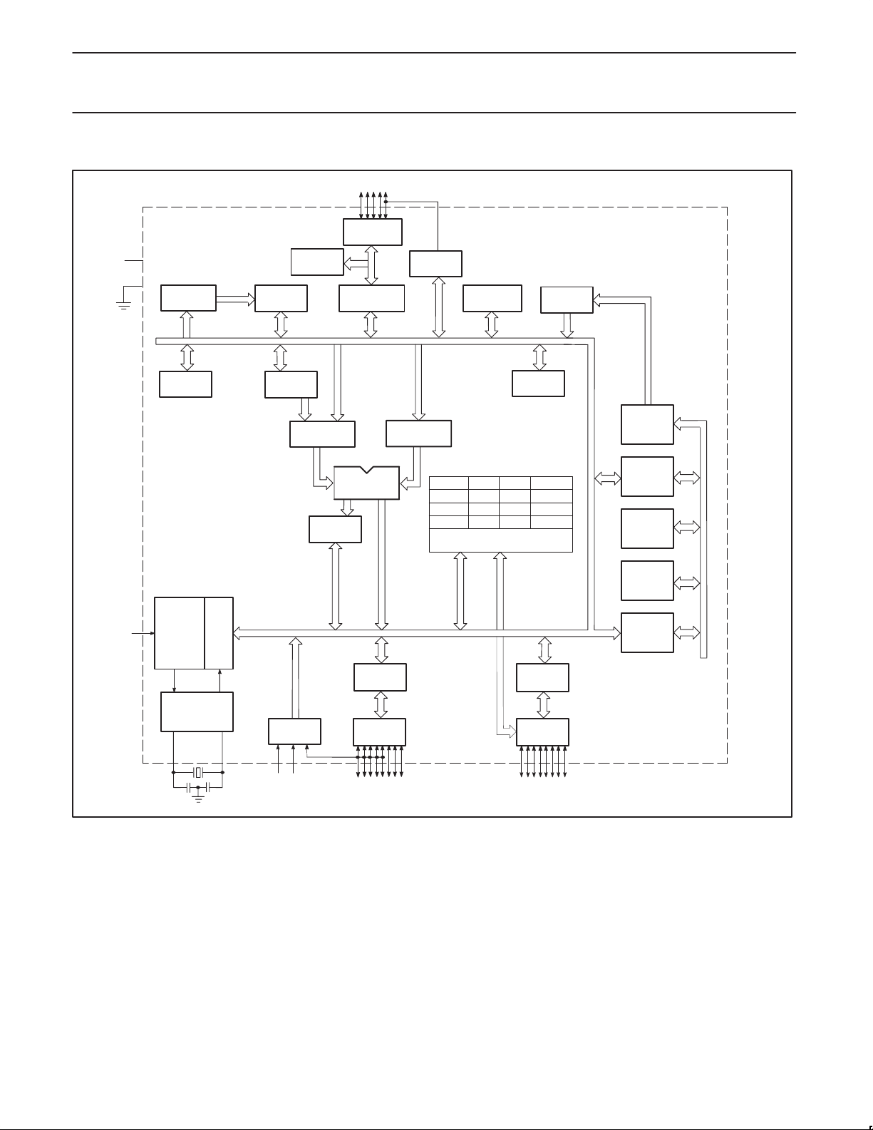
BLOCK DIAGRAM
P0.0–P0.4
PORT 0
DRIVERS
V
CC
V
SS
RAM ADDR
REGISTER
B
REGISTER
RAM
CONTROL
ACC
I2C
TMP2
PSW
PORT 0
LATCH
ALU
PWM
PORT 2
LATCH
TMP1
PCON I2CFG I2STA TCON
I2DAT I2CON IE
TH0 TL0
RTH RTL
INTERRUPT, SERIAL
PORT AND TIMER BLOCKS
STACK
POINTER
ROM/
EPROM
83C752/87C752
PROGRAM
ADDRESS
REGISTER
BUFFER
PC
INCRE-
MENTER
RST
TIMING
AND
CONTROL
OSCILLATOR
X1
INSTRUCTION
PD
REGISTER
X2
ADC
AVSSAV
PROGRAM
COUNTER
DPTR
PORT 1
LATCH
PORT 1
DRIVERS
CC
P1.0–P1.7
PORT 3
LATCH
PORT 3
DRIVERS
P3.0–P3.7
SU00319
1999 Jul 23
3

Philips Semiconductors Product specification
80C51 8-bit microcontroller family
2K/64 OTP/ROM, 5 channel 8 bit A/D, I2C, PWM, low pin count
PIN CONFIGURATIONS
P3.4/A4
P3.3/A3
P3.2/A2/A10
P3.1/A1/A9
P3.0/A0/A8
P0.2/V
P0.1/SDA/OE–PGM
P0.0/SCL/ASEL
RST
V
P1.0/ADC0/D0
P1.1/ADC1/D1
1
2
3
4
5
PLASTIC
DUAL
6
PP
X2
X1
SS
7
8
9
10
11
12
13
14
IN-LINE
PACKAGE
AND
SHRINK
SMALL
OUTLINE
PACKAGE
V
28
CC
P3.5/A5
27
P3.6/A6
26
P3.7/A7
25
P0.4/PWM OUT
24
P0.3
23
P1.7/T0/D7
22
21
P1.6/INT1
20
P1.5/INT0/D5
AV
19
CC
18
AV
SS
P1.4/ADC4/D4
17
16
P1.3/ADC3/D3
15
P1.2/ADC2/D2
/D6
83C752/87C752
5
11
Pin Function
1 P3.4/A4
2 P3.3/A3
3 P3.2/A2/A10
4 P3.1/A1/A9
5 P3.0/A0/A8
6 P0.2/V
7 P0.1/SDA/OE-PGM
8 P0.0/SCL/ASEL
9 RST
10 X2
11 X1
12 V
13 P1.0/ADC0/D0
14 P1.1/ADC1/D1
PP
SS
4126
PLASTIC
LEADED
CHIP
CARRIER
12 18
Pin Function
15 P1.2/ADC2/D2
16 P1.3/ADC3/D3
17 P1.4/ADC4/D4
18 AV
19 AV
20 P1.5/INT0/D5
21 P1.6/INT1
22 P1.7/T0/D7
23 P0.3
24 P0.4/PWM OUT
25 P3.7/A7
26 P3.6/A6
27 P3.5/A5
28 V
25
19
SS
CC
/D6
CC
SU00318
1999 Jul 23
4
Philips Semiconductors Product specification
80C51 8-bit microcontroller family
83C752/87C752
2K/64 OTP/ROM, 5 channel 8 bit A/D, I2C, PWM, low pin count
PIN DESCRIPTION
MNEMONIC PIN NO. TYPE NAME AND FUNCTION
V
SS
V
CC
P0.0–P0.4 8–6
P1.0–P1.7 13–17,
P3.0–P3.7 5–1,
RST 9 I Reset: A high on this pin for two machine cycles while the oscillator is running resets the device. An
X1 11 I Crystal 1: Input to the inverting oscillator amplifier and input to the internal clock generator circuits. X1
X2 10 O Crystal 2: Output from the inverting oscillator amplifier.
1
AV
CC
1
AV
SS
NOTE:
1. AV
(reference ground) must be connected to 0V (ground). AVCC (reference input) cannot differ from VCC by more than ±0.2V, and must be
SS
in the range 4.5V to 5.5V .
2. When P0.2 is at or close to 0V, it may affect the internal ROM operation. We recommend that P0.2 be tied to V
(e.g., 2kΩ).
12 I Circuit Ground Potential.
28 I Supply voltage during normal, idle, and power-down operation.
I/O Port 0: Port 0 is a 5-bit bidirectional port. Port 0.0–P0.2 are open drain. Port 0.0–P0.2 pins that have
23, 24
1s written to them float, and in that state can be used as high-impedance inputs. P0.3–P0.4 are
bidirectional I/O port pins with internal pull-ups. Port 0 also serves as the serial I
feature is activated by software, SCL and SDA are driven low in accordance with the I
2
C interface. When this
2
C protocol.
These pins are driven low if the port register bit is written with a 0 or if the I2C subsystem presents a 0.
The state of the pin can always be read from the port register by the program. Port 0.3 and 0.4 have
internal pull-ups that function identically to port 3. Pins that have 1s written to them are pulled high by
the internal pull-ups and can be used as inputs.
2
To comply with the I
C specification, P0.0 and P0.1 are open drain bidirectional I/O pins with the
electrical characteristics listed in the tables that follow. While these differ from “standard TTL”
characteristics, they are close enough for the pins to still be used as general-purpose I/O in non-I
applications.
6 I VPP (P0.2) – Programming voltage input. (See Note 2.)
7 I OE/PGM (P0.1) – Input which specifies verify mode (output enable) or the program mode.
OE/PGM = 1 output enabled (verify mode).
OE/PGM = 0 program mode.
8 I ASEL (P0.0) – Input which indicates which bits of the EPROM address are applied to port 3.
ASEL = 0 low address byte available on port 3.
ASEL = 1 high address byte available on port 3 (only the three least significant bits are used).
I/O Port 1: Port 1 is an 8-bit bidirectional I/O port with internal pull-ups. Port 1 pins that have 1s written to
20–22
them are pulled high by the internal pull-ups and can be used as inputs. P0.3–P0.4 pins are
bidirectional I/O port pins with internal pull-ups. As inputs, port 1 pins that are externally pulled low will
source current because of the internal pull-ups. (See DC Electrical Characteristics: I
serves the special function features of the P80C51 family as listed below:
). Port 1 also
IL
20 I INT0 (P1.5): External interrupt.
21 I INT1 (P1.6): External interrupt.
22 I T0 (P1.7): Timer 0 external input.
13–17 I ADC0 (P1.0)–ADC4 (P1.4): Port 1 also functions as the inputs to the five channel multiplexed A/D
converter. These pins can be used as outputs only if the A/D function has been disabled. These pins
can be used as inputs while the A/D converter is enabled.
Port 1 serves to output the addressed EPROM contents in the verify mode and accepts as inputs the
value to program into the selected address during the program mode.
I/O Port 3: Port 3 is an 8-bit bidirectional I/O port with internal pull-ups. Port 3 pins that have 1s written to
27–25
them are pulled high by the internal pull-ups and can be used as inputs. As inputs, port 3 pins that are
externally being pulled low will source current because of the pull-ups. (See DC Electrical
Characteristics: I
programmed (or verified). The 11-bit address is multiplexed into this port as specified by P0.0/ASEL.
). Port 3 also functions as the address input for the EPROM memory location to be
IL
internal diffused resistor to VSS permits a power-on RESET using only an external capacitor to VCC.
After the device is reset, a 10-bit serial sequence, sent LSB first, applied to RESET, places the device
in the programming state allowing programming address, data and V
or verification purposes. The RESET serial sequence must be synchronized with the X1 input.
to be applied for programming
PP
also serves as the clock to strobe in a serial bit stream into RESET to place the device in the
programming state.
19 I Analog supply voltage and reference input.
18 I Analog supply and reference ground.
via a small pull-up
CC
2
C
1999 Jul 23
5

Philips Semiconductors Product specification
80C51 8-bit microcontroller family
2K/64 OTP/ROM, 5 channel 8 bit A/D, I2C, PWM, low pin count
OSCILLA T OR CHARACTERISTICS
X1 and X2 are the input and output, respectively, of an inverting
amplifier which can be configured for use as an on-chip oscillator.
To drive the device from an external clock source, X1 should be
driven while X2 is left unconnected. There are no requirements on
the duty cycle of the external clock signal, because the input to the
internal clock circuitry is through a divide-by-two flip-flop. However,
minimum and maximum high and low times specified in the data
sheet must be observed.
IDLE MODE
The 8XC752 includes the 80C51 power-down and idle mode
features. In idle mode, the CPU puts itself to sleep while all of the
on-chip peripherals except the A/D and PWM stay active. The
functions that continue to run while in the idle mode are Timer 0, the
2
C interface including Timer I, and the interrupts. The instruction to
I
invoke the idle mode is the last instruction executed in the normal
operating mode before the idle mode is activated. The CPU
contents, the on-chip RAM, and all of the special function registers
remain intact during this mode. The idle mode can be terminated
either by any enabled interrupt (at which time the process is picked
up at the interrupt service routine and continued), or by a hardware
reset which starts the processor in the same manner as a power-on
reset. Upon powering-up the circuit, or exiting from idle mode,
sufficient time must be allowed for stabilization of the internal analog
reference voltages before an A/D conversion is started.
Special Function Registers
The special function registers (directly addressable only) contain all
of the 8XC751 registers except the program counter and the four
register banks. Most of the 21 special function registers are used to
control the on-chip peripheral hardware. Other registers include
arithmetic registers (ACC, B, PSW), stack pointer (SP) and data
pointer registers (DPH, DPL). Nine of the SFRs are bit addressable.
Data Pointer
The data pointer (DPTR) consists of a high byte (DPH) and a low
byte (DPL). In the 80C51 this register allows the access of external
data memory using the MOVX instruction. Since the 83C752 does
not support MOVX or external memory accesses, this register is
generally used as a 16-bit offset pointer of the accumulator in a
MOVC instruction. DPTR may also be manipulated as two
independent 8-bit registers.
DIFFERENCES BETWEEN THE 8XC752 AND
THE 80C51
Program Memory
On the 8XC752, program memory is 2048 bytes long and is not
externally expandable, so the 80C51 instructions MOVX, LJMP, and
LCALL are not implemented. If these instructions are executed, the
appropriate number of instruction cycles will take place along with
external fetches; however, no operation will take place. The LJMP
may not respond to all program address bits. The only fixed
locations in program memory are the addresses at which execution
is taken up in response to reset and interrupts, which are as follows:
Event Address
Reset 000
External INT0
Counter/timer 0 00B
External INT1 013
Timer I 01B
2
C serial 023
I
ADC 02B
PWM 033
Memory Organization
The 8XC752 manipulates operands in three memory address
spaces. The first is the program memory space which contains
program instructions as well as constants such as look-up tables.
The program memory space contains 2k bytes in the 8XC752.
The second memory space is the data memory array which has a
logical address space of 128 bytes. However, only the first 64 (0 to
3FH) are implemented in the 8XC752.
The third memory space is the special function register array having
a 128-byte address space (80H to FFH). Only selected locations in
this memory space are used (see Table 2). Note that the
architecture of these memory spaces (internal program memory,
internal data memory , and special function registers) is identical to
the 80C51, and the 8XC752 varies only in the amount of memory
physically implemented.
The 8XC752 does not directly address any external data or program
memory spaces. For this reason, the MOVX instructions in the
80C51 instruction set are not implemented in the 83C752, nor are
the alternate I/O pin functions RD
83C752/87C752
Program Memory
003
and WR.
POWER-DOWN MODE
In the power-down mode, the oscillator is stopped and the instruction
to invoke power-down is the last instruction executed. Only the
contents of the on-chip RAM are preserved. A hardware reset is the
only way to terminate the power-down mode. The control bits for the
reduced power modes are in the special function register PCON.
Table 1. External Pin Status During Idle and
Power-Down Modes
MODE Port 0* Port 1 Port 2
Idle Data Data Data
Power-down Data Data Data
* Except for PWM output (P0.4).
1999 Jul 23
6

Philips Semiconductors Product specification
80C51 8-bit microcontroller family
2K/64 OTP/ROM, 5 channel 8 bit A/D, I2C, PWM, low pin count
READ
LATCH
INT. BUS
WRITE TO
LATCH
READ
PIN
DQ
CL Q
I/O Ports
The I/O pins provided by the 83C752 consist of port 0, port 1, and
port 3.
Port 0
Port 0 is a 5-bit bidirectional I/O port and includes alternate functions
on some pins of this port. Pins P0.3 and P0.4 are provided with
internal pullups while the remaining pins (P0.0, P0.1, and P0.2) have
open drain output structures. The alternate functions for port 0 are:
2
P0.0 SCL – the I
P0.1 SDA – the I
P0.4 PWM – the PWM output
If the alternate functions, I
these pins may be used as I/O ports.
Port 1
Port 1 is an 8-bit bidirectional I/O port whose structure is identical to
the 80C51, but also includes alternate input functions on all pins.
The alternate pin functions for port 1 are:
P1.0-P1.4 - ADC0-ADC4 - A/D converter analog inputs
P1.5 INT0
P1.6 INT1
- external interrupt 0 input
- external interrupt 1 input
P1.7 - T0 - timer 0 external input
If the alternate functions INT0, INT1, or T0 are not being used, these
pins may be used as standard I/O ports. It is necessary to connect
and AVSS to VCC and VSS, respectively, in order to use these
AV
CC
pins as standard I/O pins. When the A/D converter is enabled, the
analog channel connected to the A/D may not be used as a digital
input; however, the remaining analog inputs may be used as digital
inputs. They may not be used as digital outputs. While the A/D is
enabled, the analog inputs are floating.
Port 3
Port 3 is an 8-bit bidirectional I/O port whose structure is identical to
the 80C51. Note that the alternate functions associated with port 3
of the 80C51 have been moved to port 1 of the 83C752 (as
applicable). See Figure 1 for port bit configurations.
C bus clock
2
C bus data
2
ALTERNATE
OUTPUT
FUNCTION
P1.X
LATCH
ALTERNATE INPUT
FUNCTION
V
DD
INTERNAL
PULL-UP
Figure 1. Port Bit Latches and I/O Buffers
C and PWM, are not being used, then
P1.X
PIN
READ
LATCH
INT. BUS
WRITE TO
LATCH
READ
PIN
Counter/Timer Subsystem
The 8XC752 has one counter/timer called timer/counter 0. Its
operation is similar to mode 2 operation on the 80C51, but is
extended to 16 bits with 16 bits of autoload. The controls for this
counter are centralized in a single register called TCON.
A watchdog timer, called Timer I, is for use with the I
2
C applications, this timer is dedicated to time-generation and
In I
bus monitoring of the I
use as a fixed time-base.
Interrupt Subsystem—Fixed Priority
The IP register and the 2-level interrupt system of the 80C51 are
eliminated. The interrupt structure is a seven-source, one-level
interrupt system similar to the 8XC751. Simultaneous interrupt
conditions are resolved by a single-level, fixed priority as follows:
Highest priority: Pin INT0
Lowest priority: ADC
The vector addresses are as follows:
Source Vector Address
INT0 0003H
TF0 000BH
INT1 0013H
TIMER I 001BH
SIO 0023H
ADC 002BH
PWM 0033H
Interrupt Control Registers
The 80C51 interrupt enable register is modified to take into account
the different interrupt sources of the 8XC752.
83C752/87C752
ALTERNATE
OUTPUT
FUNCTION
DQ
P0.X
LATCH
CL Q
ALTERNATE INPUT
FUNCTION
2
C subsystem.
2
C. In non-I2C applications, it is available for
Counter/timer flag 0
Pin INT1
PWM
Timer I
2
C
Serial I
P0.X
PIN
SU00306
1999 Jul 23
7

Philips Semiconductors Product specification
80C51 8-bit microcontroller family
2K/64 OTP/ROM, 5 channel 8 bit A/D, I2C, PWM, low pin count
Interrupt Enable Register
MSB LSB
EAD ETI ES EPWM EX1 ET0 EX0
EA
Position Symbol Function
IE.7 EA Global interrupt disable when EA = 0
IE.6 EAD A/D conversion complete
IE.5 ETI Timer I
IE.4 ES I
IE.3 EPWM PWM counter overflow
IE.2 EX1 External interrupt 1
IE.1 ET0 Timer 0 overflow
IE.0 EX0 External interrupt 0
2
C serial port
Serial Communications
The 8XC752 contains an I2C serial communications port instead of
the 80C51 UART. The I
interface with all of the hardware necessary to support multimaster
and slave operations. Also included are receiver digital filters and
timer (timer I) for communication watch-dog purposes. The I
serial port is controlled through four special function registers; I
2
control, I
The I
between devices connected to the bus. The main technical features
of the bus are:
C data, I2C status, and I2C configuration.
2
C bus uses two wires (SDA and SCL) to transfer information
2
C serial port is a single bit hardware
2
C
2
C
•Bidirectional data transfer between masters and slaves
•Serial addressing of slaves
•Acknowledgment after each transferred byte
•Multimaster bus
•Arbitration between simultaneously transmitting master without
corruption of serial data on bus
•With 82B715, communication distance is extended to beyond 100
feet (30M)
A large family of I
for more details on the bus and available ICs.
The 83C752 I
software required to drive the I
that on the 83C751. (See the 83C751 section for a detailed
discussion of this subsystem).
2
C compatible ICs is available. See the I2C section
2
C subsystem includes hardware to simplify the
2
C bus. This circuitry is the same as
Pulse Width Modulation Output (P0.4)
The PWM outputs pulses of programmable length and interval. The
repetition frequency is defined by an 8-bit prescaler which generates
the clock for the counter. The prescaler register is PWMP. The
prescaler and counter are not associated with any other timer. The
8-bit counter counts modulo 255, that is from 0 to 254 inclusive. The
value of the 8-bit counter is compared to the contents of a compare
register, PWM. When the counter value matches the contents of this
register, the output of the PWM is set high. When the counter reaches
zero, the output of the PWM is set low. The pulse width ratio (duty
cycle) is defined by the contents of the compare register and is in the
range of 0 to 1 programmed in increments of 1/255. The PWM output
can be set to be continuously high by loading the compare register
with 0 and the output can be set to be continuously low by loading the
compare register with 255. The PWM output is enabled by a bit in a
special function register, PWENA. When enabled, the pin output is
driven with a fully active pull-up. That is, when the output is high, a
strong pull-up is continuously applied. when disabled, the pin
functions as a normal bidirectional I/O pin, however, the counter
remains active.
The PWM function is disabled during RESET and remains disabled
after reset is removed until re-enabled by software. The PWM output
is high during power down and idle. The counter is disabled during
idle. The repetition frequency of the PWM is given by:
f
= f
PWM
OSC
The low/high ratio of the PWM signal is PWM / (255 – PWM) for
PWM not equal to 255. For PWM = 255, the output is always low.
The repetition frequency range is 92Hz to 23.5kHz for an oscillator
frequency of 12 MHz.
An interrupt will be asserted upon PWM counter overflow if the
interrupt is not masked off.
The PWM output is an alternative function of P0.4. In order to use
this port as a bidirectional I/O port, the PWM output must be
disabled by clearing the enable/disable bit in PWENA. In this case,
the PWM subsystem can be used as an interval timer by enabling
the PWM interrupt.
83C752/87C752
/ 2 (1 + PWMP) 255
1999 Jul 23
8
 Loading...