

Philips S87C751-1A28, S87C751-2A28 Datasheet

INTEGRATED CIRCUITS
83C751/87C751
80C51 8-bit microcontroller family
2K/64 OTP/ROM, I2C, low pin count
Product specification
Supersedes data of 1998 Jan 19
IC20 Data Handbook
1998 May 01

Philips Semiconductors Product specification
80C51 8-bit microcontroller family
2
2K/64 OTP/ROM, I
DESCRIPTION
The Philips 83C751/87C751 offers the advantages of the 80C51
architecture in a small package and at low cost.
The 8XC751 Microcontroller is fabricated with Philips high-density
CMOS technology. Philips epitaxial substrate minimizes CMOS
latch-up sensitivity.
The 8XC751 contains a 2k × 8 ROM (83C751) EPROM (87C751), a
64 × 8 RAM, 19 I/O lines, a 16-bit auto-reload counter/timer, a
five-source, fixed-priority level interrupt structure, a bidirectional
inter-integrated circuit (I
oscillator.
The on-board inter-integrated circuit (I
8XC751 to operate as a master or slave device on the I
area network. This capability facilitates I/O and RAM expansion,
access to EEPROM, processor-to-processor communication, and
efficient interface to a wide variety of dedicated I
FEA TURES
•80C51 based architecture
•Inter-Integrated Circuit (I
•Small package sizes
– 24-pin DIP (300 mil “skinny DIP”)
– 24-pin Shrink Small Outline Package
– 28-pin PLCC
•87C751 available in one-time programmable plastic packages
•Wide oscillator frequency range
•Low power consumption:
– Normal operation: less than 11mA @ 5V, 12MHz
– Idle mode
– Power-down mode
•2k × 8 ROM (83C751)
2k × 8 EPROM (87C751)
•64 × 8 RAM
•16-bit auto reloadable counter/timer
•Fixed-rate timer
•Boolean processor
•CMOS and TTL compatible
•Well suited for logic replacement, consumer and industrial
applications
•LED drive outputs
2
C) serial bus interface, and an on-chip
2
C) serial bus interface
C, low pin count
2
C) bus interface allows the
2
C small
2
C peripherals.
PIN CONFIGURATIONS
P3.4/A4
1
P3.3/A3
2
RST
V
X2
X1
SS
PP
10
11
12
5
11
3
4
5
6
7
8
9
12 18
PinFunction
P3.2/A2/A10
P3.1/A1/A9
P3.0/A0/A8
P0.2/V
P0.1/SDA/OE–PGM
P0.0/SCL/ASEL
Pin Function
1 P3.4/A4
2 P3.3/A3
3 P3.2/A2/A10
4 P3.1/A1/A9
5 NC*
6 P3.0/A0/A8
7 P0.2/V
8 P0.1/SDA/OE-PGM
9 P0.0//SCLASEL
* DO NOT CONNECT
PP
83C751/87C751
24
V
CC
P3.5/A5
23
22
P3.6/A6
21
PLASTIC
DUAL
IN-LINE
PACKAGE
AND
SHRINK
SMALL
OUTLINE
PACKAGE
4126
PLASTIC
LEADED
CHIP
CARRIER
10 NC*
11 RST
12 X2
13 X1
14 V
SS
15 P1.0/D0
16 P1.1/D1
17 P1.2/D2
18 P1.3/D3
P3.7/A7
20
P1.7/T0/D7
P1.6/INT1
19
18
P1.5/INT0/D5
17
P1.4/D4
16
P1.3/D3
15
P1.2/D2
14
P1.1/D1
13
P1.0/D0
25
19
Pin Function
/D6
19 P1.4/D4
20 P1.5/INT0
21 NC*
22 NC*
23 P1.6/INT1
24 P1.7/T0/D7
25 P3.7/A7
26 P3.6/A6
27 P3.5/A5
28 V
CC
/D5
/D6
SU00315
1998 May 01 853-0599 19326
2

Philips Semiconductors Product specification
80C51 8-bit microcontroller family
2
2K/64 OTP/ROM, I
C, low pin count
83C751/87C751
ORDERING INFORMATION
ROM EPROM
S83C751–1N24 S87C751–1N24 OTP 0 to +70, Plastic Dual In-line Package 3.5 to 12MHz SOT222-1
S83C751–2N24 S87C751–2N24 OTP –40 to +85, Plastic Dual In-line Package 3.5 to 12MHz SOT222-1
S83C751–4N24 S87C751–4N24 OTP 0 to +70, Plastic Dual In-line Package 3.5 to 16MHz SOT222-1
S83C751–5N24 S87C751–5N24 OTP –40 to +85, Plastic Dual In-line Package 3.5 to 16MHz SOT222-1
S83C751–1A28 S87C751–1A28 OTP 0 to +70, Plastic Leaded Chip Carrier 3.5 to 12MHz SOT261-3
S83C751–2A28 S87C751–2A28 OTP –40 to +85, Plastic Leaded Chip Carrier 3.5 to 12MHz SOT261-3
S83C751–4A28 S87C751–4A28 OTP 0 to +70, Plastic Leaded Chip Carrier 3.5 to 16MHz SOT261-3
S83C751–5A28 S87C751–5A28 OTP –40 to +85, Plastic Leaded Chip Carrier 3.5 to 16MHz SOT261-3
S83C751–1DB S87C751–1DB OTP 0 to +70, Shrink Small Outline Package 3.5 to 12MHz SOT340-1
S83C751–4DB S87C751–4DB OTP 0 to +70, Shrink Small Outline Package 3.5 to 16MHz SOT340-1
NOTE:
1. OTP = One Time Programmable EPROM.
1
TEMPERATURE RANGE °C
AND PACKAGE
FREQUENCY
DRAWING
NUMBER
1998 May 01
3
Philips Semiconductors Product specification
80C51 8-bit microcontroller family
2
2K/64 OTP/ROM, I
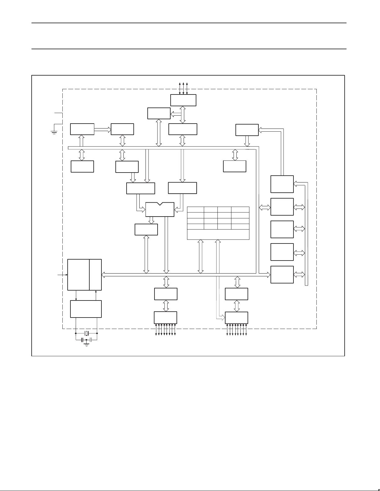
BLOCK DIAGRAM
V
CC
V
SS
RAM ADDR
REGISTER
B
REGISTER
C, low pin count
RAM
ACC
TMP2
PSW
I2C
CONTROL
ALU
P0.0–P0.2
PORT 0
DRIVERS
PORT 0
LATCH
TMP1
PCON I2CFG I2STA TCON
I2DAT I2CON IE
TH0 TL0
RTH RTL
INTERRUPT, SERIAL
PORT AND TIMER BLOCKS
STACK
POINTER
ROM/
EPROM
83C751/87C751
PROGRAM
ADDRESS
REGISTER
BUFFER
PC
INCRE-
MENTER
RST
TIMING
AND
CONTROL
OSCILLATOR
X1
INSTRUCTION
PD
REGISTER
X2
PORT 1
LATCH
PORT 1
DRIVERS
P1.0–P1.7
PORT 3
LATCH
PORT 3
DRIVERS
P3.0–P3.7
PROGRAM
COUNTER
DPTR
SU00316
1998 May 01
4
Philips Semiconductors Product specification
80C51 8-bit microcontroller family
2
2K/64 OTP/ROM, I
C, low pin count
83C751/87C751
PIN DESCRIPTIONS
PIN NO.
MNEMONIC
V
SS
V
CC
P0.0–P0.2 8–6 9–7 I/O Port 0: Port 0 is a 3-bit open-drain, bidirectional port. Port 0 pins that have 1s written to them float,
P1.0–P1.7 13–20 15–20,
P3.0–P3.7 5–1,
RST 9 11 I Reset: A high on this pin for two machine cycles while the oscillator is running, resets the device.
X1 11 13 I Crystal 1: Input to the inverting oscillator amplifier and input to the internal clock generator circuits.
X2 10 12 O Crystal 2: Output from the inverting oscillator amplifier.
NOTE:
1. When P0.2 is at or close to 0V it may affect the internal ROM operation. We recommend that P0.2 be tied to V
(e.g., 2kΩ).
DIP/
SSOP
23–21
LCC TYPE NAME AND FUNCTION
12 14 I Circuit Ground Potential
24 28 I Supply voltage during normal, idle, and power-down operation.
and in that state can be used as high-impedance inputs. Port 0 also serves as the serial I2C
interface. When this feature is activated by software, SCL and SDA are driven low in accordance
with the I
subsystem presents a 0. The state of the pin can always be read from the port register by the
program.
To comply with the I2C specification, P0.0 and P0.1 are open drain bidirectional I/O pins with the
electrical characteristics listed in the tables that follow. While these differ from “standard TTL”
characteristics, they are close enough for the pins to still be used as general-purpose I/O in
non-I
memory as follows:
6 7 N/A VPP (P0.2) – Programming voltage input. (See Note 1.)
7 8 I OE/PGM (P0.1) – Input which specifies verify mode (output enable) or the program mode.
8 9 I ASEL (P0.0) – Input which indicates which bits of the EPROM address are applied to port 3.
7 8 I/O SDA (P0.1) – I2C data.
8 9 I/O SCL (P0.0) – I2C clock.
23, 24
18 20 I INT0 (P1.5): External interrupt.
19 23 I INT1 (P1.6): External interrupt.
20 24 I T0 (P1.7): Timer 0 external input.
6, 4–1,
27–25
OE/PGM = 1 output enabled (verify mode).
OE/PGM = 0 program mode.
ASEL = 0 low address byte available on port 3.
ASEL = 1 high address byte available on port 3 (only the three least significant bits are used).
I/O Port 1: Port 1 is an 8-bit bidirectional I/O port with internal pull-ups. Port 1 pins that have 1s written
to them are pulled high by the internal pull-ups and can be used as inputs. As inputs, port 1 pins
that are externally pulled low will source current because of the internal pull-ups. (See DC
Electrical Characteristics: I
mode and accepts as inputs the value to program into the selected address during the program
mode. Port 1 also serves the special function features of the 80C51 family as listed below:
I/O Port 3: Port 3 is an 8-bit bidirectional I/O port with internal pull-ups. Port 3 pins that have 1s written
to them are pulled high by the internal pull-ups and can be used as inputs. As inputs, port 3 pins
that are externally being pulled low will source current because of the pull-ups. (See DC Electrical
Characteristics: I
be programmed (or verified). The 11-bit address is multiplexed into this port as specified by
P0.0/ASEL.
An internal diffused resistor to VSS permits a power-on RESET using only an external capacitor to
V
the device in the programming state allowing programming address, data and V
programming or verification purposes. The RESET serial sequence must be synchronized with the
X1 input.
X1 also serves as the clock to strobe in a serial bit stream into RESET to place the device in the
programming state.
2
C protocol. These pins are driven low if the port register bit is written with a 0 or if the I2C
2
C applications. Port 0 also provides alternate functions for programming the EPROM
). Port 1 serves to output the addressed EPROM contents in the verify
IL
). Port 3 also functions as the address input for the EPROM memory location to
IL
. After the device is reset, a 10-bit serial sequence, sent LSB first, applied to RESET, places
CC
via a small pullup
CC
to be applied for
PP
1998 May 01
5
Philips Semiconductors Product specification
SYMBOL
PARAMETER
TEST CONDITIONS
UNIT
80C51 8-bit microcontroller family
2
2K/64 OTP/ROM, I
ABSOLUTE MAXIMUM RATINGS
C, low pin count
1, 2
PARAMETER
83C751/87C751
RATING UNIT
Storage temperature range –65 to +150 °C
Voltage from V
Voltage from any pin to V
CC
to V
SS
(except VPP) –0.5 to VCC + 0.5 V
SS
–0.5 to +6.5 V
Power dissipation 1.0 W
Voltage on VPP pin to V
SS
0 to +13.0 V
Maximum IOL per I/O pin 10 mA
NOTES:
1. Stresses above those listed under Absolute Maximum Ratings may cause permanent damage to the device. This is a stress rating only and
functional operation of the device at these or any conditions other than those described in the AC and DC Electrical Characteristics section
of this specification is not implied.
2. This product includes circuitry specifically designed for the protection of its internal devices from the damaging effects of excessive static
charge. Nonetheless, it is suggested that conventional precautions be taken to avoid applying greater than the rated maxima.
DC ELECTRICAL CHARACTERISTICS
T
= 0°C to +70°C or –40°C to +85°C, VCC = 5V ±10% for 87C751, VCC = 5V ±10% for 83C751, VSS = 0V
amb
V
IL
V
IH
V
IH1
Input low voltage, except SDA, SCL –0.5 0.2VDD–0.1 V
Input high voltage, except X1, RST 0.2VCC+0.9 VCC+0.5 V
Input high voltage, X1, RST 0.7V
SDA, SCL, P0.2
V
IL1
V
IH2
V
OL
V
OL1
V
OH
Input low voltage –0.5 0.3V
Input high voltage 0.7V
Output low voltage, ports 1 and 3 IOL = 1.6mA
Output low voltage, port 0.2 IOL = 3.2mA
2
2
Output high voltage, ports 1 and 3 IOH = –60µA 2.4 V
IOH = –25µA 0.75V
IOH = –10µA 0.9V
Port 0.0 and 0.1 (I2C) – Drivers
V
OL2
Output low voltage IOL = 3mA 0.4 V
Driver, receiver combined: (over VCC range)
C Capacitance 10 pF
I
IL
I
TL
I
LI
R
RST
C
IO
I
PD
Logical 0 input current, ports 1 and 3 VIN = 0.45V –50 µA
Logical 1 to 0 transition current, ports 1 and 3
3
VIN = 2V (0 to 70°C)
VIN = 2V (–40 to +85°C)
Input leakage current, port 0 0.45 < VIN < V
CC
Internal pull-down resistor 25 175 kΩ
Pin capacitance
Power-down current
4
Test freq = 1MHz,
T
= 25°C
amb
VCC = 2 to VCC max 50 µA
VSS = 0V
V
PP
I
PP
I
CC
VPP program voltage (for 87C751 only)
Program current (for 87C751 only) VPP = 13.0V 50 mA
Supply current (see Figure 2)
VCC = 5V±10%
T
= 21°C to 27°C
amb
NOTES TO DC ELECTRICAL CHARACTERISTICS ON NEXT PAGE.
1
LIMITS
MIN MAX
CC
CC
VCC+0.5 V
CC
VCC+0.5 V
0.45 V
0.45 V
CC
CC
–650
–750
±10 µA
10 pF
12.5 13.0 V
V
V
V
µA
µA
1998 May 01
6

Philips Semiconductors Product specification
80C51 8-bit microcontroller family
2
2K/64 OTP/ROM, I
C, low pin count
83C751/87C751
NOTES TO DC ELECTRICAL CHARACTERISTICS:
1. Parameters are valid over operating temperature range unless otherwise specified. All voltages are with respect to V
noted.
2. Under steady state (non-transient) conditions, I
Maximum I
Maximum I
Maximum total I
If I
exceeds the test condition, VOL may exceed the related specification. Pins are not guaranteed to sink current greater than the listed
OL
test conditions.
per port pin: 10mA (NOTE: This is 85°C spec.)
OL
per 8-bit port: 26mA
OL
for all outputs: 67mA
OL
must be externally limited as follows:
OL
unless otherwise
SS
3. Pins of ports 1 and 3 source a transition current when they are being externally driven from 1 to 0. The transition current reaches its
maximum value when V
4. Power-down I
5. Active I
RST = port 0 = V
6. Idle I
CC
port 0 = V
CC
is measured with all output pins disconnected; X1 driven with t
CC
is measured with all output pins disconnected; X1 driven with t
; RST = VSS.
CC
is measured with all output pins disconnected; port 0 = VCC; X2, X1 n.c.; RST = VSS.
CC
is approximately 2V .
IN
. ICC will be slightly higher if a crystal oscillator is used.
CLCH
CLCH
, t
, t
= 5ns, VIL = VSS + 0.5V, VIH = VCC – 0.5V; X2 n.c.;
CHCL
= 5ns, VIL = VSS + 0.5V, VIH = VCC – 0.5V; X2 n.c.;
CHCL
AC ELECTRICAL CHARACTERISTICS
T
= 0°C to +70°C or –40°C to +85°C, VCC = 5V ±10% for 87C751, VCC = 5V ±10% for 83C751, VSS = 0V
amb
12MHz CLOCK VARIABLE CLOCK
SYMBOL PARAMETER MIN MAX MIN MAX UNIT
1/t
CLCL
Oscillator frequency: 3.5 12 MHz
External Clock (Figure 1)
t
CHCX
t
CLCX
t
CLCH
t
CHCL
High time 20 20 ns
Low time 20 20 ns
Rise time 20 20 ns
Fall time 20 20 ns
NOTES:
1. Parameters are valid over operating temperature range unless otherwise specified. All voltages are with respect to V
noted.
2. Load capacitance for ports = 80pF.
1, 2
3.5 16 MHz
unless otherwise
SS
1998 May 01
7

Philips Semiconductors Product specification
80C51 8-bit microcontroller family
2
2K/64 OTP/ROM, I
EXPLANATION OF THE AC SYMBOLS
Each timing symbol has five characters. The first character is always
‘t’ (= time). The other characters, depending on their positions,
indicate the name of a signal or the logical status of that signal. The
designations are:
C – Clock
D – Input data
H – Logic level high
L – Logic level low
Q – Output data
T – Time
V – V alid
X – No longer a valid logic level
Z – Float
VCC –0.5
0.45V
C, low pin count
+ 0.9
0.2 V
CC
– 0.1
0.2 V
CC
Figure 1. External Clock Drive
t
CHCL
t
CLCX
t
CLCL
t
CLCH
t
CHCX
83C751/87C751
SU00297
22
20
18
16
14
I
(mA)
CC
12
10
8
6
4
2
4MHz 8MHz 12MHz 16MHz
FREQ
Figure 2. ICC vs. FREQ
Maximum I
values taken at VCC max and worst case temperature.
CC
Typical I
values taken at VCC = 5.0V and 25°C.
CC
Notes 5 and 6 refer to DC Electrical Characteristics.
MAX ACTIVE I
TYP ACTIVE I
MAX IDLE I
TYP IDLE I
CC
CC
SU00298
CC
6
CC
6
5
5
1998 May 01
8
 Loading...