

Philips PXTA42 Datasheet
DISCRETE SEMICONDUCTORS
DATA SH EET
ook, halfpage
M3D109
PXTA42
NPN high-voltage transistor
Product specification
Supersedes data of 1997 Jun 18
1999 Apr 26
Philips Semiconductors Product specification
NPN high-voltage transistor PXTA42
FEATURES
• Low current (max. 100 mA)
PINNING
PIN DESCRIPTION
• High voltage (max. 300 V).
APPLICATIONS
• Telephony and professional communication equipment.
DESCRIPTION
handbook, halfpage
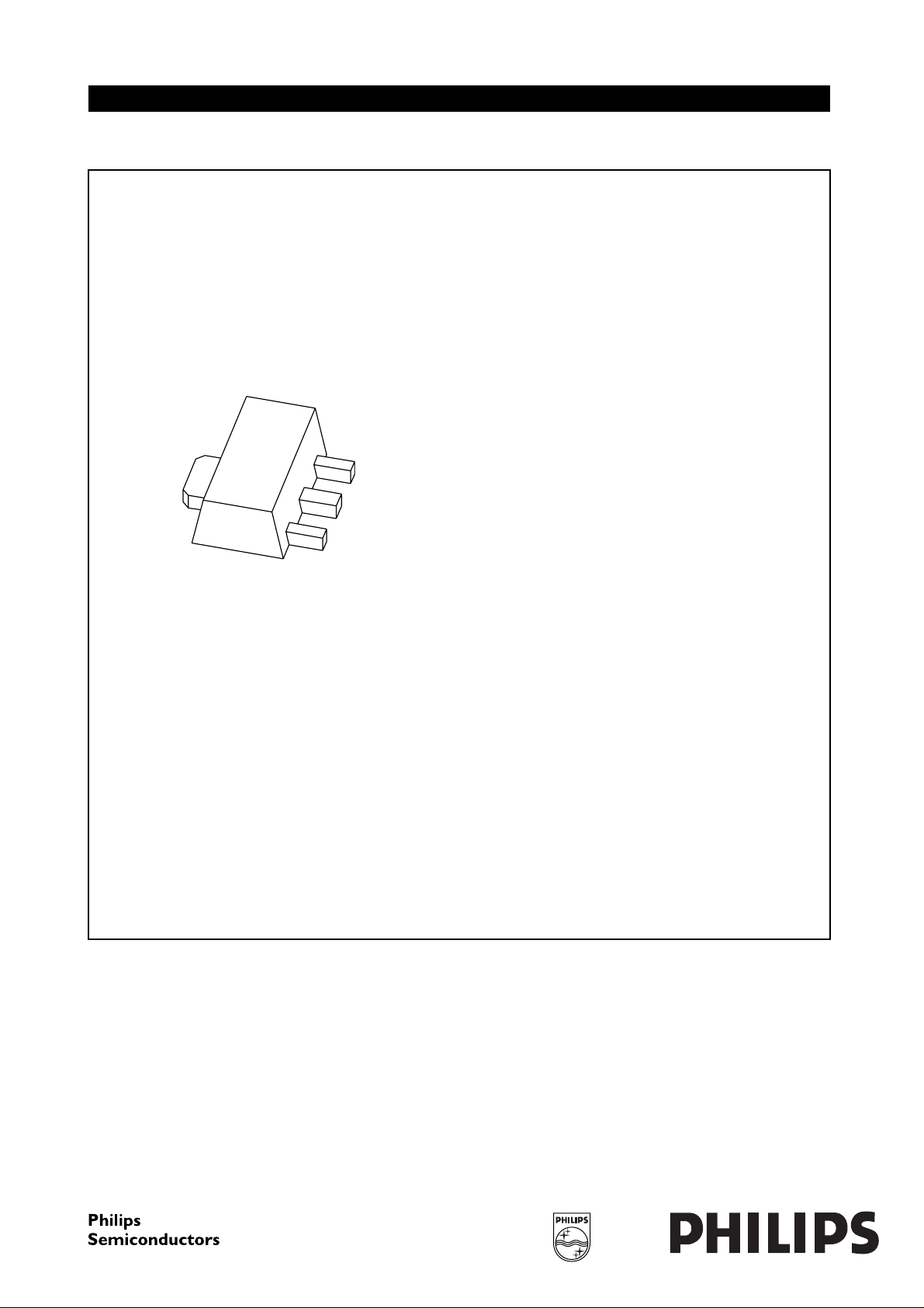
NPN high-voltage transistor in a SOT89 plastic package.
PNP complement: PXTA92.
MARKING
TYPE NUMBER MARKING CODE
PXTA42 p1D
LIMITING VALUES
In accordance with the Absolute Maximum Rating System (IEC 134).
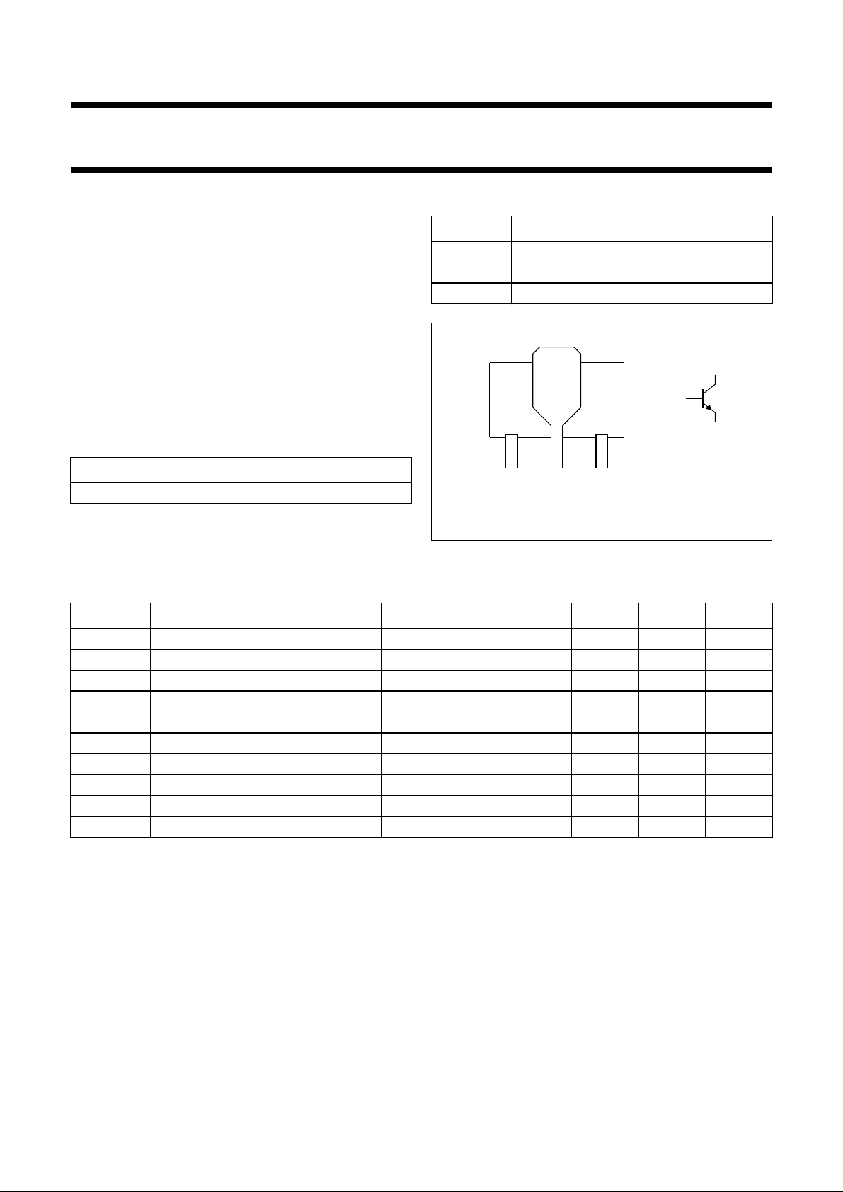
1 emitter
2 collector
3 base
2
3
1
123
Bottom view
MAM296
Fig.1 Simplified outline (SOT89) and symbol.
SYMBOL P ARAMETER CONDITIONS MIN. MAX. UNIT
V
CBO
V
CEO
V
EBO
I
C
I
CM
I
BM
P
tot
T
stg
T
j
T
amb
collector-base voltage open emitter − 300 V
collector-emitter voltage open base − 300 V
emitter-base voltage open collector − 6V
collector current (DC) − 100 mA
peak collector current − 200 mA
peak base current − 100 mA
total power dissipation T
≤ 25 °C; note 1 − 1.3 W
amb
storage temperature −65 +150 °C
junction temperature − 150 °C
operating ambient temperature −65 +150 °C
Note
1. Device mounted on a printed-circuit board, single-sided copper, tinplated, mounting pad for collector 6 cm
For other mounting conditions, see
“Thermal considerations for SOT89 in the General Part of associated Handbook”
2
.
.
1999 Apr 26 2
Philips Semiconductors Product specification
NPN high-voltage transistor PXTA42
THERMAL CHARACTERISTICS
SYMBOL PARAMETER CONDITIONS VALUE UNIT
R
th j-a
R
th j-s
Note
1. Device mounted on a printed-circuit board, single-sided copper, tinplated, mounting pad for collector 6 cm2.
For other mounting conditions, see
CHARACTERISTICS
=25°C unless otherwise specified.
T
amb
SYMBOL PARAMETER CONDITIONS MIN. MAX. UNIT
I
CBO
I
EBO
h
FE
V
CEsat
V
BEsat
C
re
f
T
thermal resistance from junction to ambient note 1 96 K/W
thermal resistance from junction to soldering point 16 K/W
“Thermal considerations for SOT89 in the General Part of associated Handbook”
collector cut-off current IE= 0; VCB= 200 V − 100 nA
emitter cut-off current IC= 0; VBE=6V − 100 nA
DC current gain IC= 1 mA; VCE=10V 25 −
I
= 10 mA; VCE=10V 40 −
C
= 30 mA; VCE=10V 40 −
I
C
collector-emitter saturation voltage IC= 20 mA; IB=2mA − 500 mV
base-emitter saturation voltage IC= 20 mA; IB=2mA − 900 mV
feedback capacitance IC=ic= 0; VCB= 20 V; f = 1 MHz − 3pF
transition frequency IC= 10 mA; VCE=20V;
50 − MHz
f = 100 MHz
.
1999 Apr 26 3
 Loading...