

Philips PXTA27 Datasheet
DISCRETE SEMICONDUCTORS
DATA SH EET
ook, halfpage
M3D109
PXTA27
NPN Darlington transistor
Product specification
Supersedes data of September 1994
1997 May 14
File under Discrete Semiconductors, SC04
Philips Semiconductors Product specification
NPN Darlington transistor PXTA27
FEATURES
• High current (max. 0.5 A)
• Low voltage (max. 60 V).
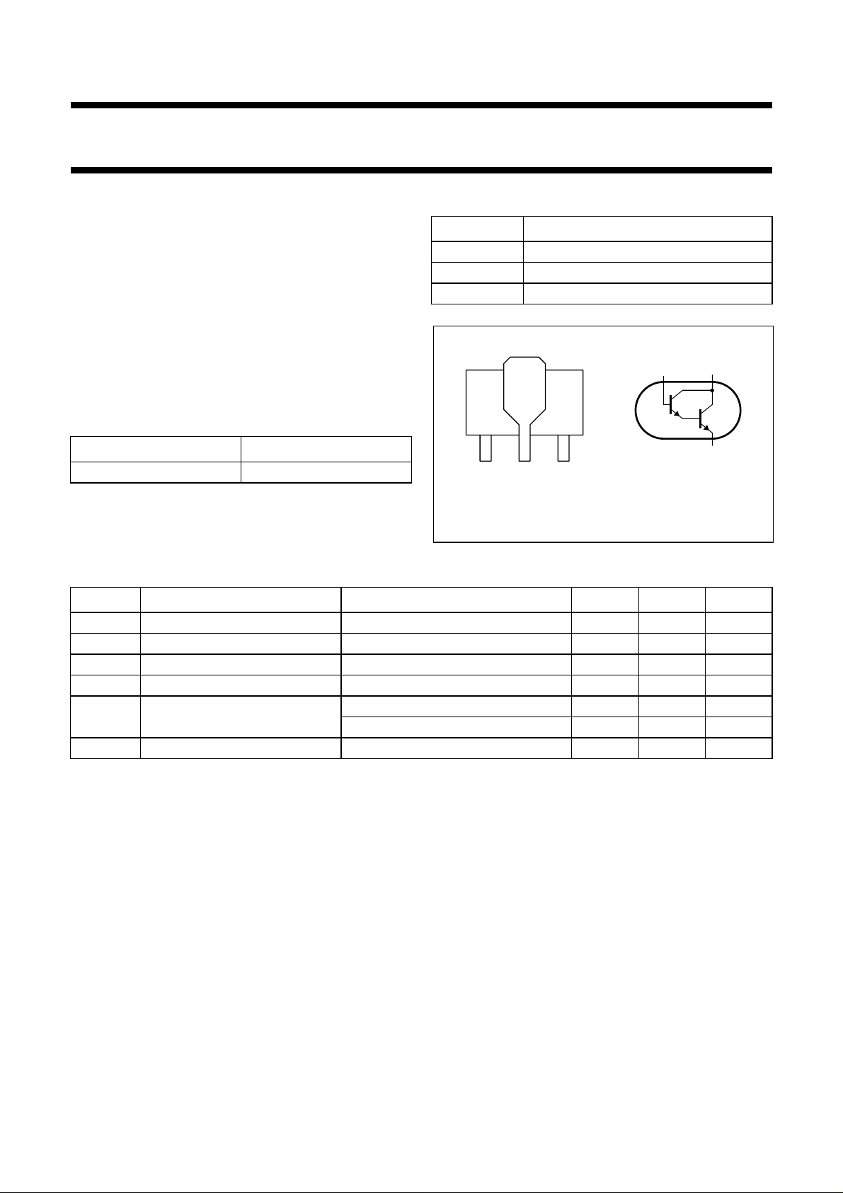
PINNING
PIN DESCRIPTION
1 emitter
2 collector
APPLICATIONS
3 base
• High input impedance preamplifiers.
DESCRIPTION
handbook, halfpage
32
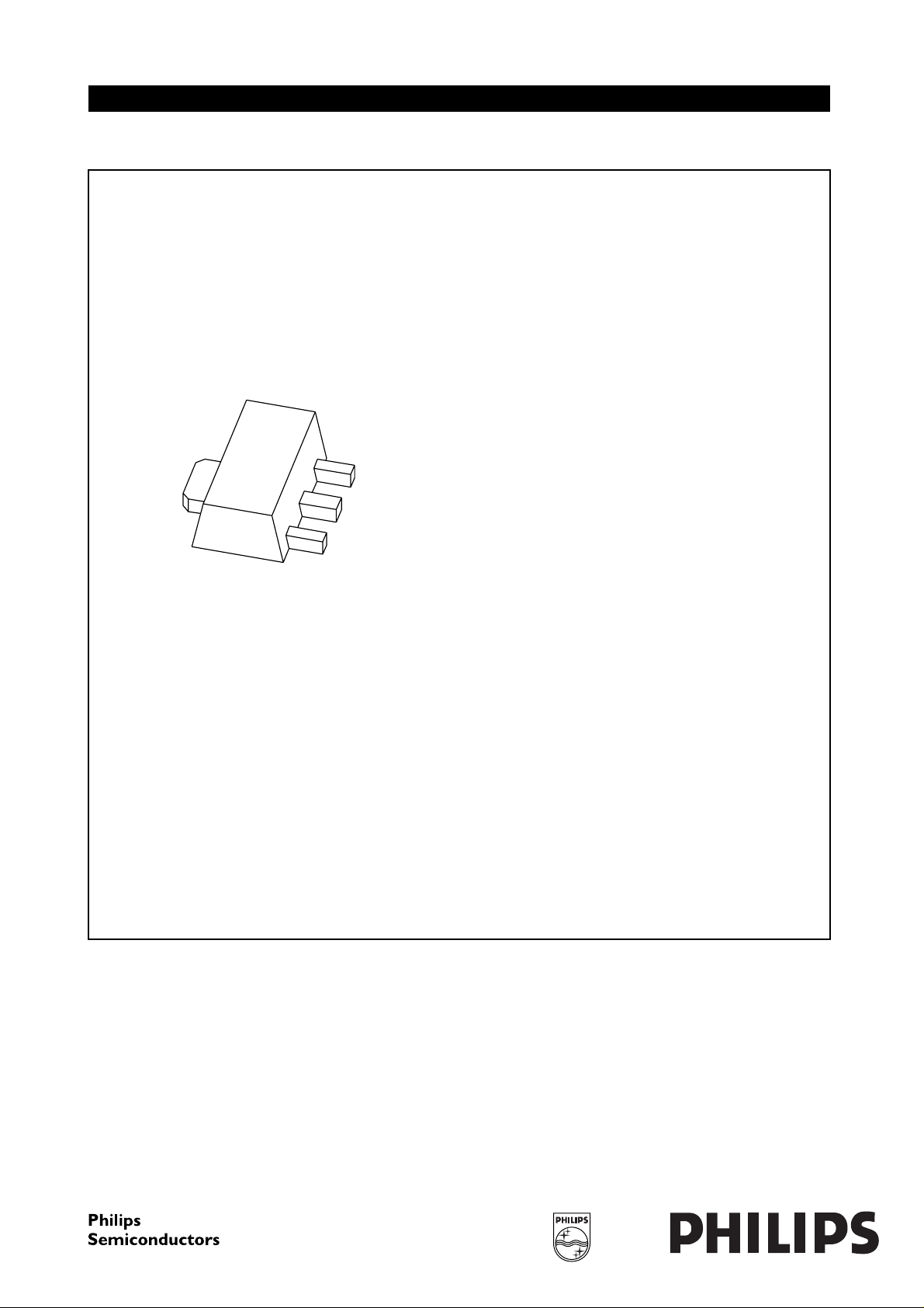
NPN Darlington transistor in a SOT89 plastic package.
TR1
MARKING
TYPE NUMBER MARKING CODE
PXTA27 A27
123
Bottom view
TR2
1
MAM300
Fig.1 Simplified outline (SOT89) and symbol.
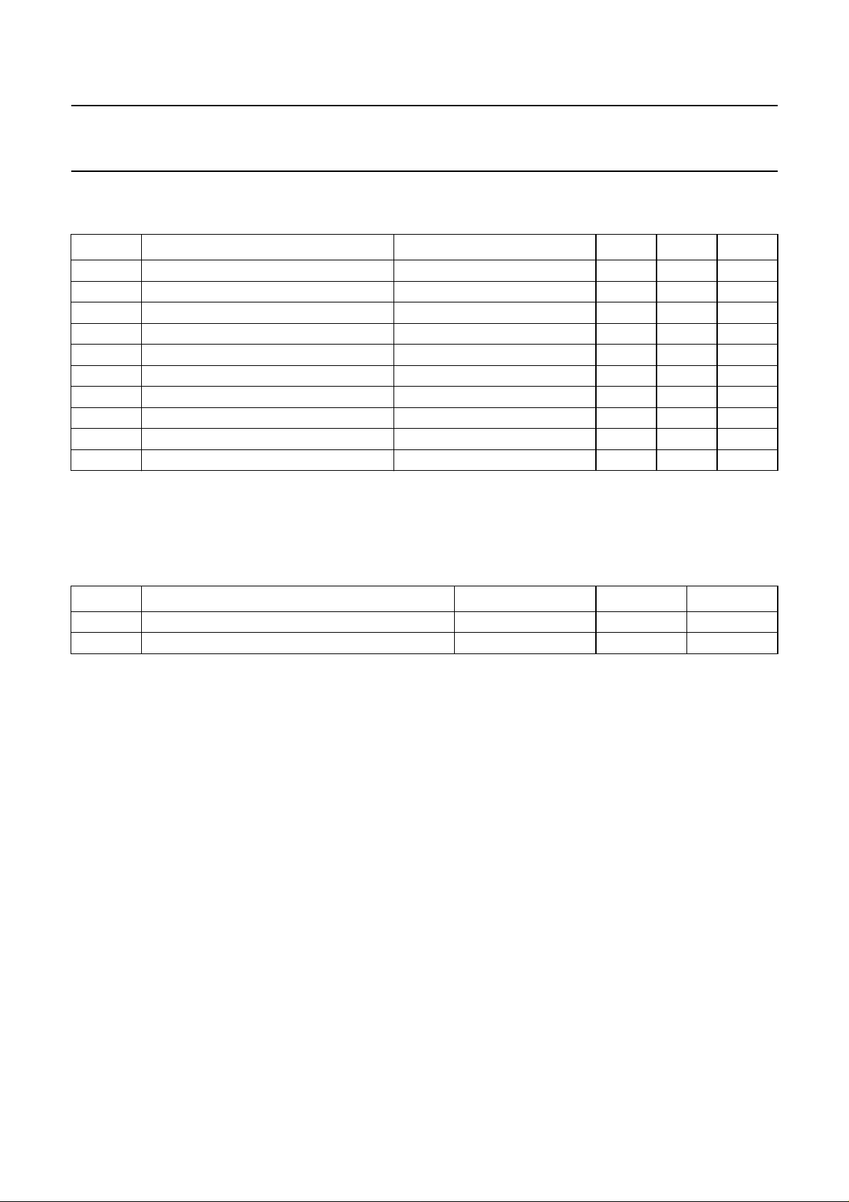
QUICK REFERENCE DATA
SYMBOL PARAMETER CONDITIONS MIN. MAX. UNIT
V
V
I
P
h
f
CBO
CES
C
tot
FE
T
collector-base voltage open emitter − 60 V
collector-emitter voltage VBE=0 − 60 V
collector current (DC) − 0.5 A
total power dissipation T
≤ 25 °C − 1.3 W
amb
DC current gain IC= 10 mA; VCE= 5 V 10000 −
I
= 100 mA; VCE= 5 V 10000 −
C
transition frequency IC= 30 mA; VCE= 5 V; f = 100 MHz 125 − MHz
1997 May 14 2
Philips Semiconductors Product specification
NPN Darlington transistor PXTA27
LIMITING VALUES
In accordance with the Absolute Maximum Rating System (IEC 134).
SYMBOL PARAMETER CONDITIONS MIN. MAX. UNIT
V
CBO
V
CES
V
EBO
I
C
I
CM
I
B
P
tot
T
stg
T
j
T
amb
Note
1. Device mounted on a printed-circuit board, single sided copper, tinplated, mounting pad for collector 1 cm
For other mounting conditions, see
collector-base voltage open emitter − 60 V
collector-emitter voltage VBE=0 − 60 V
emitter-base voltage open collector − 10 V
collector current (DC) − 0.5 A
peak collector current − 1A
base current (DC) − 200 mA
total power dissipation T
≤ 25 °C; note 1 − 1.3 W
amb
storage temperature −65 +150 °C
junction temperature − 150 °C
operating ambient temperature −65 +150 °C
2
.
“Thermal considerations for the SOT89 in the General part of handbook SC04”
.
THERMAL CHARACTERISTICS
SYMBOL PARAMETER CONDITIONS VALUE UNIT
R
R
th j-a
th j-s
thermal resistance from junction to ambient note 1 93 K/W
thermal resistance from junction to soldering point 12 K/W
Note
1. Device mounted on a printed-circuit board, single sided copper, tinplated, mounting pad for collector 1 cm
For other mounting conditions, see
“Thermal considerations for the SOT89 in the General part of handbook SC04”
2
.
.
1997 May 14 3
 Loading...