

Philips PVB42004X Datasheet

DISCRETE SEMICONDUCTORS
DATA SH EET
PVB42004X
NPN microwave power transistor
Product specification
Supersedes data of June 1992
File under Discrete Semiconductors, SC15
1997 Feb 19
Philips Semiconductors Product specification
NPN microwave power transistor PVB42004X
FEATURES
• Interdigitated structure provides high emitter efficiency
• Diffused emitter ballasting resistors providing excellent
current sharing and withstanding a high VSWR
• Local thick oxide and gold sandwich metallization
realizes very stable characteristics and excellent lifetime
• Multicell geometry gives good balance of dissipated
power and low thermal resistance.
APPLICATIONS
• Intended for use in common base class-B power
amplifiers up to 4.2 GHz.
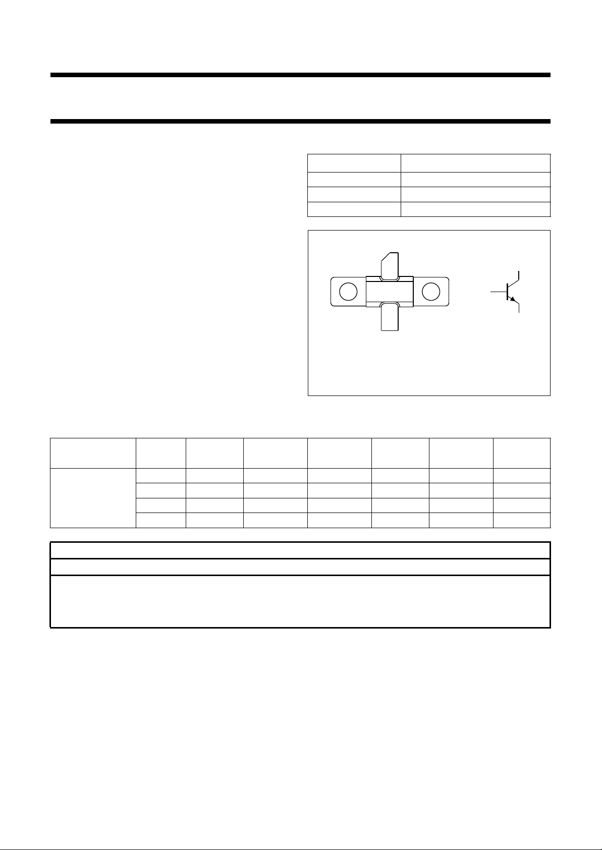
DESCRIPTION
NPN silicon planar epitaxial microwave power transistor in
a 2-lead rectangular flange package with a ceramic cap
(SOT445A) with the common base connected to the
flange.
QUICK REFERENCE DATA
Microwave performance up to T
=25°C in a common base class-B test circuit.
mb
PINNING - SOT445A
PIN DESCRIPTION
1 collector
2 emitter
3 base connected to flange
handbook, halfpage
33
Top view
1
2
Fig.1 Simplified outline and symbol.
c
b
e
MAM251
MODE OF
OPERATION
f
(GHz)
V
(V)
CC
P
(W)
L
G
p
(dB)
η
(%)
C
Z
i
(Ω)
Z
(Ω)
L
1 24 typ. 13 typ. 11 typ. 60 2.3 + j2.8 7.8 + j11.6
Class-B (CW)
2 24 typ. 10 typ. 10 typ. 48 1.4 + j9.5 3.9 + j2.6
3 24 typ. 7.5 typ. 8.8 typ. 30 4.2 + j21 2.3 − j2.5
4 24 typ. 4 typ. 6 typ. 25 38 − j32 1.9 − j8.5
WARNING
Product and environmental safety - toxic materials
This product contains beryllium oxide. The product is entirely safe provided that the BeO slab is not damaged.
All persons who handle, use or dispose of this product should be aware of its nature and of the necessary safety
precautions. After use, dispose of as chemical or special waste according to the regulations applying at the location of
the user. It must never be thrown out with the general or domestic waste.
1997 Feb 19 2
Philips Semiconductors Product specification
NPN microwave power transistor PVB42004X
LIMITING VALUES
In accordance with the Absolute Maximum Rating System (IEC 134).
SYMBOL PARAMETER CONDITIONS MIN. MAX. UNIT
V
CBO
V
CEO
V
CES
V
EBO
I
C
P
tot
T
stg
T
j
T
sld
collector-base voltage open emitter − 40 V
collector-emitter voltage open base − 15 V
collector-emitter voltage RBE=0Ω−40 V
emitter-base voltage open collector − 3V
collector current − 1A
total power dissipation Tmb=75°C − 18 W
storage temperature −65 +200 °C
operating junction temperature − 200 °C
soldering temperature at 0.1 mm from the case;
− 235 °C
t ≤ 10 s
25
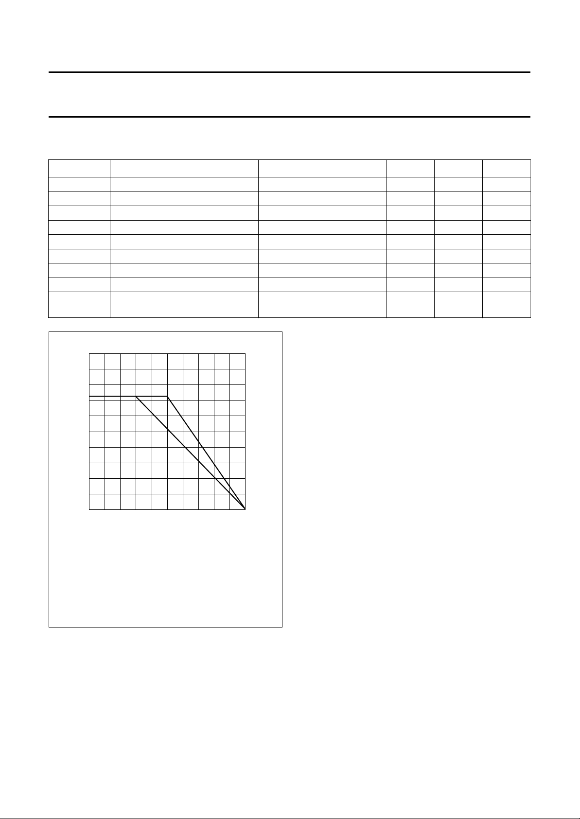
handbook, halfpage
P
tot
(W)
20
15
10
5
0
−50 200
VCE= 24V; f > 1 MHz.
(1) VSWR ≥ 5.
(2) VSWR < 3.
0 50 100 150
(1)
(2)
Fig.2 Power derating curves as functions of
mounting base temperature.
MGD967
Tmb (°C)
1997 Feb 19 3
 Loading...