

Philips PSMN085-150K Datasheet

1. Description
2. Features
PSMN085-150K
N-channel enhancement mode field-effect transistor
Rev. 01 — 16 January 2001 Product specification
SiliconMAX™1 products use the latest Philips TrenchMOS™2 technology to achieve
the lowest possible on-state resistance in a SOT96-1 (SO8) package.
Product availability:
PSMN085-150K in SOT96-1 (SO8).
■ Very low on-state resistance
■ Fast switching
■ TrenchMOS™ technology.
3. Applications
■ DC to DC convertor
■ Computer motherboards
c
c
■ Switch mode power supplies.
4. Pinning information
Table 1: Pinning - SOT96-1, simplified outline and symbol
Pin Description Simplified outline Symbol
1,2,3 source (s)
8
4 gate (g)
5,6,7,8 drain (d)
1
Top view MBK187
SOT96-1 (SO8)
1. SiliconMAX is a trademark of Royal Philips Electronics.
2. TrenchMOS is a trademark of Royal Philips Electronics.
5
4
g
MBB076
d
s

Philips Semiconductors
PSMN085-150K
N-channel enhancement mode field-effect transistor
5. Quick reference data
Table 2: Quick reference data
Symbol Parameter Conditions Typ Max Unit
V
I
P
T
R
DS
D
tot
j
DSon
drain-source voltage (DC) Tj=25to150°C − 150 V
drain current (DC) Tsp=80°C − 4.1 A
total power dissipation Tsp=80°C − 3.5 W
junction temperature − 150 °C
drain-source on-state resistance VGS= 10 V; ID= 3.5 A; Tj=25°C 6785mΩ
6. Limiting values
Table 3: Limiting values
In accordance with the Absolute Maximum Rating System (IEC 60134).
Symbol Parameter Conditions Min Max Unit
V
DS
V
GS
I
D
I
DM
P
tot
T
stg
T
j
Source-drain diode
I
S
I
SM
drain-source voltage (DC) Tj=25to150°C − 150 V
gate-source voltage (DC) −±20 V
drain current (DC) Tsp=80°C; Figure 2 and 3 − 3.5 A
peak drain current Tsp=25°C; pulsed; tp≤ 10 µs; Figure 3 − 40 A
total power dissipation Tsp=80°C; Figure 1 − 3.5 W
storage temperature −55 +150 °C
operating junction temperature −55 +150 °C
source (diode forward) current (DC) Tsp=80°C − 3.1 A
peak source (diode forward) current Tsp=25°C; pulsed; tp≤ 10 µs − 40 A
9397 750 07898
Product specification Rev. 01 — 16 January 2001 2 of 13
© Philips Electronics N.V. 2001. All rights reserved.
Philips Semiconductors
PSMN085-150K
N-channel enhancement mode field-effect transistor
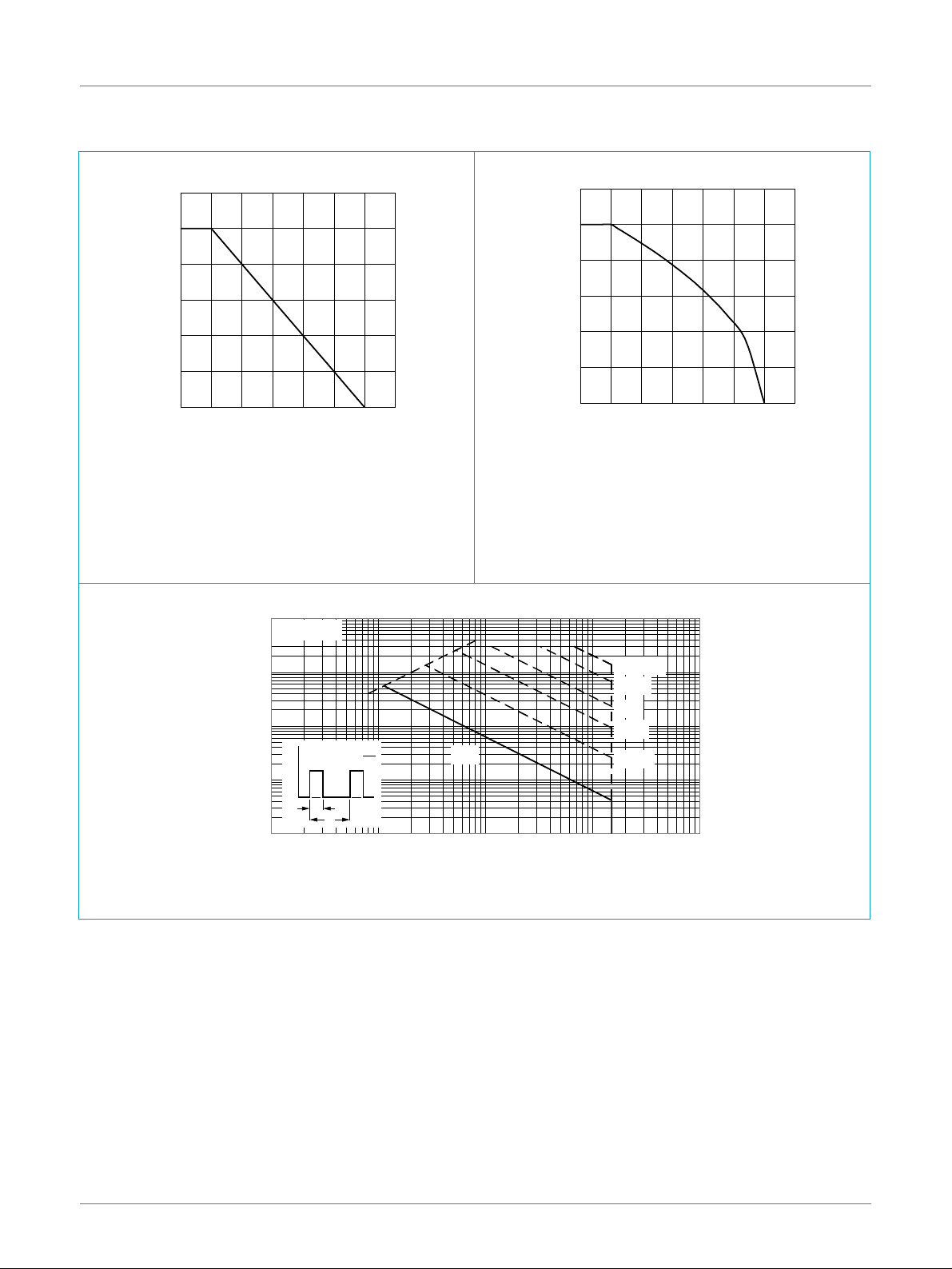
120
P
der
(%)
100
80
60
40
20
0
0 25 50 75 100 125 150 175
P
P
der
tot
----------------------
P
tot 25 C°()
100%×=
03aa17
Tsp (oC)
Fig 1. Normalized total power dissipation as a
function of solder point temperature.
2
10
R
= VDS/ I
10
1
10
10
(A)
DSon
I
D
-1
-2
-1
10
D
t
P
t
p
p
δ =
T
t
T
1 10
120
I
der
(%)
100
80
60
40
20
0
0 25 50 75 100 125 150 175
Tsp (oC)
VGS≥ 5V
I
I
der
D
------------------ -
I
D25C°()
100%×=
Fig 2. Normalized continuous drain current as a
function of solder point temperature.
03ae15
tp = 10 µs
100 µs
1 ms
10 ms
D.C.
10
100 ms
2
VDS (V)
10
3
03aa25
Tsp=25°C; IDM is single pulse
Fig 3. Safe operating area; continuous and peak drain currents as a function of drain-source voltage.
9397 750 07898
Product specification Rev. 01 — 16 January 2001 3 of 13
© Philips Electronics N.V. 2001. All rights reserved.
Philips Semiconductors
PSMN085-150K
N-channel enhancement mode field-effect transistor
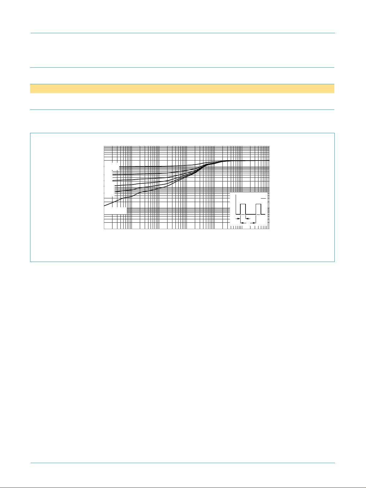
7. Thermal characteristics
Table 4: Thermal characteristics
Symbol Parameter Conditions Value Unit
R
th(j-sp)
thermal resistance from junction to solder
point
7.1 Transient thermal impedance
mounted on a metal clad substrate; Figure 4 20 K/W
10
Z
th(j-sp)
(K/W)
10
1
10
10
2
-1
-2
10
δ = 0.5
0.2
0.1
0.05
0.02
single pulse
-4
P
-3
10
-2
10
-1
10
1 10
03ae14
t
p
δ =
T
t
p
t
T
2
tp (s)
10
Tsp=25°C
Fig 4. Transient thermal impedance from junction to solder point as a function of pulse duration.
9397 750 07898
© Philips Electronics N.V. 2001. All rights reserved.
Product specification Rev. 01 — 16 January 2001 4 of 13
 Loading...