

Philips psmn020 DATASHEETS
Philips Semiconductors Product specification
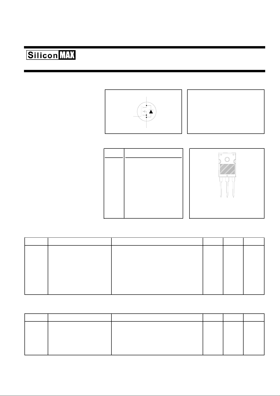
N-channel TrenchMOS transistor PSMN020-150W
FEATURES SYMBOL QUICK REFERENCE DATA
• ’Trench’ technology
• Very low on-state resistance V
d
= 150 V
DSS
• Fast switching
• Low thermal resistance I
g
s
R
DS(ON)
= 73 A
D
≤ 20 mΩ
GENERAL DESCRIPTION PINNING SOT429 (TO247)
SiliconMAXproductsusethelatest PIN DESCRIPTION
Philips Trench technology to
achieve the lowest possible 1 gate
on-state resistance in each
package at each voltage rating. 2 drain
Applications:- 3 source
• d.c. to d.c. converters
2
• switched mode power supplies tab drain
1
The PSMN020-150Wis suppliedin
the SOT429 (TO247) conventional
leaded package.
LIMITING VALUES
Limiting values in accordance with the Absolute Maximum System (IEC 134)
3
SYMBOL PARAMETER CONDITIONS MIN. MAX. UNIT
V
DSS
V
DGR
V
GS
I
D
Drain-source voltage Tj = 25 ˚C to 175˚C - 150 V
Drain-gate voltage Tj = 25 ˚C to 175˚C; RGS = 20 kΩ - 150 V
Gate-source voltage - ± 20 V
Continuous drain current Tmb = 25 ˚C - 73 A
Tmb = 100 ˚C - 51 A
I
DM
P
D
Tj, T
Pulsed drain current Tmb = 25 ˚C - 290 A
Total power dissipation Tmb = 25 ˚C - 300 W
Operating junction and - 55 175 ˚C
stg
storage temperature
AVALANCHE ENERGY LIMITING VALUES
Limiting values in accordance with the Absolute Maximum System (IEC 134)
SYMBOL PARAMETER CONDITIONS MIN. MAX. UNIT
E
AS
I
AS
Non-repetitive avalanche Unclamped inductive load, IAS = 73 A; - 707 mJ
energy tp = 100 µs; Tj prior to avalanche = 25˚C;
VDD ≤ 25 V; RGS = 50 Ω; VGS = 5 V; refer to
fig:15
Non-repetitive avalanche - 73 A
current
November 1999 1 Rev 1.000

Philips Semiconductors Product specification
N-channel TrenchMOS transistor PSMN020-150W
THERMAL RESISTANCES
SYMBOL PARAMETER CONDITIONS TYP. MAX. UNIT
R
th j-mb
R
th j-a
ELECTRICAL CHARACTERISTICS
Tj= 25˚C unless otherwise specified
SYMBOL PARAMETER CONDITIONS MIN. TYP. MAX. UNIT
V
(BR)DSS
V
GS(TO)
R
DS(ON)
I
GSS
I
DSS
Q
g(tot)
Q
gs
Q
gd
t
d on
t
r
t
d off
t
f
L
d
L
d
L
s
C
iss
C
oss
C
rss
Thermal resistance junction - 0.5 K/W
to mounting base
Thermal resistance junction in free air 45 - K/W
to ambient
Drain-source breakdown VGS = 0 V; ID = 0.25 mA; 150 - - V
voltage Tj = -55˚C 134 - - V
Gate threshold voltage VDS = VGS; ID = 1 mA 2.0 3.0 4.0 V
Tj = 175˚C 1.0 - - V
Tj = -55˚C - - 6 V
Drain-source on-state VGS = 10 V; ID = 25 A - 12 20 mΩ
resistance Tj = 175˚C - - 56 mΩ
Gate source leakage current VGS = ±10 V; VDS = 0 V - 2 100 nA
Zero gate voltage drain VDS = 150 V; VGS = 0 V; - 0.05 10 µA
current Tj = 175˚C - - 500 µA
Total gate charge ID = 73 A; V
= 120 V; VGS = 10 V - 227 - nC
DD
Gate-source charge - 46 - nC
Gate-drain (Miller) charge - 91 - nC
Turn-on delay time VDD = 75 V; RD = 2.7 Ω; - 34 - ns
Turn-on rise time VGS = 10 V; RG = 5.6 Ω -79-ns
Turn-off delay time Resistive load - 233 - ns
Turn-off fall time - 101 - ns
Internal drain inductance Measured from tab to centre of die - 3.5 - nH
Internal drain inductance Measured from drain lead to centre of die - 4.5 - nH
Internal source inductance Measured from source lead to source - 7.5 - nH
bond pad
Input capacitance VGS = 0 V; VDS = 25 V; f = 1 MHz - 9537 - pF
Output capacitance - 854 - pF
Feedback capacitance - 380 - pF
REVERSE DIODE LIMITING VALUES AND CHARACTERISTICS
Tj = 25˚C unless otherwise specified
SYMBOL PARAMETER CONDITIONS MIN. TYP. MAX. UNIT
I
S
I
SM
V
SD
t
rr
Q
rr
November 1999 2 Rev 1.000
Continuous source current - - 73 A
(body diode)
Pulsed source current (body - - 290 A
diode)
Diode forward voltage IF = 25 A; VGS = 0 V - 0.85 1.2 V
IF = 75 A; VGS = 0 V - 1.1 - V
Reverse recovery time IF = 20 A; -dIF/dt = 100 A/µs; - 127 - ns
Reverse recovery charge VGS = 0 V; VR = 30 V - 1.0 - µC
Philips Semiconductors Product specification
N-channel TrenchMOS transistor PSMN020-150W
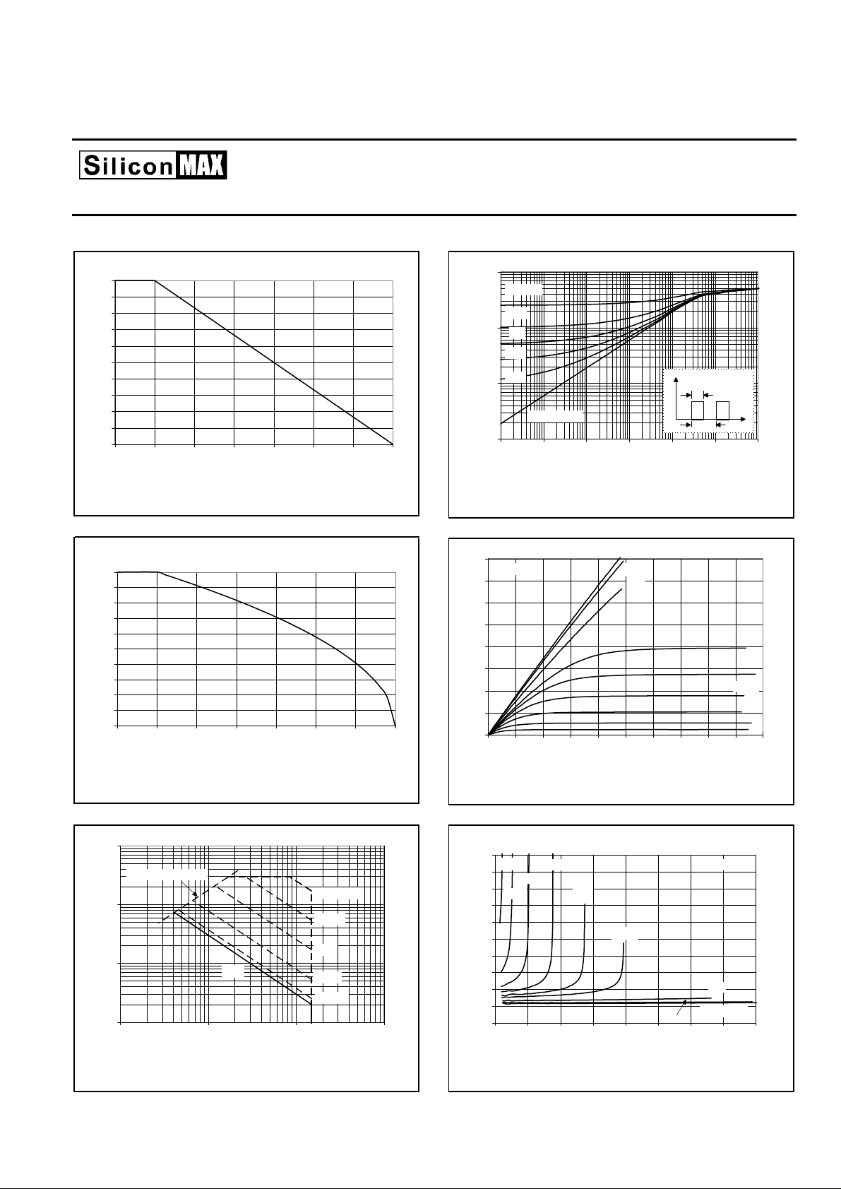
Normalised Power Derating, PD (%)
100
90
80
70
60
50
40
30
20
10
0
0 25 50 75 100 125 150 175
Mounting Base temperature, Tmb (C)
Fig.1. Normalised power dissipation.
PD% = 100⋅PD/P
Normalised Current Derating, ID (%)
100
90
80
70
60
50
40
30
20
10
0
0 25 50 75 100 125 150 175
Mounting Base temperature, Tmb (C)
D 25 ˚C
= f(Tmb)
Fig.2. Normalised continuous drain current.
ID% = 100⋅ID/I
= f(Tmb); VGS ≥ 10 V
D 25 ˚C
Transient thermal impedance, Zth j-mb (K/W)
1
D = 0.5
0.2
0.1
0.1
0.05
0.02
0.01
single pulse
0.001
1E-06 1E-05 1E-04 1E-03 1E-02 1E-01 1E+00
Pulse width, tp (s)
P
D
tp
D = tp/T
T
Fig.4. Transient thermal impedance.
Z
= f(t); parameter D = tp/T
th j-mb
Drain Current, ID (A)
80
Tj = 25 C VGS = 10V
70
60
50
40
30
20
10
0
0 0.2 0.4 0.6 0.8 1 1.2 1.4 1.6 1.8 2
Drain-Source Voltage, VDS (V)
8 V
6 V
4.2 V
5.2 V
5 V
4.8 V
4.6 V
4.4 V
Fig.5. Typical output characteristics, Tj = 25 ˚C
ID = f(VDS)
.
Peak Pulsed Drain Current, IDM (A)
1000
RDS(on) = VDS/ ID
100
10
1
1 10 100 1000
D.C.
Drain-Source Voltage, VDS (V)
tp = 10 us
100 us
1 ms
10 ms
100 ms
Fig.3. Safe operating area
ID & IDM = f(VDS); IDM single pulse; parameter t
p
Drain-Source On Resistance, RDS(on) (Ohms)
0.1
4.2 V
0.09
0.08
0.07
0.06
0.05
0.04
0.03
0.02
0.01
0
0 1020304050607080
4.4V
4.6 V
4.8 V
5V
Drain Current, ID (A)
5.2V
8 V
Tj = 25 C
6 V
VGS = 10V
Fig.6. Typical on-state resistance, Tj = 25 ˚C
R
= f(ID)
DS(ON)
.
November 1999 3 Rev 1.000
 Loading...