

Philips PSMN005-25D Datasheet

DISCRETE SEMICONDUCTORS
DATA SH EET
PSMN005-25D
N-channel logic level
TrenchMOS
Product specification October 1999
(TM)
transistor
Philips Semiconductors Product specification
N-channel logic level TrenchMOS
(TM)
transistor
PSMN005-25D
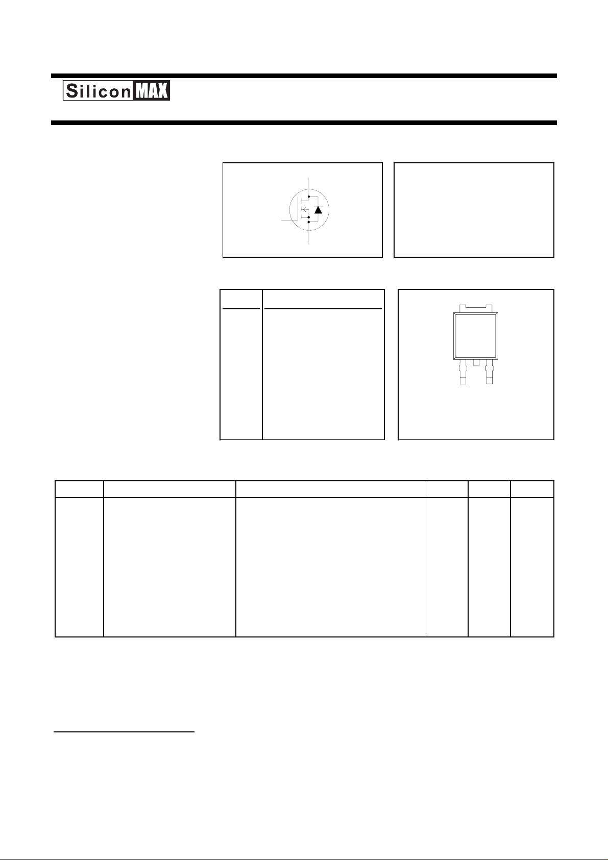
FEATURES SYMBOL QUICK REFERENCE DATA
• ’Trench’ technology V
• Very low on-state resistance
• Fast switching
• Logic level compatible
g
d
= 25 V
DSS
ID = 75 A
R
s
≤ 5.8 mΩ (VGS = 10 V)
DS(ON)
R
≤ 7.5 mΩ (VGS = 5 V)
DS(ON)
GENERAL DESCRIPTION PINNING SOT428 (DPAK)
SiliconMAXproductsusethelatest PIN DESCRIPTION
Philips Trench technology to
achieve the lowest possible 1 gate
on-state resistance in each
package at each voltage rating. 2 drain
1
Applications:- 3 source
• d.c. to d.c. converters
• switched mode power supplies tab drain
tab
2
1
3
The PSMN005-25D is supplied in
the SOT428 (Dpak) surface
mounting package.
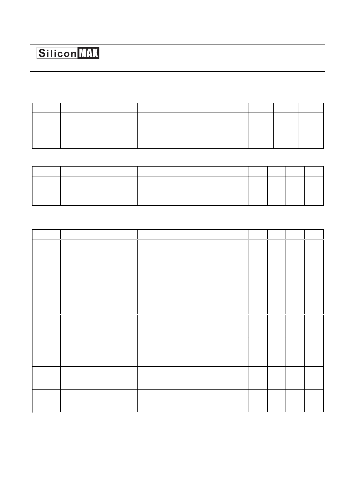
LIMITING VALUES
Limiting values in accordance with the Absolute Maximum System (IEC 134)
SYMBOL PARAMETER CONDITIONS MIN. MAX. UNIT
V
DSS
V
DGR
V
GS
V
GSM
I
D
I
DM
P
D
T
, T
j
Drain-source voltage Tj = 25 ˚C to 175˚C - 25 V
Drain-gate voltage Tj = 25 ˚C to 175˚C; RGS = 20 kΩ -25V
Continuous gate-source - ± 15 V
voltage
Peak pulsed gate-source Tj ≤ 150 ˚C - ± 20 V
voltage
Continuous drain current Tmb = 25 ˚C; VGS = 5 V - 75
T
= 100 ˚C; VGS = 5 V - 70 A
mb
2
Pulsed drain current Tmb = 25 ˚C - 240 A
Total power dissipation Tmb = 25 ˚C - 125 W
Operating junction and - 55 175 ˚C
stg
storage temperature
A
1 It is not possible to make connection to pin 2 of the SOT428 package.
2 Continuous current rating limited by package.
October 1999 2 Rev 1.100
Philips Semiconductors Product specification
(TM)
transistor
PSMN005-25DN-channel logic level TrenchMOS
AVALANCHE ENERGY LIMITING VALUES
Limiting values in accordance with the Absolute Maximum System (IEC 134)
SYMBOL PARAMETER CONDITIONS MIN. MAX. UNIT
E
AS
I
AS
Non-repetitive avalanche Unclamped inductive load, IAS = 75 A; - 120 mJ
energy t
= 100 µs; Tj prior to avalanche = 25˚C;
p
V
≤ 15 V; RGS = 50 Ω; VGS = 5 V
DD
Non-repetitive avalanche - 75 A
current
THERMAL RESISTANCES
SYMBOL PARAMETER CONDITIONS MIN. TYP. MAX. UNIT
R
th j-mb
Thermal resistance junction - - 1.2 K/W
to mounting base
R
th j-a
Thermal resistance junction SOT428 package, pcb mounted, minimum - 50 - K/W
to ambient footprint
ELECTRICAL CHARACTERISTICS
Tj= 25˚C unless otherwise specified
SYMBOL PARAMETER CONDITIONS MIN. TYP. MAX. UNIT
V
(BR)DSS
V
GS(TO)
R
DS(ON)
I
GSS
I
DSS
Q
g(tot)
Q
gs
Q
gd
t
d on
t
r
t
d off
t
f
L
d
L
s
C
iss
C
oss
C
rss
Drain-source breakdown VGS = 0 V; ID = 0.25 mA; 25 - - V
voltage T
= -55˚C 23 - - V
j
Gate threshold voltage VDS = VGS; ID = 1 mA 1 1.5 2 V
T
= 175˚C 0.5 - - V
j
= -55˚C - - 2.3 V
T
j
Drain-source on-state VGS = 10 V; ID = 25 A - 5 5.8 mΩ
resistance V
= 5 V; ID = 25 A - 6.2 7.5 mΩ
GS
V
= 5 V; ID = 25 A; Tj = 175˚C - - 14 mΩ
GS
Gate source leakage current VGS = ±10 V; VDS = 0 V - 0.02 100 nA
Zero gate voltage drain VDS = 25 V; VGS = 0 V; - 0.05 10 µA
current T
Total gate charge ID = 75 A; V
= 15 V; VGS = 5 V - 60 - nC
DD
= 175˚C - - 500 µA
j
Gate-source charge - 8 - nC
Gate-drain (Miller) charge - 32 - nC
Turn-on delay time VDD = 15 V; RD = 0.6 Ω; - 21 - ns
Turn-on rise time VGS = 10 V; RG = 10 Ω - 170 - ns
Turn-off delay time Resistive load - 270 - ns
Turn-off fall time - 216 - ns
Internal drain inductance Measured tab to centre of die - 3.5 - nH
Internal source inductance Measured from source lead to source - 7.5 - nH
bond pad
Input capacitance VGS = 0 V; VDS = 20 V; f = 1 MHz - 3500 - pF
Output capacitance - 970 - pF
Feedback capacitance - 640 - pF
October 1999 3 Rev 1.100
Philips Semiconductors Product specification
(TM)
transistor
PSMN005-25DN-channel logic level TrenchMOS
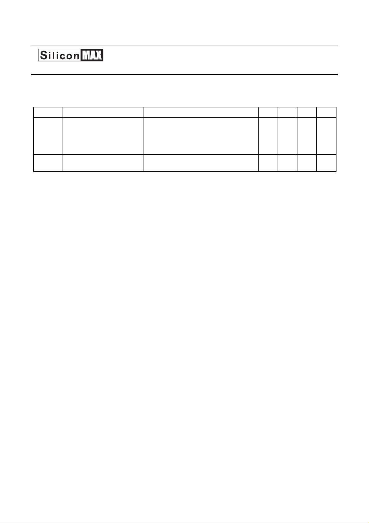
REVERSE DIODE LIMITING VALUES AND CHARACTERISTICS
Tj = 25˚C unless otherwise specified
SYMBOL PARAMETER CONDITIONS MIN. TYP. MAX. UNIT
I
S
I
SM
V
SD
t
rr
Q
rr
Continuous source current - - 75 A
(body diode)
Pulsed source current (body - - 240 A
diode)
Diode forward voltage IF = 25 A; VGS = 0 V - 0.95 1.2 V
Reverse recovery time IF = 25 A; -dIF/dt = 100 A/µs; - 140 - ns
Reverse recovery charge VGS = 0 V; VR = 25 V - 0.27 - µC
October 1999 4 Rev 1.100
 Loading...