

Philips PSMN004-36P, PSMN004-36B User Manual

查询PSMN004-36B供应商
1. Description
N-channel logic level field-effect power transistor in a plastic package using
TrenchMOS™1 technology.
Product availability:
2. Features
PSMN004-36P/36B
N-channel enhancement mode field-effect transistor
Rev. 01 — 19 November 2001 Product data
PSMN004-36P in SOT78 (TO-220AB)
PSMN004-36B in SOT404 (D2-PAK).
■ Very low on-state resistance
■ Fast switching.
3. Applications
■ DC to DC converters
■ Switch mode power supplies.
4. Pinning information
Table 1: Pinning - SOT78 and SOT404, simplified outline and symbol
Pin Description Simplified outline Symbol
1 gate (g)
2 drain (d)
3 source (s)
mb drain (d)
[1]
MBK106
12mb3
SOT78 (TO-220AB) SOT404 (D
mb
2
13
2-
PAK)
MBK116
g
MBB076
d
s
[1] It is not possible to make connection to pin 2 of the SOT404 package.
1. TrenchMOS is a trademark of Koninklijke Philips Electronics N.V.

Philips Semiconductors
PSMN004-36P/36B
N-channel enhancement mode field-effect transistor
5. Quick reference data
Table 2: Quick reference data
Symbol Parameter Conditions Typ Max Unit
V
I
D
P
T
R
DS
tot
j
DSon
drain-source voltage (DC) Tj=25to175°C − 36 V
drain current (DC) Tmb=25°C; VGS=5V − 75 A
total power dissipation Tmb=25°C − 230 W
junction temperature − 175 °C
drain-source on-state resistance VGS= 10 V; ID= 25 A; Tj= 25°C 3.5 4 mΩ
=5V; ID= 25 A; Tj= 25°C 45mΩ
V
GS
6. Limiting values
Table 3: Limiting values
In accordance with the Absolute Maximum Rating System (IEC 60134).
Symbol Parameter Conditions Min Max Unit
V
DS
V
DGR
V
GS
V
GSM
I
D
I
DM
P
tot
T
stg
T
j
Source-drain diode
I
S
I
SM
Avalanche ruggedness
E
AS
I
AS
drain-source voltage (DC) Tj=25to175°C − 36 V
drain-gate voltage (DC) Tj=25to175°C; RGS=20kΩ−36 V
gate-source voltage (DC) −±15 V
gate-source voltage tp≤ 50 µs; pulsed;
duty cycle 25 %; T
≤ 150 °C
j
−±20 V
drain current (DC) Tmb=25°C; VGS=5V;Figure 2 and 3 − 75 A
= 100 °C; VGS=5V;Figure 2 − 75 A
T
mb
peak drain current Tmb=25°C; pulsed; tp≤ 10 µs; Figure 3 − 240 A
total power dissipation Tmb=25°C; Figure 1 − 230 W
storage temperature −55 +175 °C
operating junction temperature −55 +175 °C
source (diode forward) current (DC) Tmb=25°C − 75 A
peak source (diode forward) current Tmb=25°C; pulsed; tp≤ 10 µs − 240 A
non-repetitive avalanche energy unclamped inductive load;
=75A;tp= 0.1 ms; VDD=15V;
I
D
=50Ω; VGS= 5V; starting Tj=25°C;
R
GS
non-repetitive avalanche current unclamped inductive load;
=15V;RGS=50Ω; VGS=5V;
V
DD
starting T
=25°C
j
− 120 mJ
− 75 A
9397 750 08621
Product data Rev. 01 — 19 November 2001 2 of 13
© Koninklijke Philips Electronics N.V. 2001. All rights reserved.
Philips Semiconductors
PSMN004-36P/36B
N-channel enhancement mode field-effect transistor
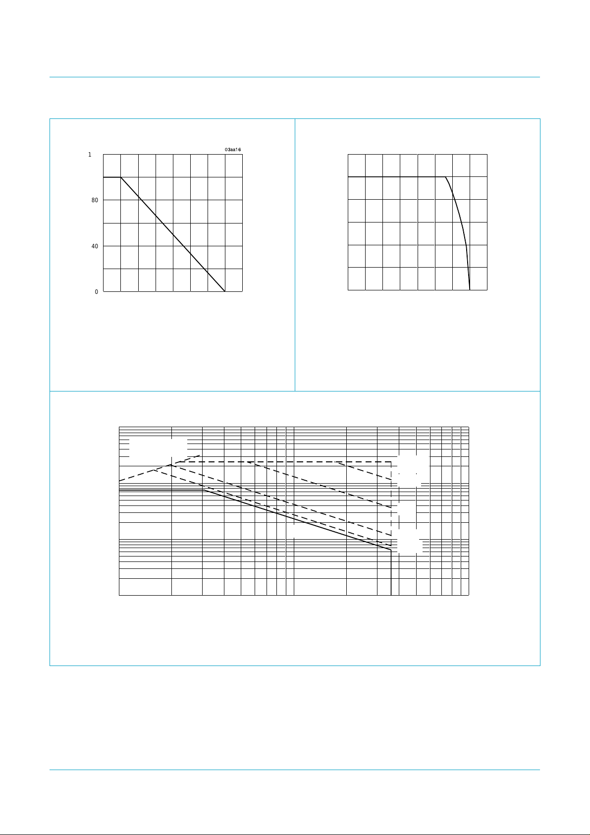
120
P
der
(%)
80
40
0
0 50 100 150 200
P
tot
P
der
-----------------------
P
tot 25 C°()
100%×= I
03aa16
T
(oC)
mb
Fig 1. Normalized total power dissipation as a
function of mounting base temperature.
3
10
120
I
D
(%)
80
40
0
0 50 100 150 200
I
D
der
-------------------
I
D25C
()
100%×=
°
03ag42
Tmb (ºC)
Fig 2. Normalized continuous drain current as a
function of mounting base temperature.
03ag44
R
I
D
(A)
2
10
10
1
1 10 10
DS(on)
= VDS/ I
D
tp = 10 us
100 us
1 ms
DC
10 ms
100 ms
2
(V)
V
DS
Tmb=25°C; IDM is single pulse.
Fig 3. Safe operating area; continuous and peak drain currents as a function of drain-source voltage.
9397 750 08621
© Koninklijke Philips Electronics N.V. 2001. All rights reserved.
Product data Rev. 01 — 19 November 2001 3 of 13
Philips Semiconductors
PSMN004-36P/36B
N-channel enhancement mode field-effect transistor
7. Thermal characteristics
Table 4: Thermal characteristics
Symbol Parameter Conditions Value Unit
R
th(j-mb)
R
th(j-a)
thermal resistance from junction to mounting
base
thermal resistance from junction to ambient vertical in still air; SOT78 package 60 K/W
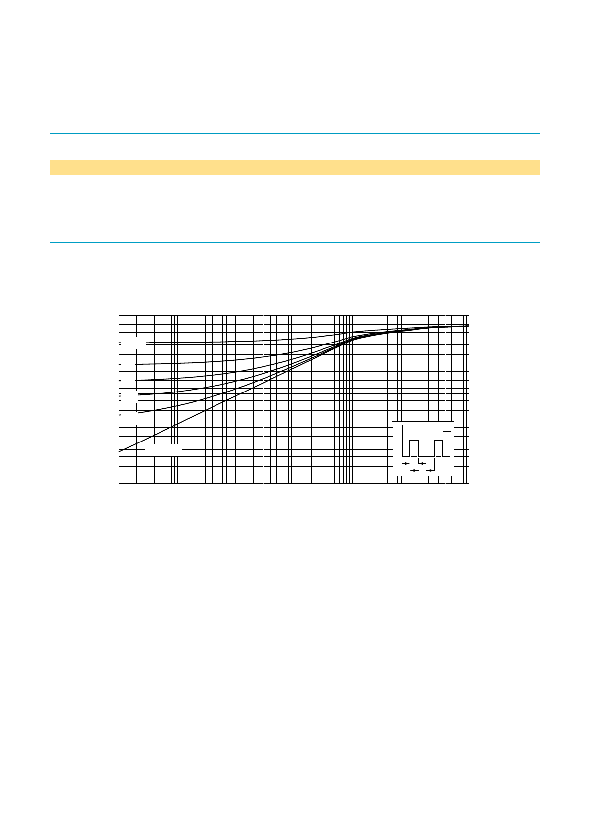
7.1 Transient thermal impedance
Figure 4 0.65 K/W
mounted on a printed circuit board;
50 K/W
minimum footprint; SOT404 package
03ag43
t
p
δ =
T
t
1
(s)
t
p
Z
th j-mb
(K/W)
1
10
10
10
δ = 0.5
0.2
-1
0.1
0.05
0.02
-2
single pulse
-3
10
-6
10
-5
10
-4
10
-3
10
-2
P
t
p
T
-1
10
Fig 4. Transient thermal impedance from junction to mounting base as a function of pulse duration.
9397 750 08621
© Koninklijke Philips Electronics N.V. 2001. All rights reserved.
Product data Rev. 01 — 19 November 2001 4 of 13
 Loading...