

Philips PR31700 Datasheet

INTEGRATED CIRCUITS
PR31700
32-bit RISC microprocessor
Preliminary specification
Supersedes data of 1997 Dec 15
1998 May 13

Philips Semiconductors Preliminary specification
PR3170032-bit RISC microprocessor
GENERAL DESCRIPTION
The PR31700 is a single-chip digital ASSP (Application Specific
Stand Product) used in HPCs (Handheld Personal Computers),
Palm-size PCs, Screenphones, Smartphones, and other vertical
market applications in the mobile computing and communication
markets. The PR31700 consists of system support logic, integrated
with the PR3901 Processor Core designed by Philips
Semiconductors.
FEATURES
• R3000A-based PR3901 Processor Core
– RISC architecture developed by MIPS Technologies, Inc.
– Philips has added its own multiply-add and branch-likely
instructions.
– A single-cycle multiply/accumulate module to allow integrated
DSP functions, such as a software modem for
high-performance standard data and fax protocols
– Instruction cache: 4K bytes; data cache: 1K bytes
– On-chip Translation Lookaside Buffer (TLB) with 3264-bit wide
entries, each of which maps 4KByte page Max 75MHz
operation
• Built-in peripheral circuit
– Clock generator with built-in eightfold-frequency phase-locked
loop (PLL)
– Four-stage write buffer
– A high performance and flexible Bus Interface Unit
– Multiple DMA channels
– Memory controller for DRAM, HDRAM, SDRAM, SRAM, ROM,
Flash Memory and PCMCIA
– Power management unit
– Big / Little endian
• Low power dissipation
– 3.3V operation
– Standby Current 10A(typ)
– CPU clock stop mode
– Power down modes for individual internal peripheral modules
• Plastic LQFP 208-pin package
The information contained herein is subject to change without notice.
Philips is continually working to improve the quality and the reliability of its products. Nevertheless, semiconductor devices in general
can malfunction or fail due to their inherent electrical sensitivity and vulnerability to physical stress. It is the responsibility of the
buyer, when utilizing Philips products, to observe standards of safety, and to avoid situations in which a malfunction or failure of
a Philips product could cause loss of human life, bodily injury or damage to property.
In developing your designs, please ensure that Philips products are used within specified operating ranges as set forth in the
most recent products specifications. Also, please keep in mind the precautions and conditions set forth in the Philips
Semiconductor Reliability Handbook
The information contained herein is presented only as a guide for the applications of our products. No responsibility is assumed by Philips for
any infringements of patents or other rights of the third parties which may result from its use. No license is granted by implication or
otherwise under any patent or patent rights of Philips or others.
R3000A is a trademark of MIPS Technologies, Inc.
1998 May 13
2
Philips Semiconductors Preliminary specification
PR3170032-bit RISC microprocessor
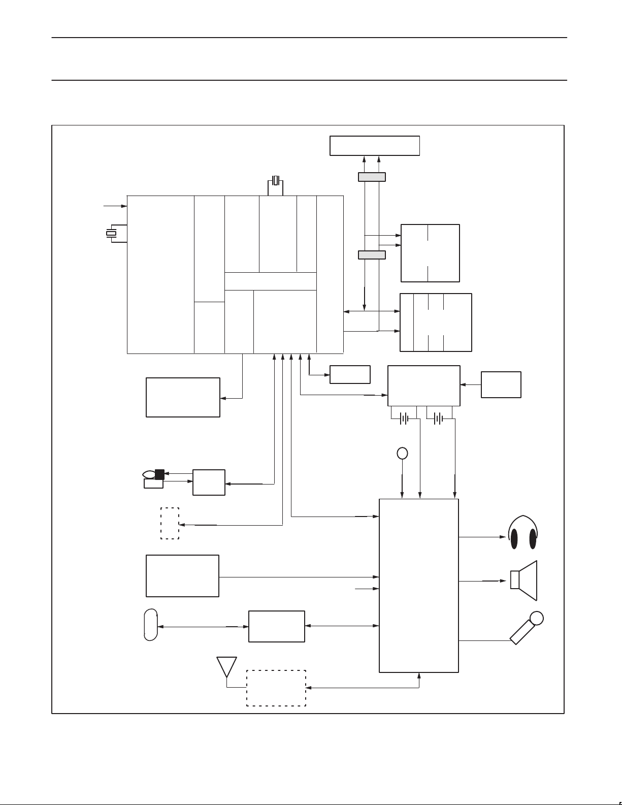
SYSTEM CONFIGURATION
1–2 PCMCIA SLOTS
32KHZ
3.3V
SYSCLK
PR31700
(208–PIN PQFP)
PR3901
RISC
CPU
CORE
LCD
RAM
RAM
IR
I–CACHE/
INTERFACE
I–CACHE/
TLB
32–BIT BUS
LCD
REAL–TIME CLOCK
PCMCIA/ROM/I/F
TIMERS
SERIAL I/F
DRAM/SDRAM INTERFACE
ID ROM
THERMISTOR
MAIN
T
1–64
MBYTES
ROM
1–32
MBYTES(S)
DRAM
POWER
SUPPLY
ADAPTER
BACKUP
(LITHIUM)
AC
1998 May 13
ISDN OR OTHER
PERIPHERALS
PHONE
JACK
TOUCHSCREEN
(RESISTIVE)
HIGH SPEED
SERIAL PORT
DAA
OR
DAA
Figure 1. System Block Diagram
3
3.3V
BETTY
UCB1200
(ANALOG ASIC)
44–PIN QFP
SN00183
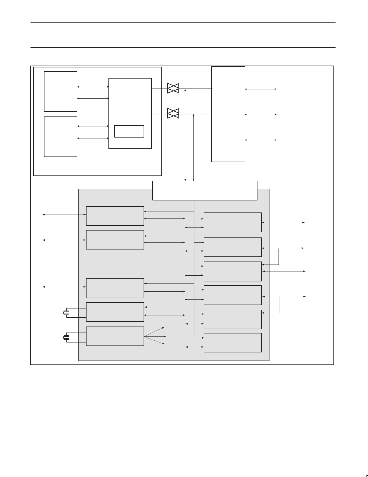
Philips Semiconductors Preliminary specification
PR3170032-bit RISC microprocessor
ICACHE
4 KBYTE
DCACHE
1 KBYTE
TO BETTY
TO LCD
DATA
ADDR
DATA
ADDR
R3901
PROCESSOR CORE
SIB MODULE
VIDEO MODULE
PR3901
RISC CUP
CORE
MAC
DATA
ADDR
SYSTEM INTERFACE UNIT (SIU) MODULE ARBITRATION/
DMA/ADR DECODE
DATA ADDR
BUS INTERFACE UNIT (BIU) MODULE
(S) DRAM/PCMCIA/ROM
CHI MODULE
IR MODULE
DATA
ADDR
CONTROL
TO
MEMORY
TO HIGH
SPEED SERIAL
TO IR
TO GENERAL
PURPOSE I/O
32 KHZ
SYSCLK
IO MODULE
TIMER MODULE
(+ RTC)
CLOCK MODULE
SYSTEM INTERFACE MODULE (SIM)
Figure 2. PR31700 Block Diagram
UART MODULE
(DUAL UART)
SPI MODULE
POWER MODULE
INTERRUPT MODULE
TO UART
TO POWER
SUPPLY
SN00184
1998 May 13
4
Philips Semiconductors Preliminary specification
PR3170032-bit RISC microprocessor
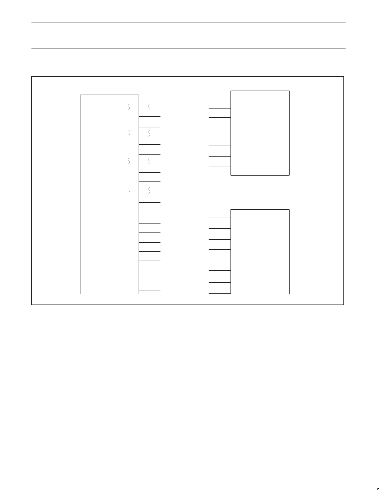
MEMORY CONNECTIONS
PR31700
D[31]
D[24]
D[23]
D[16]
D[15]
D[8]
D[7]
D[0]
CAS3*
CAS2*
CAS1*
CAS0*
RAS0*
WE*
A[12:0]
PIN NO.
133 D[31]
145 D[24]
146 D[23]
159 D[16]
27D[16]
16 D[8]
14 D[7]
2 D[0]
195 CAS3*
197 CAS2*
198 CAS1*
199 CAS0*
194 RAS0*
169 WE*
A[12:0]
CAS1*
CAS0*
RASO*
WE*
A(12:0)
CAS3*
CAS2*
CAS1*
CAS0*
RAS0*
WE*
A(12:0)
CASHI*
CASLO*
RAS*
WE*
ADDR
CAS HI*
CAS MH*
CAS ML*
CAS LO*
RAS*
WE*
ADDR
BANK0
16BIT
DRAM
D(15:0)DATA
BANK1
32BIT
D(31:0)DATA
1998 May 13
BIG ENDIAN
Figure 3. Memory Connections
5
SN00185
Philips Semiconductors Preliminary specification
PR3170032-bit RISC microprocessor
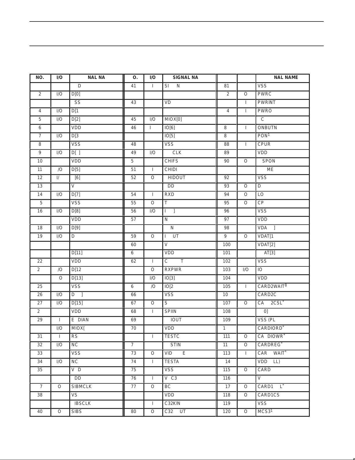
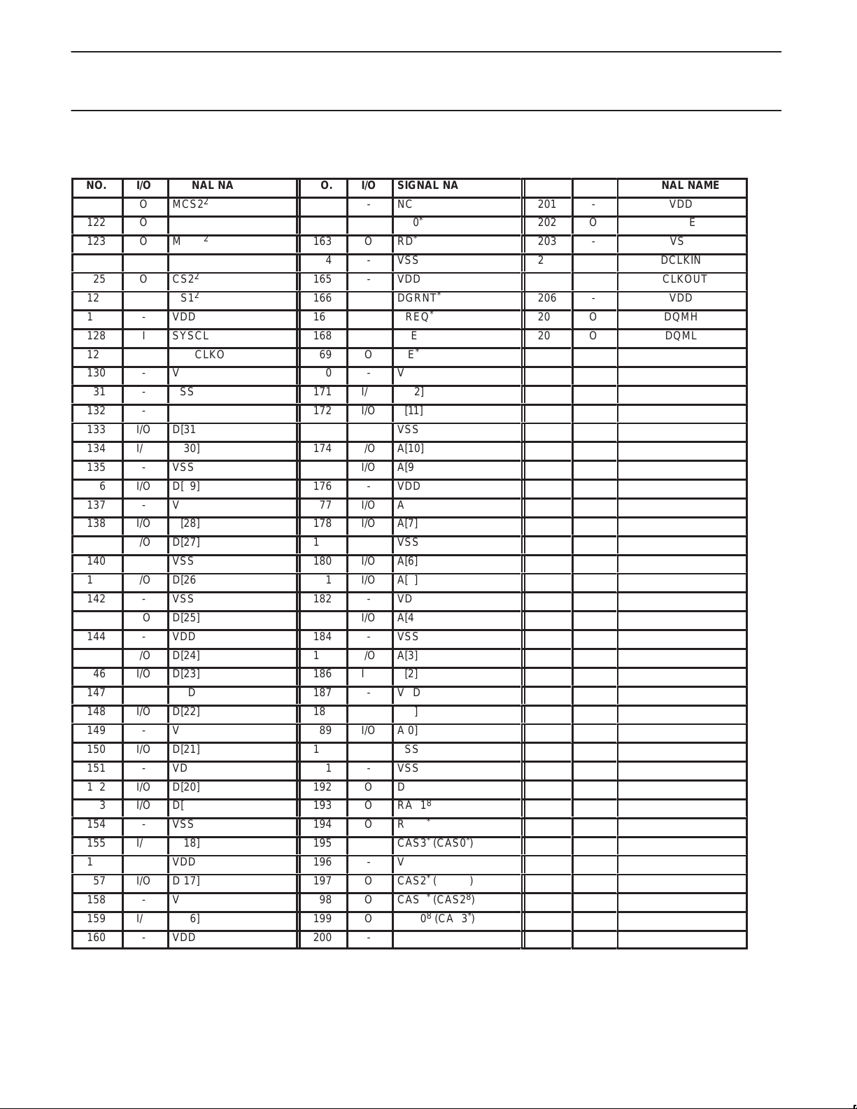
PIN ASSIGNMENTS
NO.
1
2
3
4
5
6
7
8
9
10
11
12
13
14
15
16
17
18
19
20
21
22
23
24
25
26
27
28
29
30
31
32
33
34
35
36
37
38
39
40
I/O
I/O
I/O
I/O
I/O
I/O
I/O
I/O
I/O
I/O
I/O
I/O
I/O
I/O
I/O
I/O
I/O
I/O
I/O
I/O
O
O
O
I
I
SIGNAL NAME
VDD
D[0]
VSS
D[1]
D[2]
VDD
D[3]
VSS
D[4]
VDD
D[5]
D[6]
VSS
D[7]
VSS
D[8]
VDD
D[9]
D[10]
VSS
D[11]
VDD
D[12]
D[13]
VSS
D[14]
D[15]
VDD
ENDIAN
MIOX[1]
RSRV1
NC
VSS
NC
VDD
VDD
SIBMCLK
VSS
SIBSCLK
SIBSYNC
NO.
41
42
43
44
45
46
47
48
49
50
51
52
53
54
55
56
57
58
59
60
61
62
63
64
65
66
67
68
69
70
71
72
73
74
75
76
77
78
79
80
I/O
O
I/O
I/O
I/O
I/O
I/O
O
O
I/O
O
O
I/O
I/O
O
O
O
O
O
I
I
I
I
I
I
I
I
I
I
I
I
SIGNAL NAME
SIBDIN
SIBDOUT
VDD
SIBIRQ
MIOX[0]
IO[6]
IO[5]
VSS
CHICLK
CHIFS
CHIDIN
CHIDOUT
VDD
RXD
TXD
IO[4]
NC
IRIN
IROUT
VSS
VDD
CARDET
RXPWR
IO[3]
IO[2]
VSS
SPICLK
SPIIN
SPIOUT
VDD
TESTCPU
TESTIN
VIDDONE
TESTAIU
VSS
VCC3
BC32K
VDD
C32KlN
C32KOUT
NO.
81
82
83
84
85
86
87
88
89
90
91
92
93
94
95
96
97
98
99
100
101
102
103
104
105
106
107
108
109
110
111
112
113
114
115
116
117
118
119
120
I/O
O
I
I
I
I
I
O
O
O
O
O
O
O
O
O
I/O
I
O
O
I/O
O
O
O
I
O
O
O
O
SIGNAL NAME
VSS
PWRCS
PWRlNT
PWROK
NC
ONBUTN
1
PON
CPURES
*
VDD
DISPON
FRAME
VSS
DF
LOAD
CP
VSS
VDD
VDAT[0]
VDAT[1]
VDAT[2]
VDAT[3]
VSS
IO[1]
VDD
CARD2WAIT
CARD2CSH
CARD2CSL
IO[0]
VSS (PLL)
CARDIORD
CARDIOWR
CARDREG
CARD1WAIT
VDD (PLL)
CARDDIR
*
VDD
CARD1CSL
CARD1CSH
VSS
1
MCS3
8
*
*
*
*
*
*
*
*
1998 May 13
6
Philips Semiconductors Preliminary specification
PR3170032-bit RISC microprocessor
PIN ASSIGNMENTS (Continued)
NO.
121
122
123
124
125
126
127
128
129
130
131
132
133
134
135
136
137
138
139
140
141
142
143
144
145
146
147
148
149
150
151
152
153
154
155
156
157
158
159
160
I/O
O
O
O
O
O
O
I
O
-
-
I/O
I/O
I/O
I/O
I/O
I/O
I/O
I/O
I/O
I/O
I/O
I/O
I/O
I/O
I/O
I/O
-
SIGNAL NAME
2
MCS2
2
MCS1
2
MCS0
2
CS3
2
CS2
2
CS1
VDD
SYSCLKIN
SYSCLKOUT
VSS
VSS
VDD
D[31]
D[30]
VSS
D[29]
VDD
D[28]
D[27]
VSS
D[26]
VSS
D[25]
VDD
D[24]
D[23]
VDD
D[22]
VSS
D[21]
VDD
D[20]
D[19]
VSS
D[18]
VDD
D[17]
VSS
D[16]
VDD
NO.
161
162
163
164
165
166
167
168
169
170
171
172
173
174
175
176
177
178
179
180
181
182
183
184
185
186
187
188
189
190
191
192
193
194
195
196
197
198
199
200
I/O
O
O
-
O
I
O
O
I/O
I/O
I/O
I/O
I/O
I/O
I/O
I/O
I/O
I/O
I/O
I/O
I/O
-
-
O
O
O
O
-
O
O
O
-
SIGNAL NAME
NC
*
CS0
*
RD
VSS
VDD
*
DGRNT
*
DREQ
ALE
*
WE
VDD
A[12]
A[11]
VSS
A[10]
A[9]
VDD
A[8]
A[7]
VSS
A[6]
A[5]
VDD
A[4]
VSS
A[3]
A[2]
VDD
A[1]
A[0]
VSS
VSS
*
DCS0
8
RAS1
*
RAS0
CAS3* (CAS0*)
VDD
CAS2* (CAS1*)
CAS1* (CAS28)
CAS08 (CAS3*)
VSS
NO.
201
202
203
204
205
206
207
208
I/O
SIGNAL NAME
-
O
I
O
O
O
VDD
DCKE
VSS
DCLKIN
DCLKOUT
VDD
DQMH
DQML
1998 May 13
7
Philips Semiconductors Preliminary specification
PR3170032-bit RISC microprocessor
PIN FUNCTIONS
NAME I/O FUNCTIONS
Memory Pins
D(31:0) I/O These pins are the data bus for the system. 8-bit SDRAMs should be connected to bits 7:0 and 16-bit
A(12:0) O These pins are the address bus for the system. The address lines are multiplexed and can be connected
ALE O This pin is used as the address latch enable to latch A(12:0) using an external latch, for generating the
*
RD
O This pin is used as the read signal for static devices. This signal is asserted for reads from /MCS3*-0*,
WE* O This pin is used as the write signal for the system. This signal is asserted for writes to /MCS3*-0*, /CS3*-0*,
CAS0* (/WE0)
CAS* (/WE1)
CAS2* (/WE2)
CAS3* (/WE3)
RAS0
RAS1* (/DCS1)
DCS0
*
*
*
*
*
*
*
O This pin is used as the CAS signal for SDRAMs, the CAS signal for D(7:0) for DRAMs, and the write enable
O This pin is used as the CAS signal for D(15:8) for DRAMs and the write enable signal for D(15:8) for static
O This pin is used as the CAS signal for D(23:16) for DRAMs and the write enable signal for D(23:16) for
O This pin is used as the CAS signal for D(31:24) for DRAMs and the write enable signal for D(31:24) for
O This pin is used as the RAS signal for SDRAMs and the RAS signal for Bank0 DRAMs.
O This pin is used as the chip select signal for Bank1 SDRAMs and the RAS signal for Bank1 DRAMs.
O This pin is used as the chip select signal for Bank0 SDRAMs.
DCKE O This pin is used as the clock enable for SDRAMs.
DCLKIN I This pin must be tied externally to the DCLKOUT signal and is used to match skew for the data input when
DCLKOUT O This pin is the (nominal) 73.728 MHz clock for the SDRAMs.
DQMH O This pin is the upper data mask for a 16-bit SDRAM configuration.
DQML O This pin is the lower data mask for a 16-bit SDRAM or 8-bit SDRAM configuration.
*
CS3–0
MCS3–0
*
CARD2CSH*,L
/CARD1CSH*,L
CARDREG
CARDIORD
CARDIOWR
CARDDIR
CARD2WAIT
CARD1WAIT
*
*
*
*
*
*
*
*
O These pins are the Chip Select 3 through 0 signals. They can be configured to support either 32-bit or 16-bit
O These pins are the Memory Card Chip Select 3 through 0 signals. They only support 16-bit ports.
O These pins are the Chip Select signals for PCMCIA card slot 2.
O These pins are the Chip Select signals for PCMCIA card slot 1.
O This pin is the /REG* signal for the PCMCIA cards.
O This pin is the /IORD* signal for the PCMCIA IO cards.
O This pin is the /IOWR* signal for the PCMCIA IO cards.
O This pin is used to provide the direction control for bi-directional data buffers used for the PCMCIA slot(s).
*Active-low signal
SDRAMs and DRAMs should be connected to bits 15:0. All other 16-bit ports should be connected to bits
31:16. Of course, 32-bit ports should be connected to bits 31:0. These pins are normally outputs and only
become inputs during reads, thus no resistors are required since the bus will only float for a short period of
time during bus turn-around.
directly to SDRAM and DRAM devices. To generate the full 26-bit address for static devices, an external
latch must be used to latch the signals using the ALE signal. For static devices, address bits 25:13 are
provided by the external latch and address bits 12:0 (directly connected from PR31700’s address bus) are
held afterward by PR31700 processor for the remainder of the address bus cycle.
upper address bits 25:13.
/CS3*-0*, /CARD2CS* and /CARD1CS* for memory and attribute space, and for reads from PR31700
processor accesses if SHOWPOSEIDON is enabled (for debugging purposes).
/CARD2CS* and /CARD1CS* for memory and attribute space, and for writes to DRAM and SDRAM.
signal for D(7:0) for static devices.
devices.
static devices.
static devices.
reading from SDRAM and DRAM devices.
ports.
This signal will assert whenever /CARD2CSH* or /CARD2CSL* or /CARD1CSH* or /CARD1CSL* is
asserted and a read transaction is taking place.
I This pin is the card wait signal from PCMCIA card slot 2.
I This pin is the card wait signal from PCMCIA card slot 1.
1998 May 13
8
Philips Semiconductors Preliminary specification
PR3170032-bit RISC microprocessor
NAME
Bus Arbitration Pins
DREQ* I This pin is used to request external arbitration. If the TESTSIU signal is high and the TESTSIU function has
DGRNT* O This pin is asserted in response to /DREQ* to inform the external test logic or bus master that it can now
*Active-low signal
NAME
Clock Pins
SYSCLKIN I This pin should be connected along with SYSCLKOUT to an external crystal which is the main PR31700
SYSCLKOUT O This pin should be connected along with SYSCLKIN to an external crystal which is the main PR31700 clock
C32KIN I This pin along with C32KOUT should be connected to a 32.768 KHz crystal.
C32KOUT O This pin along with C32KIN should be connected to a 32.768 KHz crystal.
BC32K O This pin is a buffered output of the 32.768 KHz clock.
NAME I/O FUNCTIONS
CHI Pins
CHIFS I/O This pin is the CHI frame synchronization signal. This pin is available for use in one of two modes. As an
CHICLK I/O This pin is the CHI clock signal. This pin is available for use in one of two modes. As an output, this pin
CHIDOUT O This pin is the CHI serial data output signal.
CHIDIN I This pin is the CHI serial data input signal.
I/O FUNCTIONS
been enabled, then once /DGRNT* is asserted, external logic can initiate reads or writes to PR31700
processor registers by driving the appropriate input signals. If the TESTSIU signal is low or the TESTSIU
function has not been enabled, then PR31700 memory transactions are halted and certain memory signals
will be tri-stated when /DGRNT* is asserted in order to allow an external master to access memory.
begin to drive signals.
I/O FUNCTIONS
clock source.
source.
output, this pin allows PR31700 to be the master CHI sync source. As an input, this pin allows an external
peripheral to be the master CHI sync source and the PR31700 CHI module will slave to this external sync.
allows PR31700 to be the master CHI clock source. As an input, this pin allows an external peripheral to be
the master CHI clock source and the PR31700 CHI module will slave to this external clock.
NAME I/O FUNCTIONS
IO Pins
IO(6:0) I/O These pins are general purpose input/output ports. Each port can be independently programmed as an
MIO(1:0) I/O These pins are multi-function input/output ports. Each port can be independently programmed as an input
NAME I/O FUNCTIONS
Reset Pins
/CPURES* I This pin is used to reset the CPU core. This pin should be connected to a switch for initiating a reset in the
/PON* I This pin serves as the Power On Reset signal for PR31700. This signal must remain low when VSTANDBY
VSTANDBY—This signal provides power for the PR31700 and other components in the system that must never lose power. This signal should
always be asserted if there is eithr a good Main Backup Battery, or if a Battery Charger is plugged in.
1998 May 13
input or output port. Each port can generate a separate positive and negative edge interrupt. Each port
can also be independently programmed to use a 16 to 24 msec debouncer.
or output port, or can be programmed for multi-function use to support test signals (for debugging purposes
only). Each port can generate a separate positive and negative edge interrupt. Note that 30 other
multi-function pins are available for usage as multi-function input/output ports. These pins are named after
their respective standard/normal function and are not listed here.
event that a software problem might hang the CPU core. The pin should also be pulled up to VSTANDBY*
through an external pull-up resistor.
is asserted until VSTANDBY is stable. Once VSTANDBY is asserted, this signal should never go low
unless all power is lost in the system.
9
Philips Semiconductors Preliminary specification
PR3170032-bit RISC microprocessor
NAME
Power Supply Pins
ONBUTN I This pin is used as the On Button for the system. Asserting this signal will cause PWRCS to set to indicate
PWRCS O This pin is used as the chip select for the System Power Supply. When the system is off, the assertion of
PWROK I This pin provides a status from the System Power Supply that there is a good source of power in the
PWRINT I This pin is used by the System Power Supply to alert the software that some status has changed in the
VCC3 I This pin provides the status of the power supply for the ROM, UCB1200, system buffers, and other transient
VCCDRAM: This signal provides power for the DRAM and/or SDRAM. The supply must be off when VST ANDBY is first asserted, andremain
off until the system is powered up by the assertion of PWRCS. When the software subsequently powers down the system it may choose to keep
this supply on to preserve the contents of memory.
NAME
SIB Pins
SIBDIN I This pin contains the input data shifted from UCB1200 and/or external codec device.
SIBDOUT O This pin contains the output data shifted to UCB1200 and/or external codec device.
SIBSCLK O This pin is the serial clock sent to UCB1200 and/or external codec device. The programmable SIBSCLK
SIBSYNC O This pin is the frame synchronization signal sent to UCB1200 and/or external codec device. This frame
SIBIRQ I This pin is a general purpose input port used for the SIB interrupt source from UCB1200. This interrupt
SIBMCLK I/O This pin is the master clock source for the SIB logic. This pin is available for use in one of two modes. First,
I/O FUNCTIONS
to the System Power Supply to turn power on to the system. PWRCS will not assert if the PWROK signal is
low.
this signal will cause the System Power Supply to turn VCCDRAM and VCC3 on to power up the system.
The Power Supply will latch SPI commands on the falling edge of PWRCS.
system. This signal typically will be asserted if there is a Battery Charger supplying current or if the Main
Battery is good and the Battery Door is closed. If PWROK is low when the system is powered off, PWRCS
will not assert as a result of the user pressing the ONBUTN or an interrupt attempting to wake up the
system. If the device is on when the PWROK signal goes low, the software will immediately shut down the
system since power is about to be lost. When PWROK goes low, there must be ample warning so that the
software can shut down the system before power is actually lost.
System Power Supply and the software should read the status from the System Power Supply to find out
what has changed. These will be low priority events, unlike the PWROK status, which is a high priority
emergency case.
components in the system. This signal will be asserted by the System Power Supply when PWRCS is
asserted, and will always be turned off when the system is powered down.
I/O FUNCTIONS
rate is derived by dividing down from SIBMCLK.
sync is asserted for one clock cycle immediately before each frame starts and all devices connected to the
SIB monitor SIBSYNC to determine when they should transmit or receive data.
source can be configured to generate an interrupt on either a positive and/or negative edge.
SIBMCLK can be configured as a high-rate output master clock source required by certain external codec
devices. In this mode all SIB clocks are synchronously slaved to the main PR31700 system clock CLK2X.
Conversely, SIBMCLK can be configured as an input slave clock source. In this mode, all SIB clocks are
derived from an external SIBMCLK oscillator source, which is asynchronous with respect to CLK2X. Also,
for this mode, SIBMCLK can still be optionally used as a high-rate master clock source required by certain
external codec devices.
NAME I/O FUNCTIONS
SPI Pins
SPICLK O This pin is used to clock data in and out of the SPI slave device.
SPIOUT O This pin contains the data that is shifted into the SPI slave device.
SPIIN I This pin contains the data that is shifted out of the SPI slave device.
NAME I/O FUNCTIONS
UART and IR Pins
TXD O This pin is the UART transmit signal from the UART A module.
RXD I This pin is the UART receive signal to the UART A module.
1998 May 13
10
Philips Semiconductors Preliminary specification
PR3170032-bit RISC microprocessor
NAME FUNCTIONSI/O
IROUT O This pin is the UART transmit signal from the UART B module or the Consumer IR output signal if
IRIN I This pin is the UART receive signal to the UART B module.
RXPWR O This pin is the receiver power output control signal to the external communication IR analog circuitry.
CARDET I This pin is the carrier detect input signal from the external communication IR analog circuitry.
NAME I/O FUNCTIONS
Video Pins
FRAME O This pin is the frame synchronization pulse signal between the Video Module and the LCD, and is used by
DF O This pin is the AC signal for the LCD. Since LCD plasma tends to deteriorate whenever subjected to a DC
LOAD O This pin is the line synchronization pulse signal between the Video Module and the LCD, and is used by the
CP O This pin is the clock signal for the LCD. Data is pushed by the Video Module on the rising edge of CP and
VDAT(3:0) O These pins are the data for the LCD. These signals are directly connected to the LCD for 4-bit non-split
DISPON O This pin is the display-on enable signal for the LCD.
VIDDONE O This pin is used to externally synchronize events to periods whenthe vido is not shifting.
Consumer IR mode is enabled.
the LCD to return it’s pointers to the top of the display . The Video Module asserts FRAME after all the lines
of the LCD have been shifted and transferred, producing a full frame of display.
voltage, the DF signal is used by the LCD to alternate the polarity of the row and column voltages used to
turn the pixels on and off. The DF signal can be configured to toggle on every frame or can be configured to
toggle every programmable number of LOAD signals.
LCD to transfer the contents of it’s horizontal line shift register to the LCD panel for display . The Video
Module asserts LOAD after an entire horizontal line of data has been shifted into the LCD.
sampled by the LCD on the falling edge of CP.
displays. For 4-bit split and 8-bit non-split displays, an external register is required to demultiplex the 4-bit
data into the desired 8 parallel data lines needed for the LCD.
NAME I/O FUNCTIONS
Endian Pin
ENDIAN I This pin is used to select the endianess of the PR31700. The ”1” level input sets the endianess to the big
NAME I/O FUNCTIONS
Test Pins
TESTSIU I This pin allows external logic to initiate read or write transactions to PR31700 registers. The TESTSIU
TESTCPU I This pin allows numerous internal CPU core signals to be brought to external PR31700 pins, in place of the
TESTIN I This pin is reserved for vendor-dependent use. This pin is used for debugging purposes only .
VIDDONE O This signal is used to synchronize UCB1200 to read touchscreen input, when there is no video data shifted
NAME I/O FUNCTIONS
Spare Pins
NC5–1 No
Connect
RSRV1 I These pins are reserved for future use and should be connected to ground.
endian, while the ”0” level input tot he little endian.
mode is enabled by toggling this signal after the device has powered up. Once the function is enabled, if the
TESTSIU pin is high when the bus is arbitrated (using /DREQ and /DGRNT), then external logic can initiate
read and write transactions to PR31700 registers. This pin is used for debugging purposes only.
normal signals assigned to these pins. The CPU core signals assigned to their respective pins during
TESTCPU mode are vendor-dependent. The TESTCPU mode is enabled by asserting this TESTCPU
signal, and this function is provided for generating test vectors for the CPU core. This pin is used for
debugging purposes only.
into LCD panel.
These pins are reserved for future use and should be left unconnected.
1998 May 13
11
 Loading...