

Philips PR31500 Service Manual

MIPS
PR31500
Poseidon embedded processor
Preliminary specification 1996 Sep 24
INTEGRATED CIRCUITS
Version 0.1

Philips Semiconductors Preliminary specification
MIPS
PR31500
Poseidon embedded processor
Version 0.1
2
1996 Sep 24
GENERAL DESCRIPTION
PR31500 Processor is a single-chip, low-cost, integrated embedded
processor consisting of MIPS R3000 core and system support logic
to interface with various types of devices.
PR31500 consists of a MIPS R3000 RISC CPU with 4 KBytes of
instruction cache memory and 1 KByte of data cache memory, plus
integrated functions for interfacing to numerous system components
and external I/O modules. The R3000 RISC CPU is also augmented
with a multiply/accumulate module to allow integrated DSP
functions, such as a software modem for high-performance standard
data and fax protocols.
The PR31500 processor can support both Little and Big Endian
operating systems. In addition the PR31500 provides a memory
management unit with an on-chip Translation Look aside Buffer
(TLB) for very fast virtual to physical address translation.
PR31500 also contains multiple DMA channels and a
high-performance and flexible Bus Interface Unit (BIU) for providing
an efficient means for transferring data between external system
memory, cache memory, the CPU core, and external I/O modules.
The types of external memory devices supported include dynamic
random access memory (DRAM), synchronous dynamic random
access memory (SDRAM), static random access memory (SRAM),
Flash memory, read-only memory (ROM), and expansion cards
(e.g., PCMCIA). PR31500 also contains a System Interface Module
(SIM) containing integrated functions for interfacing to numerous
external I/O modules such as liquid crystal displays (LCDs), the
UCB1100 (which handles most of the analog functions of the
system, including sound and telecom codecs and touchscreen
ADC), ISDN/high-speed serial, infrared, wireless peripherals, etc.
Lastly, PR31500 contains support for implementation of power
management, whereby various PR31500 internal modules and
external subsystems can be individually (under software control)
powered up and down.
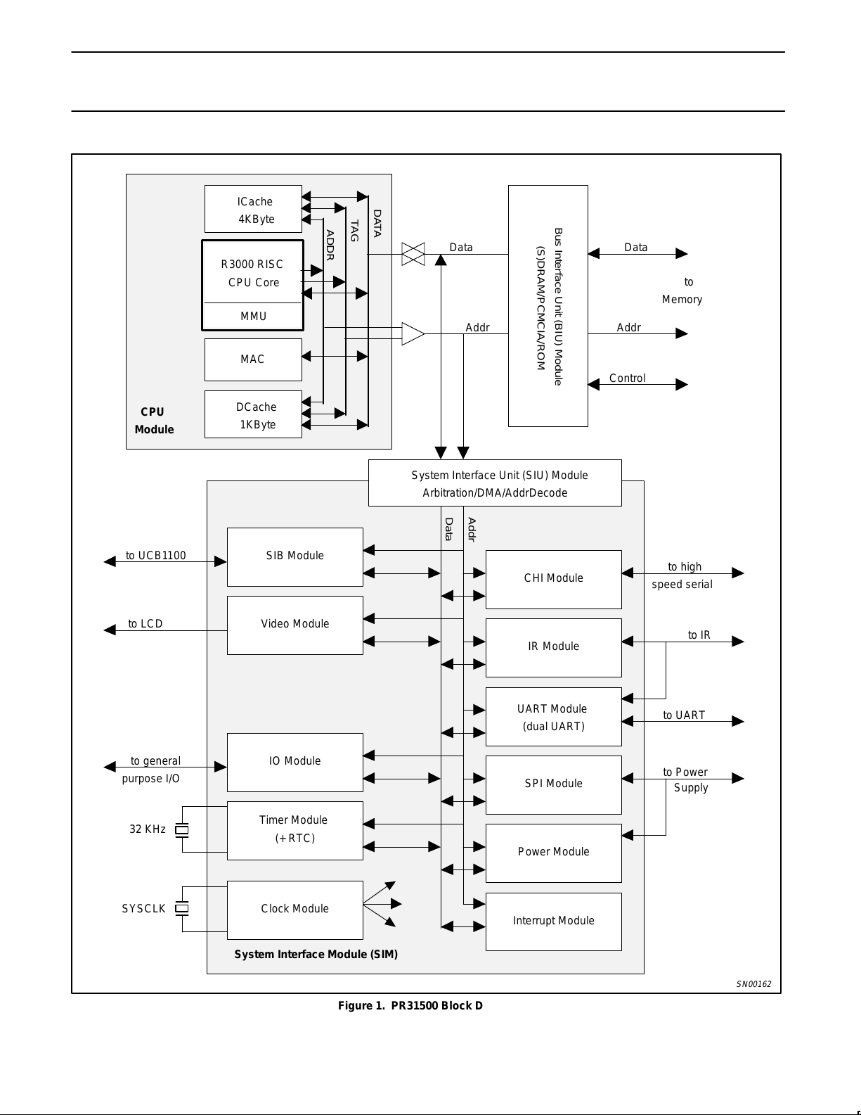
Figure 1 shows an External Block Diagram of PR31500.
FEATURES
•32-bit R3000 RISC static CMOS CPU
•4 KByte instruction cache
•1 KByte data cache
•Multiply/accumulator Instruction
•R3000A memory management unit with on-chip TLB
•Supports Big/Little Endian operating systems
•On-chip peripherals with individual power-down
– Multi-channel DMA controller
– Bus interface unit
– Memory controller for ROM, Flash, RAM, DRAM, SDRAM,
SRAM, and PCMCIA
– Power management module
– Video module
– Real-time clock 32.760KHz reference
– High-speed serial interface
– Infrared module
– Dual-UART
– SPI bus
•3.3V supply voltage
•208-pin LQFP (Low profile quad flat pack)
•40MHz operation frequency
ORDERING INFORMATION
PART NUMBER TEMPERATURE RANGE (°C) AND PACKAGE
FREQUENCY
(MHz)
DRAWING NUMBER
PR31500ABC 0 to +70, 208-pin Low Profile Quad Flat Pack 40 LQFP208
Philips Semiconductors Preliminary specification
MIPS
PR31500
Poseidon embedded processor
1996 Sep 24
3
R3000 RISC
CPU Core
ICache
4KByte
DCache
1KByte
Bus Interface Unit (BIU) Module
(S)DRAM/PCMCIA/ROM
Data
Addr
CHI Module
Addr
Data
Data
Addr
Control
to UCB1100
to LCD
to high
speed serial
to IR
Timer Module
(+ RTC)
IR Module
UART Module
(dual UART)
MAC
to UART
Power Module
SPI Module
to Power
Supply
IO Moduleto general
purpose I/O
32 KHz
SYSCLK
Interrupt Module
System Interface Module (SIM)
to
Memory
CPU
Module
DATA
TAG
ADDR
System Interface Unit (SIU) Module
Arbitration/DMA/AddrDecode
Video Module
SIB Module
MMU
Clock Module
SN00162
Figure 1. PR31500 Block Diagram

Philips Semiconductors Preliminary specification
MIPS
PR31500
Poseidon embedded processor
1996 Sep 24
4
OVERVIEW
Each of the on-chip peripherals consist of:
BIU Module
•System memory and PR31500 Bus Interface Unit (BIU)
– supports up to 2 banks of physical memory
– supports self-refreshing DRAM and SDRAM
– programmable parameters for each bank of DRAM or SDRAM
(row/column address configuration, refresh, burst modes, etc.)
•programmable chip select memory access
– 4 programmable (size, wait states, burst mode control) memory
device and general purpose chip selects
available for system ROM, SRAM, Flash
available for external port expansion registers
•supports up to 2 identical full PCMCIA ports
– PR31500 and UCB1100 provide the control signals and accepts
the status signals which conform to the PCMCIA version 2.01
standard
– appropriate connector keying and level-shifting buffers required
for 3.3V versus 5V PCMCIA interface implementations
SIU Module
•multi-channel 32-bit DMA controller and System Interface Unit
(SIU)
•independent DMA channels for video, SIB to/from UCB1100
audio/telecom codecs, high-speed serial port, IR UART, and
general purpose UART
•address decoding for submodules within System Interface Module
(SIM)
CPU Module
•R3000 RISC central processing unit core
– full 32-bit operation (registers, instructions, addresses)
– 32 general purpose 32-bit registers; 32-bit program counter
– MIPS RISC Instruction Set Architecture (ISA) supported
•on-chip cache
– 4 KByte direct-mapped instruction cache (I-cache)
physical address tag and valid bit per cache line
programmable burst size
instruction streaming mode supported
– 1 KByte data cache (D-cache)
physical address tag and valid bit per cache line
programmable burst size
write-through
– cache address snoop mode supported for DMA
– 4-level deep write buffer
•Memory Management Unit
– MIPS R3000A MMU contains on-chip TLB with:
32×64 bit wide entries
fully associative
2 entry micro TLB for very fast instruction address translation
Instruction address translation accesses full TLB after micro
TLB miss
Data address translation accesses full TLB
•high-speed multiplier/accumulator
– on-chip hardware multiplier
– supports 16x16 or 32x32 multiplier operations, with 64-bit
accumulator
– existing multiply instructions are enhanced and new multiply
and add instructions are added to R3000 instruction set to
improve the performance of DSP applications
•CPU interface
– handles data bus, address bus, and control interface between
CPU core and rest of PR31500 logic
Clock Module
•PR31500 supports system-wide single crystal configuration,
besides the 32 KHz RTC XTAL (reduces cost, power, and board
space)
•common crystal rate divided to generate clock for CPU, video,
sound, telecom, UARTs, etc.
•external system crystal rate is vendor-dependent
•independent enabling or disabling of individual clocks under
software control, for power management
CHI Module
•high-speed serial Concentration Highway Interface (CHI) contains
logic for interfacing to external full-duplex serial
time-division-multiplexed (TDM) communication peripherals
•supports ISDN line interface chips and other PCM/TDM serial
devices
•CHI interface is programmable (number of channels, frame rate,
bit rate, etc.) to provide support for a variety of formats
•supports data rates up to 4.096 Mbps
•independent DMA support for CHI receive and transmit
Interrupt Module
•contains logic for individually enabling, reading, and clearing all
PR31500 interrupt sources
•interrupts generated from internal PR31500 modules or from edge
transitions on external signal pins
IO Module
•contains support for reading and writing the 7 bi-directional
general purpose IO pins and the 32 bi-directional multi-function IO
pins
•each IO port can generate a separate positive and negative edge
interrupt
•independently configurable IO ports allow PR31500 to support a
flexible and wide range of system applications and configurations

Philips Semiconductors Preliminary specification
MIPS
PR31500
Poseidon embedded processor
1996 Sep 24
5
IR Module
•IR consumer mode
– allows control of consumer electronic devices such as stereos,
TVs, VCRs, etc.
– programmable pulse parameters
– external analog LED circuitry
•IRDA communication mode
– allows communication with other IRDA devices such as FAX
machines, copiers, printers, etc.
– supported by UART module within PR31500
– external analog receiver preamp and LED circuitry
– data rate = up to 115 Kbps at 1 meter
•IR FSK communication mode
– supported by UART module within PR31500
– external analog IR chip(s) perform frequency modulation to
generate the desired IR communication mode protocol
– data rate = up to 36000 bps at 3 meters
•carrier detect state machine
– periodically enables IR receiver to check if a valid carrier is
present
Power Module
•power-down modes for individual internal peripheral modules
•serial (SPI port) power supply control interface supported
•power management state machine has 4 states: RUNNING,
DOZING, SLEEP, and COMA
Serial Interconnect Bus (SIB) Module
•PR31500 contains holding and shift registers to support the serial
interface to the UCB1100 and/or other optional codec devices
•interface compatible with slave mode 3 of Crystal CS4216 codec
•synchronous, frame-based protocol
•PR31500 always master source of clock and frame frequency and
phase; programmable clock frequency
•each SIB frame consists of 128 clock cycles, further divided into 2
subframes or words of 64 bits each (supports up to 2 devices
simultaneously)
•independent DMA support for audio receive and transmit, telecom
receive and transmit
•supports 8-bit or 16-bit mono telecom formats
•supports 8-bit or 16-bit mono or stereo audio formats
•independently programmable audio and telecom sample rates
•CPU read/write registers for subframe control and status
System Peripheral Interface (SPI) Module
•provides interface to SPI peripherals and devices
•full-duplex, synchronous serial data transfers (data in, data out,
and clock signals)
•PR31500 supplies dedicated chip select and interrupt for an SPI
interface serial power supply
•8-bit or 16-bit data word lengths for the SPI interface
•programmable SPI baud rate
Timer Module
•Real Time Clock (RTC) and Timer
•40-bit counter (30.517 µsec granularity);
maximum uninterrupted time = 388.36 days
•40-bit alarm register (30.517 µsec granularity)
•16-bit periodic timer (0.868 µsec granularity);
maximum timeout = 56.8 msec
•interrupts on alarm, timer, and prior to RTC roll-over
UART Module
•2 independent full-duplex UARTs
•programmable baud rate generator
•UART-A port used for serial control interface to external IR
module
•UART-B port used for general purpose serial control interface
•UART-A and UART-B DMA support for receive and transmit
Video Module
•bit-mapped graphics
•supports monochrome, grey scale, or color modes
•time-based dithering algorithm for grey scale and color modes
•supports multiple screen sizes
•supports split and non-split displays
•variable size and relocatable video buffer
•DMA support for fetching image data from video buffer
Little/Big Endian Configuration
The PR31500 can be configures as a Big Endian or as a Little
Endian processor based on the /LB endian pin at power-up.
The byte ordering is as follows:
LITTLE ENDIAN BIG ENDIAN
D[31:24] D[7:0]
D[23:16] D[15:8]
D[15:8] D[23:16]
D[7:0] D[31:24]
/CAS3 /CAS0
/CAS2 /CAS1
/CAS1 /CAS2
/CAS0 /CAS3
Philips Semiconductors Preliminary specification
MIPS
PR31500
Poseidon embedded processor
1996 Sep 24
6
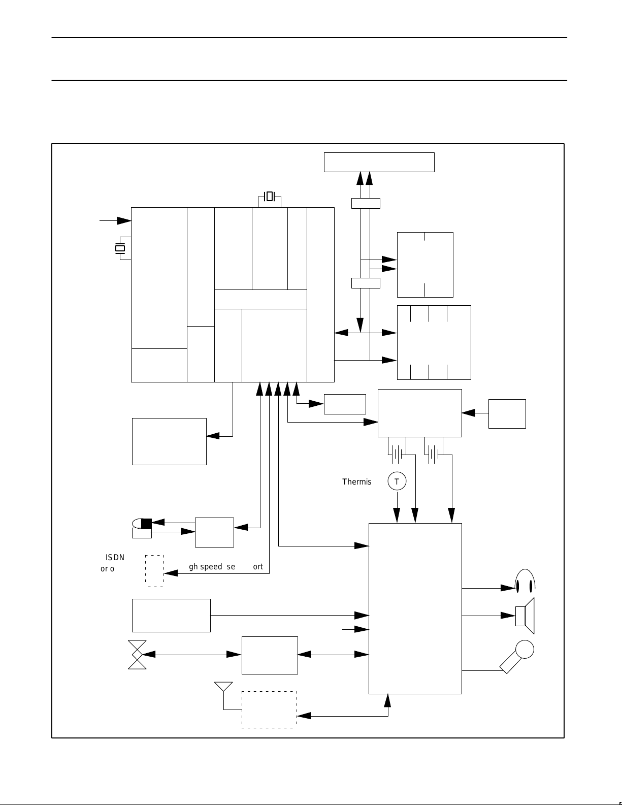
Figure 2 shows a typical system block diagram cosisting of
PR31500 and UCB1100 for a total system solution.
R3000
RISC
CPU
core
I–Cache/RAM
D–Cache/
RAM
32–bit Bus
LCD Interface
Timers
Real–time Clock
Serial I/F and
Magicbus
1–2 PCMCIA Slots
UCB1100
Main
Backup
(Lithium)
DAA
RF
Xceiver
or
Touchscreen
(Resistive)
Phone Jack
IR
PR31500
AC
Adapter
3.3V
Memory Protection
PCMCIA/ROM I/F
1–64 MBytes
ROM
1–16 MBytes
(S)DRAM
TThermistor
3.3V
32 KHz
SYSCLK
ID ROM
High speed serial port
ISDN
or other
peripherals
LCD
DRAM/SDRAM Interface
Power Supply
TLB
SN00163
Figure 2. System Block Diagram
Philips Semiconductors Preliminary specification
MIPS
PR31500
Poseidon embedded processor
1996 Sep 24
7
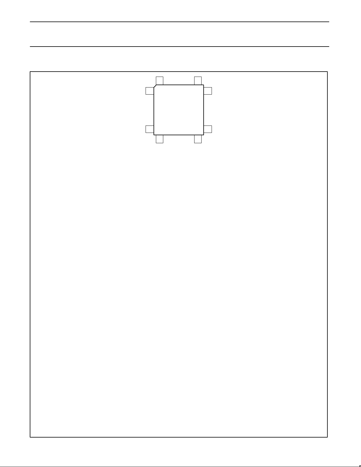
PIN CONFIGURATION
208
1
52
53 104
105
156
157
208-PIN
PLASTIC
QUAD FLAT PACK
TOP VIEW
Pin Function
1 V
DD
2 D(0) [D(24)]
3 V
SS
4 D(1) [D(25)]
5 D(2) [D(26)]
6 V
DD
7 D(3) [D(27)]
8 V
SS
9 D(4) [D(28)]
10 V
DD
11 D(5) [D(29)]
12 D(6) [D(30)]
13 V
SS
14 D(7) [D(31)]
15 V
SS
16 D(8) [D(16)]
17 V
DD
18 D(9) [D(17)]
19 D(10) [D(18)]
20 V
SS
21 D(11) [D(19)]
22 V
DD
23 D(12) [D(20)]
24 D(13) [D(21)]
25 V
SS
26 D(14) [D(22)]
27 D(15) [D(23)]
28 V
DD
29 /LB endian
30 MFIO(1)
31 –
32 –
33 V
SS
34 –
35 V
DD
36 V
DD
37 SIBMCLK
38 V
SS
39 SIBSCLK
40 SIBSYNC
41 SIBDIN
42 SIBDOUT
43 V
DD
44 SIBIRQ
45 MFIO(0)
46 IO(6)
47 IO(50
48 V
SS
49 chiclk
50 chifs
51 chidin
52 chidout
Pin Function
53 V
DD
54 RXD
55 TXD
56 IO(4)
57
58 IRIN
59 IROUT
60 V
SS
61 V
DD
62 CARDET
63 TXPWR
64 IO(3)
65 IO(2)
66 V
SS
67 SPICLK
68 SPIIN
69 SPIOUT
70 V
DD
71 TESTCPU
72 TESTIN
73 VIDDONE
74 TESTSIU
75 V
SS
76 VCC3
77 BC32K
78 V
DD
79 C32KIN
80 C32KOUT
81 V
SS
82 PWRCS
83 PWRINT
84 PWROK
85
86 ONBUTN
87 /PON
88 /CPURES
89 V
DD
90 DISPON
91 FRAME
92 V
SS
93 DF
94 LOAD
95 CP
96 V
SS
97 V
DD
98 VDAT(0)
99 VDAT(1)
100 VDAT(2)
101 VDAT(3)
102 V
SS
103 IO(1)
104 V
DD
Pin Function
105 /CARD2WAIT
106 /CARD2CSH
107 /CARD2CSL
108 IO(0)
109 V
SS
110 /IORD
111 /IOWR
112 /CARDREG
113 /CARD1WAIT
114 V
DD
115 MFIO(2)
116 V
DD
117 /CARD1CSL
118 /CARD1CSH
119 V
SS
120 /MCS3
121 /MCS2
122 /MCS1
123 /MCS0
124 /CS3
125 /CS2
126 /CS1
127 V
DD
128 SYSCLKIN
129 SYSCLKOUT
130 V
SS
131 V
SS
132 V
DD
133 D(31) [D(7)]
134 D(30) [D(6)]
135 V
SS
136 D(29) [D(5)]
137 V
DD
138 D(28) [D(4)]
139 D(27) [D(3)]
140 V
SS
141 D(26) [D(2)]
142 V
SS
143 D(25) [D(1)]
144 V
DD
145 D(24) [D(0)]
146 D(23) [D(15)]
147 V
DD
148 D(22) [D(14)]
149 V
SS
150 D(21) [D(13)]
151 V
DD
152 D(20) [D(12)]
153 D(19) [D(11)]
154 V
SS
155 D(18) [D(10)]
156 V
DD
Pin Function
157 D(17) [D(9)]
158 V
SS
159 D(16) [D(8)]
160 V
DD
161
162 /CS0
163 /RD
164 V
SS
165 V
DD
166 /DGRNT
167 /DREQ
168 ALE
169 /WE
170 V
DD
171 A(12)
172 A(11)
173 V
SS
174 A(10)
175 A(9)
176 V
DD
177 A(8)
178 A(7)
179 V
SS
180 A(6)
181 A(5)
182 V
DD
183 A(4)
184 V
SS
185 A(3)
186 A(2)
187 V
DD
188 A(1)
189 A(0)
190 V
SS
191 V
SS
192 /DCS0
193 /RAS1
194 /RAS0
195 /CAS3 [/CAS0]
196 V
DD
197 /CAS2 [/CAS1]
198 /CAS1 [/CAS2]
199 /CAS0 [/CAS3]
200 V
SS
201 V
DD
202 DCKE
203 V
SS
204 DCLKIN
205 DCLKOUT
206 V
DD
207 DQMH
208 DQML
NOTE: [ ] indicates the signal name in the Little Endian mode.
SN00164
Philips Semiconductors Preliminary specification
MIPS
PR31500
Poseidon embedded processor
1996 Sep 24
8
PIN DESCRIPTIONS
Overview
The PR31500 processor contains 208 pins consisting of input, output, bi-directional, and power and ground pins. These pins are used to
support various functions. The following sections will describe the function of each pin including any special power-down considerations for
each pin.
Pins
The PR31500 PROCESSOR contains 208 total pins, consisting of 136 signal pins, 4 spare pins, 34 power pins, and 34 ground pins. Of the 136
signal pins, 32 of them are multi-function and can be independently programmed either as IO ports or for an alternate standard/normal function.
As an IO port, any of these pins can be programmed as an input or output port, with the capability of generating a separate positive and
negative edge interrupt. See Section 2.3 for a summary of the multi-function IO ports versus their standard functions.
PIN #
NAME TYPE NAME AND FUNCTION
Memory Pins
D(31:0) I/O These pins are the data bus for the system. 8-bit SDRAMs should be connected to bits 7:0 and
16-bit SDRAMs and DRAMs should be connected to bits 15:0. All other 16-bit ports should be
connected to bits 31:16. Of course, 32-bit ports should be connected to bits 31:0. These pins are
normally outputs and only become inputs during reads, thus no resistors are required since the
bus will only float for a short period of time during bus turn-around.
A(12:0) O These pins are the address bus for the system. The address lines are multiplexed and can be
connected directly to SDRAM and DRAM devices. To generate the full 26-bit address for static
devices, an external latch must be used to latch the signals using the ALE signal. For static
devices, address bits 25:13 are provided by the external latch and address bits 12:0 (directly
connected from PR31500’s address bus) are held afterward by PR31500 processor for the
remainder of the address bus cycle.
168 ALE O This pin is used as the address latch enable to latch A(12:0) using an external latch, for generating
the upper address bits 25:13.
163 /RD O This pin is used as the read signal for static devices. This signal is asserted for reads from
/MCS3-0, /CS3-0, /CARD2CS and /CARD1CS for memory and attribute space, and for reads from
PR31500 processor accesses if SHOWPR31500 is enabled (for debugging purposes).
169 /WE O This pin is used as the write signal for the system. This signal is asserted for writes to /MCS3-0,
/CS3-0, /CARD2CS and /CARD1CS for memory and attribute space, and for writes to DRAM and
SDRAM.
199 /CAS0 (/WE0) O This pin is used as the CAS signal for SDRAMs, the CAS signal for D(7:0) for DRAMs, and the
write enable signal for D(7:0) for static devices.
198 /CAS1 (/WE1) O This pin is used as the CAS signal for D(15:8) for DRAMs and the write enable signal for D(15:8)
for static devices.
197 /CAS2 (/WE2) O This pin is used as the CAS signal for D(23:16) for DRAMs and the write enable signal for
D(23:16) for static devices.
195 /CAS3 (/WE3) O This pin is used as the CAS signal for D(31:24) for DRAMs and the write enable signal for
D(31:24) for static devices.
194 /RAS0 O This pin is used as the RAS signal for SDRAMs and the RAS signal for Bank0 DRAMs.
193 /RAS1 (/DCS1) O This pin is used as the chip select signal for Bank1 SDRAMs and the RAS signal for Bank1
DRAMs.
192 /DCS0 O This pin is used as the chip select signal for Bank0 SDRAMs.
202 DCKE O This pin is used as the clock enable for SDRAMs.
204 DCLKIN I This pin must be tied externally to the DCLKOUT signal and is used to match skew for the data
input when reading from SDRAM and DRAM devices.
205 DCLKOUT O This pin is the (nominal) 73.728 MHz clock for the SDRAMs.
207 DQMH O This pin is the upper data mask for a 16-bit SDRAM configuration.
208 DQML O This pin is the lower data mask for a 16-bit SDRAM or 8-bit SDRAM configuration.
124–126,
162
/CS3–0 O These pins are the Chip Select 3 through 0 signals. They can be configured to support either 32-bit
or 16-bit ports.
120–123 /MCS3–0 O These pins are the MagicCard Chip Select 3 through 0 signals. They only support 16-bit ports.
106, 107 /CARD2CSH,L O These pins are the Chip Select signals for PCMCIA card slot 2.
 Loading...