

Page 1

PNX2000
Audio video input processor
Rev. 03 – 23 August 2004 Product data
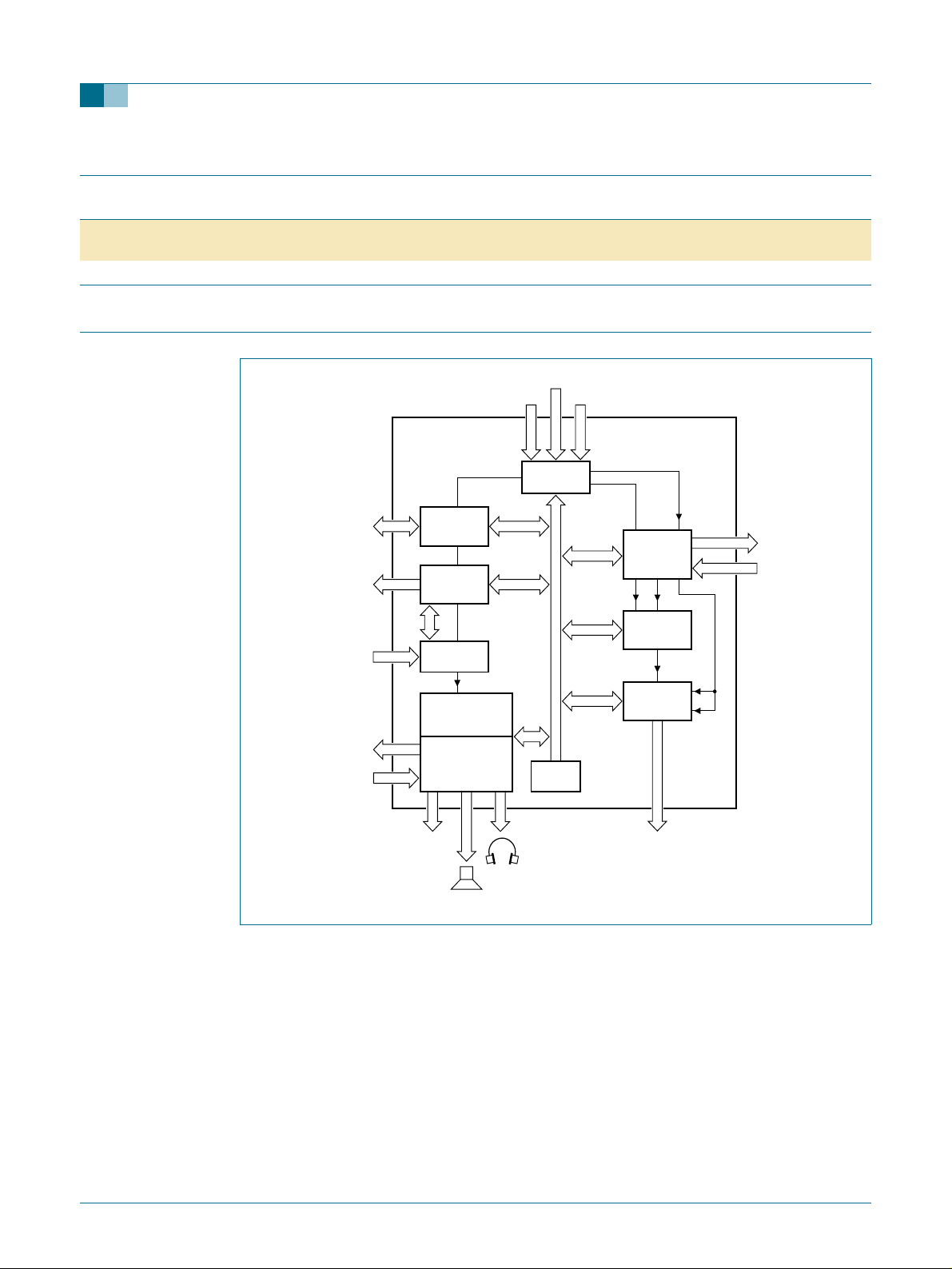
1. General description
The PNX2000 is a companion IC for use with the Nexperia™ 1 digital video home
entertainment engines such as PNX8526 and PNX8550.
The PNX2000 is always used in combination with the PNX3000.
PNX2000 is intended for mid to hi gh-end analog and hybrid TV sets, performing input
decoding of single stream analog audio and single stream analog video signals. In
addition, the PNX2000 is used for decoding and presentation of all audio output streams
in the system. Figure 1
2. Features
shows a block diagram of the device.
■ Detection of PAL, NTSC or SECAM, and various 1fH and 2fH component video input
■ Full support for 1f
■ Decoding for global VBI Standards (WST, WSS, VPS, CC, VITC).
■ ITU-656 output interface.
■ Global multi-standard audio demodulation and decoding.
■ Dolby Pro Logic II™
■ Advanced fully programmable audio post-processing functions, including
3. Applications
■ Analog TV receivers.
■ Hybrid TV receivers.
■ DVD recorders.
■ VCRs.
sources.
and 2fH video sources; progressive and interlaced.
H
2
multi-channel audio decoding and post-proce ssing.
psychoacoustic spatial algorithms for optimal loudspeaker matching.
1. Nexperia is a trademark of Koninklijke Philips Electronics N.V.
2. Dolby is a trademark of Dolby Laboratories
Page 2
Philips Semiconductors
PNX2000
Audio video input processor
4. Ordering information
Table 1: Ordering information
Type number Package
Description Version
name
PNX2000HL LQFP144 plastic low profile quad flat package; 144 leads; body 20 × 20 × 1.4 mm SOT486-1
5. Block diagram
DLINK2
DLINK1 DLINK3
2
C-bus
I
INT
13.5 MHz or
27 MHz
Xtal
2
6× I
S-bus
outputs
2
6× I
S-bus
inputs
PNX2000
audio data SIF or L/R
I2C-BUS
GTU
CLOCKS
DEMDEC DSP
AUDIO DSP
×4
PNX3000
interface
(2 stereo
or 4 mono)
video data CVBS, Y/C, YUV
54 MHz clock
I2D
×2×6
BCU
27 Msps or 54 Msps
PI-bus
VIDDEC
DCU
ITU-656
ITU-656
1f
or 2f
H
10-bit data
HSYNC
HSYNC/
VSYNC
mce559
H
Fig 1. Block diagram
9397 750 13928 © Koninklijke Philips Electronics N.V. 2004. All rights reserved.
Product data Rev. 03 – 23 August 2004 2 of 31
Page 3
Philips Semiconductors
7
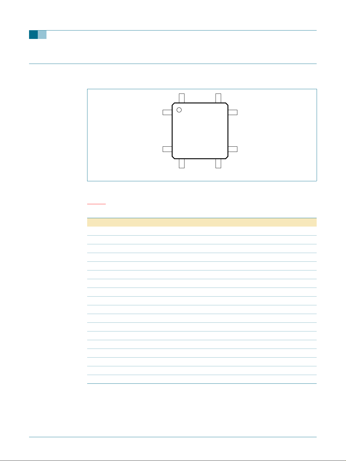
6. Pinning information
6.1 Pinning
PNX2000
Audio video input processor
Fig 2. Pin configuration
6.1.1 Pin description
Table 2 describes acronyms used in the pin tables:
Table 2: Acronym description
Acronym Description
3V 3.3 V LVCMOS
5VT 5 V tolerant inputs
Z3-state
TTL TTL logic
TTL-H TTL with hysteresis
CMOS CMOS logic
IA Input Analog
ID Input Digital
OD Output Digital
OA Output Analog
IOA I/O Analog
IOD I/O Digital
GA Ground Analog
SA Supply Analog
SD Supply Digital
OSCIN Crystal Oscillator Input
OSCOUT Crystal Oscillator Output
OSCGND Crystal Oscillator Ground
144
1
PNX2000HL
36
37
109
72
108
73
001aaa28
9397 750 13928 © Koninklijke Philips Electronics N.V. 2004. All rights reserved.
Product data Rev. 03 – 23 August 2004 3 of 31
Page 4

Philips Semiconductors
Table 3: Pins in numerical sequence
Pin Symbol Type Description
1V
2 DLINK1DP IA analog differential data link 1 positive termination
3 DLINK1DN IA analog differential data link 1 negative termination
4 DLINK1SP IA analog differential strobe link 1 positive termination
5 DLINK1SN IA analog differential strobe link 1 negative termination
7 DLINK2DP IA analog differential data link 2 positive termination
8 DLINK2DN IA analog differential data link 2 negative termination
9 DLINK2SP IA analog differential strobe link 2 positive termination
10 DLINK2SN IA analog differential strobe link 2 negative termination
12 DLINK3DP IA analog differential data link 3 positive termination
13 DLINK3DN IA analog differential data link 3 negative termination
14 DLINK3SP IA analog differential strobe link 3 positive termination
15 DLINK3SN IA analog differential strobe link 3 negative termination
16 V
17 I2C_ADR ID I
18 HSYNCFBL1 IA horizontal sync (external); fastblanking signal from
19 HSYNCFBL2 IA horizontal sync (external); fastblanking signal from
20 HVINFO OD horizontal and vertical sync information to PNX3000;
21 VSYNC1 ID vertical sync (external); TT L; 5VT
22 VSYNC2 ID vertical sync (external); TT L; 5VT
23 V
24 V
25 V
26 I2C_SCL IOD I
27 I2C_SDA IOD I
28 V
29 V
30 V
31 MPIFCLK OD 13.5 MHz or 27 MHz to PNX3000; CMOS
32 V
33 V
34 - n.c. not connected
35 V
36 V
37 V
38 XIN OSCIN crystal oscillator input
39 XOUT OSCOUT crystal oscillator output
40 XGND OSCGND crystal oscillator ground
SSD(I2D)
DDD(I2D)
DD3(DTC)
DDD(DTC)
SS(DTC)
SSE
SS
DDI
DDE
DDA(PLL)
DDI
SS
DDA(XTAL)
PNX2000
Audio video input processor
GD I2D digital ground
SD I2D digital 1.8 V supply voltage
2
C-bus address select (internal pull-down); TTL; 5VT
SCART
SCART
CMOS
SD DTC 3.3 V supply voltage
SD DTC 1.8 V supply voltage
GA DTC analog ground
2
C-bus clock; TTL; Z; 5VT
2
C-bus data; TTL; Z; 5VT
- 3.3 V ground
- 1.8 V ground
- 1.8 V supply voltage
- 3.3 V supply voltage
- phase locked loop 1.8 V supply voltage
- 1.8 V supply voltage
- 1.8 V ground
OSCVDD 1.8 V crystal oscillator supply voltage
9397 750 13928 © Koninklijke Philips Electronics N.V. 2004. All rights reserved.
Product data Rev. 03 – 23 August 2004 4 of 31
Page 5

Philips Semiconductors
Table 3: Pins in numerical sequence…continued
Pin Symbol Type Description
41 V
42 V
43 V
44 V
45 RESET_N IA external reset input
46 RESET_SEL ID selects between using an external reset input or using
47 DCLK OD reserved; CMOS
48 INTOUT OD interrupt line output; Z; 5VT
49 V
50 LL_CLK ID reserved; TTL; 5VT
51 DVO_CLK OD digital video output clock; CMOS; Z
52 DVO_VALID OD digital video data valid; CMOS; Z
53 V
54 V
55 DVO_DATA_0 OD digital video output state 0; CMOS; Z
56 DVO_DATA_1 OD digital video output state 1; CMOS; Z
57 DVO_DATA_2 OD digital video output state 2; CMOS; Z
58 DVO_DATA_3 OD digital video output state 3; CMOS; Z
59 V
60 DVO_DATA_4 OD digital video output state 4; CMOS; Z
61 DVO_DATA_5 OD digital video output state 5; CMOS; Z
62 DVO_DATA_6 OD digital video output state 6; CMOS; Z
63 DVO_DATA_7 OD digital video output state 7; CMOS; Z
64 DVO_DATA_8 OD digital video output state 8; CMOS; Z
65 DVO_DATA_9 OD digital video output state 9; CMOS; Z
66 V
67 V
68 V
69 I2S_OUT_SD3 OD I
70 I2S_OUT_SD3_WS OD I
71 I2S_OUT_SD3_SCK OD I
72 V
73 I2S_OUT_SD6 OD I
74 I2S_OUT_SD5 OD I
75 I2S_OUT_SD4 OD I
76 I2S_OUT_SD2 OD I
77 I2S_OUT_SD1 OD I
78 I2S_WS_SYS IOD I
79 I2S_SCK_SYS IOD I
80 V
PNX2000
Audio video input processor
SSE
DDI
SS
- 1.8 V supply voltage for KSFRAMs and KROMs
DDM
DDE
DDI
SS
SSE
DDE
DDI
SS
SSE
DDI
- 3.3 V ground
- 1.8 V supply voltage
- 1.8 V ground
internal POR; TTL; 5VT
- 3.3 V supply voltage
- 1.8 V supply voltage
- 1.8 V ground
- 3.3 V ground
- 3.3 V supply voltage
- 1.8 V supply voltage
- 1.8 V ground
2
S-bus data-out channel 3; CMOS
2
S-bus word select channel 3; CMOS
2
S-bus bit clock channel 3; CMOS
- 3.3 V ground
2
S-bus data out channel 6; CMOS
2
S-bus data out channel 5; CMOS
2
S-bus data out channel 4; CMOS
2
S-bus data out channel 2; CMOS
2
S-bus data out channel 1; CMOS
2
S-bus system word select; TTL-H; CMOS
2
S-bus system bit clock; TTL-H; CMOS
- 1.8 V supply voltage
9397 750 13928 © Koninklijke Philips Electronics N.V. 2004. All rights reserved.
Product data Rev. 03 – 23 August 2004 5 of 31
Page 6

Philips Semiconductors
PNX2000
Audio video input processor
Table 3: Pins in numerical sequence
…continued
Pin Symbol Type Description
81 V
82 V
SS
DDE
83 I2S_IN_SD6 ID I
84 I2S_IN_SD5 ID I
85 I2S_IN_SD4 ID I
86 I2S_IN_SD3 ID I
87 I2S_IN_SD2 ID I
88 I2S_IN_SD1 ID I
89 ADAC_CLK OD Used for 128 f
- 1.8 V ground
- 3.3 V supply voltage
2
S-bus data in channel 6; TTL; 5VT
2
S-bus data in channel 5; TTL; 5VT
2
S-bus data in channel 4; TTL; 5VT
2
S-bus data in channel 3; TTL; 5VT
2
S-bus data in channel 2; TTL; 5VT
2
S-bus data in channel 1; TTL; 5VT
or 256 fs clock output to external audio
s
DAC; CMOS.
90 - n.c. not connected
91 V
DDE
- 3.3 V supply voltage
92 TDI ID JTAG test data in; TTL-H; 5VT
93 TDO OD JTAG test data out; CMOS
94 TCK ID JTAG test clock; TTL-H; 5VT
95 TMS ID JTAG test mode select; TTL-H; 5VT
96 TRST_N ID JTAG reset (active low); TTL-H; 5VT
97 V
98 V
99 V
100 V
101 V
102 V
DDI
SS
SSE
SS(ADAC)
DDD(ADAC)
DDA(ADAC)
- 1.8 V supply voltage
- 1.8 V ground
- 3.3 V ground
GD audio DAC 1.8 V digital ground
SD audio DAC 1.8 V digital supply voltage
SA audio DAC 3.3 V supply voltage
103 ADAC1_P SA Positive analog reference derived via emitter follower
from PNX3000 V_SND pin.
104 ADAC1 OA analog audio output 1
105 ADAC1_N GA Negative analog reference star connected at
PNX3000.
106 ADAC2_N GA Negative analog reference star connected at
PNX3000.
107 ADAC2 OA analog audio output 2
108 ADAC2_P SA Positive analog reference derived via emitter follower
from PNX3000 V_SND pin.
109 ADAC3_P SA Positive analog reference derived via emitter follower
from PNX3000 V_SND pin.
110 ADAC3 OA analog audio output 3
111 ADAC3_N GA Negative analog reference star connected at
PNX3000.
112 ADAC4_N GA Negative analog reference star connected at
PNX3000.
113 ADAC4 OA analog audio output 4
114 ADAC4_P SA Positive analog reference derived via emitter follower
from PNX3000 V_SND pin.
9397 750 13928 © Koninklijke Philips Electronics N.V. 2004. All rights reserved.
Product data Rev. 03 – 23 August 2004 6 of 31
Page 7

Philips Semiconductors
PNX2000
Audio video input processor
Table 3: Pins in numerical sequence
Pin Symbol Type Description
115 ADAC5_P SA Positive analog reference derived via emitter follower
116 ADAC5 OA analog audio output 5
117 ADAC5_N GA Negative analog reference star connected at
118 ADAC6_N GA Negative analog reference star connected at
119 ADAC6 OA analog audio output 6
120 ADAC6_P SA Positive analog reference derived via emitter follower
121 ADAC7_P SA Positive analog reference derived via emitter follower
122 ADAC7 OA analog audio output 7
123 ADAC7_N GA Negative analog reference star connected at
124 ADAC8_N GA Negative analog reference star connected at
125 ADAC8 OA analog audio output 8
126 ADAC8_P SA Positive analog reference derived via emitter follower
127 ADAC9_P SA Positive analog reference derived via emitter follower
128 ADAC9 OA analog audio output 9
129 ADAC9_N GA Negative analog reference star connected at
130 ADAC10_N GA Negative analog reference star connected at
131 ADAC10 OA analog audio output 10
132 ADAC10_P SA Positive analog reference derived via emitter follower
133 ADAC11_P SA Positive analog reference derived via emitter follower
134 ADAC11 OA analog audio output 11
135 ADAC11_N GA Negative analog reference star connected at
136 ADAC12_N GA Negative analog reference star connected at
137 ADAC12 OA analog audio output 12
138 ADAC12_P SA Positive analog reference derived via emitter follower
139 V
140 V
141 V
SS
- 1.8 V supply voltage for KSFRAMs and KROMs
DDM
DDE
- 1.8 V ground
- 3.3 V supply voltage
…continued
from PNX3000 V_SND pin.
PNX3000.
PNX3000.
from PNX3000 V_SND pin.
from PNX3000 V_SND pin.
PNX3000.
PNX3000.
from PNX3000 V_SND pin.
from PNX3000 V_SND pin.
PNX3000.
PNX3000.
from PNX3000 V_SND pin.
from PNX3000 V_SND pin.
PNX3000.
PNX3000.
from PNX3000 V_SND pin.
9397 750 13928 © Koninklijke Philips Electronics N.V. 2004. All rights reserved.
Product data Rev. 03 – 23 August 2004 7 of 31
Page 8

Philips Semiconductors
PNX2000
Audio video input processor
Table 3: Pins in numerical sequence
Pin Symbol Type Description
142 V
143 V
144 V
SSE
DDE
SSE
- 3.3 V ground
- 3.3 V supply voltage
- 3.3 V ground
…continued
In the tables that follo w , signals of the PNX2000 hav e been sorted by functional group. For
quick reference Table 4
Table 4: Signal group s
Functional group Table number
2
D-bus Table 5
I
AUDIO Table 6
I2S-bus Table 7
VIDDEC Table 8
ITU-656 Table 9
JTAG Table 10
I2C-bus Table 11
CLOCK Table 12
GTU Table 13
RESET Table 14
DIGITAL SUPPLY Table 15
ANALOG SUPPLY Table 16
identifies each functional group and associated table.
Table 5: I2D pins
Symbol Pin Type Description
DLINK1DP 2 IA analog differential data link 1 positive termination
DLINK1DN 3 IA analog differential data link 1 negative term ination
DLINK1SP 4 IA analog differential strobe link 1 positive termination
DLINK1SN 5 IA analog differential strobe link 1 negative termination
DLINK2DP 7 IA analog differential data link 2 positive termination
DLINK2DN 8 IA analog differential data link 2 negative term ination
DLINK2SP 9 IA analog differential strobe link 2 positive termination
DLINK2SN 10 IA analog differential strobe link 2 negative termination
DLINK3DP 12 IA analog differential data link 3 positive termination
DLINK3DN 13 IA analog differential data link 3 negative termination
DLINK3SP 14 IA analog differential strobe link 3 positive termination
DLINK3SN 15 IA analog differential strobe link 3 negative termination
Table 6: Audio pins
Symbol Pin Type Description
ADAC1 104 OA analog audio output 1
ADAC2 107 OA analog audio output 2
ADAC3 110 OA analog audio output 3
ADAC4 113 OA analog audio output 4
9397 750 13928 © Koninklijke Philips Electronics N.V. 2004. All rights reserved.
Product data Rev. 03 – 23 August 2004 8 of 31
Page 9

Philips Semiconductors
PNX2000
Audio video input processor
Table 6: Audio pins
Symbol Pin Type Description
ADAC5 116 OA analog audio output 5
ADAC6 119 OA analog audio output 6
ADAC7 122 OA analog audio output 7
ADAC8 125 OA analog audio output 8
ADAC9 128 OA analog audio output 9
ADAC10 131 OA analog au dio output 10
ADAC11 134 OA analog au dio output 11
ADAC12 137 OA analog au dio output 12
ADAC1_P 103 SA Positive analog reference derived via emitter follower from
ADAC1_N 105 GA Negative analog reference star connected at PNX3000.
ADAC2_P 108 SA Positive analog reference derived via emitter follower from
ADAC2_N 106 GA Negative analog reference star connected at PNX3000.
ADAC3_P 109 SA Positive analog reference derived via emitter follower from
ADAC3_N 111 GA Negative analog reference star connected at PNX3000.
ADAC4_P 114 SA Positive analog reference derived via emitter follower from
ADAC4_N 112 GA Negative analog reference star connected at PNX3000.
ADAC5_P 115 SA Positive analog reference derived via emitter follower from
ADAC5_N 117 GA Negative analog reference star connected at PNX3000.
ADAC6_P 120 SA Positive analog reference derived via emitter follower from
ADAC6_N 118 GA Negative analog reference star connected at PNX3000.
ADAC7_P 121 SA Positive analog reference derived via emitter follower from
ADAC7_N 123 GA Negative analog reference star connected at PNX3000.
ADAC8_P 126 SA Positive analog reference derived via emitter follower from
ADAC8_N 124 GA Negative analog reference star connected at PNX3000.
ADAC9_P 127 SA Positive analog reference derived via emitter follower from
ADAC9_N 129 GA Negative analog reference star connected at PNX3000.
ADAC10_P 132 SA Positive analog reference derived via emitter follower from
ADAC10_N 130 GA Negative analog reference star connected at PNX3000.
ADAC11_P 133 SA Positive analog reference derived via emitter follower from
ADAC11_N 135 GA Negative analog reference star connected at PNX3000.
ADAC12_P 138 SA Positive analog reference derived via emitter follower from
ADAC12_N 136 GA Negative analog reference star connected at PNX3000.
…continued
PNX3000 V_SND pin.
PNX3000 V_SND pin.
PNX3000 V_SND pin.
PNX3000 V_SND pin.
PNX3000 V_SND pin.
PNX3000 V_SND pin.
PNX3000 V_SND pin.
PNX3000 V_SND pin.
PNX3000 V_SND pin.
PNX3000 V_SND pin.
PNX3000 V_SND pin.
PNX3000 V_SND pin.
9397 750 13928 © Koninklijke Philips Electronics N.V. 2004. All rights reserved.
Product data Rev. 03 – 23 August 2004 9 of 31
Page 10

Philips Semiconductors
Table 7: I2S-bus pins
Symbol Pin Type Description
I2S_IN_SD1 88 ID I
I2S_IN_SD2 87 ID I
I2S_IN_SD3 86 ID I
I2S_IN_SD4 85 ID I
I2S_IN_SD5 84 ID I
I2S_IN_SD6 83 ID I
I2S_OUT_SD1 77 OD I
I2S_OUT_SD2 76 OD I
I2S_OUT_SD4 75 OD I
I2S_OUT_SD5 74 OD I
I2S_OUT_SD6 73 OD I
I2S_OUT_SD3_SCK 71 OD I
I2S_OUT_SD3_WS 70 OD I
I2S_OUT_SD3 69 OD I
I2S_SCK_SYS 79 IOD I
I2S_WS_SYS 78 IOD I
ADAC_CLK 89 OD Used for 128 f
PNX2000
Audio video input processor
2
S-bus data in channel 1; TTL; 5VT
2
S-bus data in channel 2; TTL; 5VT
2
S-bus data in channel 3; TTL; 5VT
2
S-bus data in channel 4; TTL; 5VT
2
S-bus data in channel 5; TTL; 5VT
2
S-bus data in channel 6; TTL; 5VT
2
S-bus data out channel 1; CMOS
2
S-bus data out channel 2; CMOS
2
S-bus data out channel 4; CMOS
2
S-bus data out channel 5; CMOS
2
S-bus data out channel 6; CMOS
2
S-bus bit clock channel 3; CMOS
2
S-bus word select channel 3; CMOS
2
S-bus data-out channel 3; CMOS
2
S-bus system bit clock; TTL-H; CMOS
2
S-bus system word select; TTL-H; CMOS
or 256 fs clock output to external audio
DAC; CMOS.
s
Table 8: VIDDEC pins
Symbol Pin Type Description
HVINFO 20 OD horizontal and vertical sync information to PNX3000; CMOS
HSYNCFBL1 18 IA horizontal sync (external); fastblanking signal from SCART
HSYNCFBL2 19 IA horizontal sync (external); fastblanking signal from SCART
VSYNC1 21 ID vertical sync (external); TTL; 5VT
VSYNC2 22 ID vertical sync (external); TTL; 5VT
Table 9: ITU-656 pins
Symbol Pin Type Description
DVO_DATA_0 55 OD digital video output state 0; CMOS; Z
DVO_DATA_1 56 OD digital video output state 1; CMOS; Z
DVO_DATA_2 57 OD digital video output state 2; CMOS; Z
DVO_DATA_3 58 OD digital video output state 3; CMOS; Z
DVO_DATA_4 60 OD digital video output state 4; CMOS; Z
DVO_DATA_5 61 OD digital video output state 5; CMOS; Z
DVO_DATA_6 62 OD digital video output state 6; CMOS; Z
DVO_DATA_7 63 OD digital video output state 7; CMOS; Z
DVO_DATA_8 64 OD digital video output state 8; CMOS; Z
DVO_DATA_9 65 OD digital video output state 9; CMOS; Z
9397 750 13928 © Koninklijke Philips Electronics N.V. 2004. All rights reserved.
Product data Rev. 03 – 23 August 2004 10 of 31
Page 11

Philips Semiconductors
PNX2000
Audio video input processor
Table 9: ITU-656 pins
…continued
Symbol Pin Type Description
DVO_ VALID 52 OD digital video data valid; CMOS; Z
DVO_ CLK 51 OD digital video output clock; CMOS; Z
LL_CLK 50 ID reserved; TTL; 5VT
[1] It is recommended to bias this pad with a 10 kΩ resistor
[1]
Table 10: JTAG pins
Symbol Pin Type Description
TDO 93 OD JTAG test data out; CMOS
TDI 92 ID JTAG test data in; TTL-H; 5VT
TCK 94 ID JTAG test clock; TTL-H; 5VT
[1]
TRST_N
96 ID JTAG reset (active low); TTL-H; 5VT
TMS 95 ID JTAG test mode select; TTL-H; 5VT
[1] It is recommended to pull-down TRST_N with a 10 kΩ resistor. This ensures correct reset state of internal
TAP circuitry and correct POR of the device within defined state machine.
Table 11: I2C-bus pins
Symbol Pin Type Description
2
I2C_SDA 27 IOD I
I2C_SCL 26 IOD I
I2C_ADR 17 ID I
C-bus data; TTL; Z; 5VT
2
C-bus clock; TTL; Z; 5VT
2
C-bus address select (internal pull-down); TTL; 5VT
Table 12: Clock pins
Symbol Pin Type Description
MPIFCLK 31 OD 13.5 MHz or 27 MHz to PNX3000; CMOS
DCLK 47 OD reserved; CMOS
XIN 38 OSCIN crystal oscillator input
XOUT 39 OSCOUT crystal oscillator output
XGND 40 OSCGND crystal oscillator ground
Table 13: GTU pins
Symbol Pin Type Description
INTOUT 48 OD interrupt line output; Z; 5VT
Table 14: Reset pins
Symbol Pin Type Description
RESET_N 45 IA external reset input
RESET_SEL 46 ID selects between using an external reset input or using
internal POR; TTL; 5VT
HIGH = internal reset
LOW = external reset
9397 750 13928 © Koninklijke Philips Electronics N.V. 2004. All rights reserved.
Product data Rev. 03 – 23 August 2004 11 of 31
Page 12

Philips Semiconductors
Table 15: Digital supply pins
Symbol Pin Type Description
V
DDE
V
SSE
[1]
V
DDI
V
SS
[1]
V
DDM
V
SSD(I2D)
V
DDD(I2D)
V
SS(ADAC)
V
DDD(ADAC)
V
DD3(DTC)
V
DDD(DTC)
[1] V
DDI
PNX2000
Audio video input processor
32,49,66, 82,91,
141,143
28,41,59, 72,99,
142,144
30,35,53,67, 80,97 - 1.8 V supply voltage
29,36,43, 54,68,81,
98,139
44,140 - 1.8 V supply voltage for KSFRAMs and KROMs
1GDI
16 SD I2D digital 1.8 V supply voltage
100 GD audio DAC 1.8 V digital ground
101 SD audio DAC 1.8 V digital supply voltage
23 SD DTC 3.3 V supply voltage
24 SD DTC 1.8 V supply voltage
and V
can be connected to same 1.8 V supply voltage.
DDM
- 3.3 V supply voltage
- 3.3 V ground
- 1.8 V ground
2
D digital ground
Table 16: Analog supply pins
Symbol Pin Type Description
V
SSA(I2D)
V
DDA(I2D)
V
DDA(PLL)
V
DDA(ADAC)
V
SS(DTC)
V
DDA(XTAL)
6GA I2D analog ground
11 SA I2D analog 1.8 V supply voltage
33 - phase locked loop 1.8 V supply voltage
102 SA audio DAC 3.3 V supply voltage
25 GA DTC analog ground
37 OSCVDD 1.8 V crystal oscillator supply voltage
7. Functional description
7.1 Overview
Table 17 describes the functions of the hardware blocks (see also PNX2000 Block
Diagram Figure 1
For more detailed functional description refer to the PNX2000 User Manual.
Table 17: Block function
Function Block Description
High speed data link I
Video decoder
processor
Serial interface I
Global Task Unit GTU Generates all the internal clocks, reset and power
).
2
D Receives data in three streams from PNX3000.
VIDDEC Decodes and processes CVBS, YUV or Y/C in YUV
stream.
2
C-bus To access all the internal registers.
management.
9397 750 13928 © Koninklijke Philips Electronics N.V. 2004. All rights reserved.
Product data Rev. 03 – 23 August 2004 12 of 31
Page 13

Philips Semiconductors
PNX2000
Audio video input processor
Table 17: Block function
Function Block Description
TV sound decoder DEMDEC
Audio processor AUDIO DSP Processing analog and digital audio sources.
Data Capture Unit DCU Acquires VBI data (Teletext; CC; VPS) and formats in a
Formatter unit ITU-656 Formats YUV, VBI data and CVBS data in ITU-656.
Bus Control Unit BCU Bus arbitration among all the internal bloc ks.
…continued
DSP
Demodulation, decoding of terrestrial TV audio standards
.
stream.
7.2 Interfaces
Table 18: Interfaces
Interface Description
2
C-bus The PNX2000 IC is controlled using an I2C-bus. It performs like an I2C-bus to PI-bus
I
bridge, i.e. translates I
2
D Receives data in three streams from PNX3000.
I
2
S-bus Serial digital audio interface (6 stereo inputs, 6 stereo outputs) for connection to other
I
devices that support the I2S-bus standard. Can be used to receive decoded sound
from a multi-channel digital audio decoder, provide additional ADCs and DACs , or loop
audio signals through an external processor or delay line.
ITU-656 Mainly intended to transfer output data stream externally to the PNX8550, but the
output data stream could also be readable by other ITU-656 input devices that
implement data valid signalling.
DACS Digital-analog converters used to generate analog outputs from Sound Core.
2
C-bus slave received commands to PI-bus master commands.
7.3 Features in detail
7.3.1 Video
• Automatic Gain Control (AGC) to correct amplitude errors at input source.
• Synchronization identification (used for channel search).
• Sync processing for 1f
• Standard detection of PAL, NTSC or SECAM and various 1f
video input sources.
video
1f
H
and 2fH video input source.
H
and 2fH component
H
• Color decoding (ITU-601) for PAL, NTSC or SECAM input sources.
• 2D comb filtering.
• Support for component video sources with sync on CVBS or green.
• Fastblank insertion of RGB signals onto CVBS input.
2f
video
H
• Support for various progressive and interlaced component video sources.
• Synchronization of video sources with sync on Y or external H/V inputs.
VBI data capture
9397 750 13928 © Koninklijke Philips Electronics N.V. 2004. All rights reserved.
Product data Rev. 03 – 23 August 2004 13 of 31
Page 14

Philips Semiconductors
• Decoding of 525 line standards; WST, WSS, VPS, CC, VITC.
• Decoding of 625 line standards; WST, WSS, CC, VITC.
ITU-656 output interface
• Video and VBI formatting into ITU-style output data stream, compliant to
ITU-656/1364 (exception being the use of a data valid signal).
• Interfacing to PNX8550 IC.
• Support for CVBS/C mode to interface to external picture improvement devices.
7.3.2 Audio
Demodulator and decoder
• Demodulator and Decoder Easy Programming (DDEP).
• Auto Standard Detection (ASD).
• Static Standard Selection (SSS).
• DQPSK demodulation for different standards, simultaneously with 1-channel FM
demodulation.
• NICAM decoding (B/G, I, D/K and L standard).
• Two-carrier multi-standard FM demodulation (B/G, D/K and M standard).
• Decoding for three analog multi-channel systems (A2, A2+ and A2*) and satellite
sound.
• Adaptive de-emphasis for satellite FM.
• Optional AM demodulation for system L, simultaneously with NICAM.
• Identification A2 systems (B/G, D/K and M standard) with different identification time
constants.
• FM pilot carrier present detector.
• Monitor selection for FM/AM DC values and signals, with peak and quasi peak
detection option.
• BTSC MPX decoding.
• SAP decoding.
• dbx
• Japan (EIAJ) decoding.
• FM radio decoding.
• Soft muting for DEMDEC outputs DEC, MONO and SAP.
• FM over modulation adaptation option to avoid clipping and distortion.
• Sample Rate Conversion (SRC) for up to three demodulated terrestrial audio signals.
Allows processing of SCART and demodulated terrestrial signals.
® 3
TV noise reduction.
PNX2000
Audio video input processor
Audio multi-channel decoder
• Dolby Pro Logic II™
3. dbx is a registered trademark of Carillon Electronics Corp.
9397 750 13928 © Koninklijke Philips Electronics N.V. 2004. All rights reserved.
Product data Rev. 03 – 23 August 2004 14 of 31
Page 15

Philips Semiconductors
• 6-channel pr ocessing for Main Left and Main Right, Subwoof er, Center, Surround Left
and Surround Right.
Volume and tone control
• Automatic Volume Level (AVL) control.
• Smooth volume control.
• Master volume control and balance.
• Soft mute.
• Loudness.
• Bass, treble.
• Dynamic Bass Enhancement (DBE).
• Dynamic ULTRABASS (DUB).
• Non-processed subwoofer.
• 5-band equalizer.
• Acoustical compensation.
• Programmable beeper.
• Noise generation for loudspeaker level trimming.
PNX2000
Audio video input processor
Reflection and delay
• Dolby Pro Logic II™ delay.
• Pseudo hall/matrix function.
Psychoacoustic spatial algorithms, downmix and split
• Incredible Mono.
• Incredible Stereo.
• Virtual Dolby Surround™.
• Virtual Dolby Digital™.
• Bass Redirection according to Dolby™ specifications.
• BBE
Interfaces and switching
®
Sound Processing
• Digital audio input interface (stereo I
• Digital audio output interface (stereo I
4
2
S-bus input interface).
2
S-bus output interface).
• Digital crossbar switch for all digital signal sources and destinations.
• Output crossbar for exchange of channel processing functionality.
• Voice recognition output interface (stereo I
2
S-bus output interface).
• Audio monitoring for level detection.
• Eight audio DACs for 6-channel loudspeaker outputs and stereo headphones output.
• Four audio DACs for stereo SCART output and stereo LINE output.
4. BBE is a registered trademark of BBE Sound Inc. See Section 18.
9397 750 13928 © Koninklijke Philips Electronics N.V. 2004. All rights reserved.
Product data Rev. 03 – 23 August 2004 15 of 31
Page 16

Philips Semiconductors
• Serial data link interfacing for analog multi-purpose interface PNX3000.
8. Television application
Figure 3 shows an overview of the top level hardware architecture of a TV application,
using the PNX3000 and PNX2000 as an analog front-end and the PNX8550 as the main
processor. This system is aimed at the hybrid (analog or digital) TV market.
The main SOC in the system, PNX8550, performs key features for high quality television
like video quality enhancement, motion comp ensation and picture-in-picture processing.
PNX2000 together with PNX3000 are used to perform the input decoding of a single
stream of analog audio and a single stream of analog video (1f
PNX2000 performs the following main functions:
PNX2000
Audio video input processor
or 2fH) broadcast signals.
H
TUNERS
UV1316
SCART
UV13361
21
20
19
21
18
16
14
12
10
8
6
4
2
20
17
18
15
16
13
14
11
12
10
8
6
4
2
19
17
15
13
11
9
7
5
3
1
CVBS Y/C
RGB 2
L/R audio 2
CVBS 1
L/R audio 1
status
LEVEL ADJUSTMENT
REMOTE CONTROL
LOCAL KEYPAD
• Color decoding into ITU-601 compatible format (1f
or 2fH).
H
• A digital inte rface to external 3D comb filter.
• VBI data capture (Teletext, WSS, CC) .
• ITU-656 formatting for communication to PNX8550.
• Audio demodulation and decoding.
• Audio processing and D-A conversion.
The audio data is transferred between PNX2000 and PNX8550 using I
and PNX3000 are controlled from PNX8550 via the I
CVBS
SIF
VIF
PNX3000
STANDBY
CONTROLLER
I2D
L/R
audio
MICRO-
PNX2000
YUV (656)
audio I
audio I
(2×)
audio I
(3×)
2
S-bus
2
S-bus
2
S-bus
PNX8550
32-bit
8-bit or 16-bit
2
C-bus.
RGB
10 bits (3×)
DISPLAY
PROCESSOR
DDR
16 Mb
FLASH
ROM
18 Mb
RGB
AMPLIFIER
DEFL.
CONT.
AUDIO
AMPLIFIER
2
S-bus. PNX2000
mce558
Fig 3. TV application
9397 750 13928 © Koninklijke Philips Electronics N.V. 2004. All rights reserved.
Product data Rev. 03 – 23 August 2004 16 of 31
Page 17

Philips Semiconductors
PNX2000
Audio video input processor
9. Limiting values
Permanent damage may occur if absolute maximum ratings are exceeded. Prolonged
operation at maximum rating may significantly reduce the reliability of the product.
Table 19: Absolute maximum ratings
Ratings are valid only within operating temperature range unless otherwise specified. All voltages are with respect to V
unless otherwise stated.
Symbol Parameter Min Max Unit
V
DD(core)
V
DD(I/O)
V
I
V
I
I
latchup
V
esd
V
esd
T
stg
supply voltage −0.5 +2.5 V
supply voltage −0.5 +4.6 V
DC input voltage (
[1] [2]
DC input voltage 5V tolerant I/O pins (
latch-up current (
[4]
)100-mA
electrostatic discharge voltage HBM (
electrostatic discharge voltage MM (
[3]
and
) −0.5 V
[2]
[3]
and
) −0.5 +6 V
[5]
[7]
and
)-±2kV
[6]
[7]
and
)-±200 V
+ 0.5 V
DD(I/O)
storage temperature −40 +125 °C
SS
[1] Not to exceed 4.6 V.
[2] Including voltage on outputs in 3-state mode.
[3] Only valid when the V
[4] Valid for : −(0.5 × V
[5] Human Body Model, I
[6] Machine Model 0.5 mH, I
[7] This product includes circuits specifically designed for the protection of its internal devices from the damaging effects of excessive static
charge. However, it is suggested that conventional precautions be taken to avoid applying voltages greater than the rated maximum.
DD
supply voltage is present.
DD(I/O)
) < V < +(1.5 × VDD); Tj < 125 °C.
< 1 mA.
leak
< 1 mA.
leak
10. Characteristics
10.1 Static characteristics
Table 20: Static characteristics: power supply pins
= 0 °C to +70 °C to commercial unless otherwise specified.
T
amb
Symbol Parameter Conditions Min Typ Max Unit
1.8V Power Supply Pins: V
V
DD(core)
I
DD(core)
supply voltage, 1.8 V supplies - 1.65 1.8 1.95 V
supply current, 1.8 V supplies V
DDI
, V
DDM
, V
DDD(I2D)
, V
DDA(I2D)
, V
DDA(PLL)
, V
DDA(XTAL)
= 1.8 V - 250 - mA
DD(core)
, V
DDD(ADAC)
, V
DDD(DTC)
3.3V Power Supply Pins: V
V
DD(3V3)
I
DD(3V3)
9397 750 13928 © Koninklijke Philips Electronics N.V. 2004. All rights reserved.
Product data Rev. 03 – 23 August 2004 17 of 31
supply voltage, 3.3 V supplies - 3.0 3.3 3.6 V
supply current, 3.3 V supplies V
DDE
, V
DD3(DTC)
, V
DDA(ADAC)
= 3.3 V - 50 - mA
DD(core)
Page 18

Philips Semiconductors
PNX2000
Audio video input processor
Table 21: Static characteristics: digital pins
= 0 °C to +70 °C to commercial unless otherwise specified.
T
amb
Symbol Parameter Conditions Min Typ Max Unit
2
S inputs: I2S_IN_SD1-6, I2C Address: I2C_ADR
I
I
IL
V
I
V
IH
V
IL
I
PD
External Sync: VSYNC1, VSYNC2, Reset: RESET_SEL, ITU-656: LL_CLK
I
IL
I
IH
V
I
V
IH
V
IL
Jtag inputs: TDI, TCK, TRST_N, TMS
I
IH
V
I
V
IH
V
IL
V
hys
I
PU
2
C Pins: I2C_SDA, I2C_SCL
I
C
I
I
LI
I
IN(MAX)
V
I
V
IL
V
IH
V
OL
I
OL
ITU-656 Outputs: DVO_DATA_0-9, DVO _VALID, DVO_CLK
I
oz
V
I
V
OH
V
OL
I
OH
I
OL
I
OH
I
OL
2
S I/O: I2S_SCK_SYS, I2S_WS_SYS
I
LOW-level input current Vi = 0 - - 1 µA
input voltage - 0 - 5.5 V
HIGH-level input voltage - 2.0 - - V
LOW-level input voltage - - - 0.8 V
pull-down current Vi = V
DD(I/O)
20 50 75 µA
LOW-level input current Vi = 0 - - 1 µA
HIGH-level input current Vi = V
DD(I/O)
--1 µA
input voltage - 0 - 5.5 V
HIGH-level input voltage - 2.0 - - V
LOW-level input voltage - - - 0.8 V
HIGH-level input current Vi = V
DD(I/O)
--1 µA
input voltage - 0 - 5.5 V
HIGH-level input voltage - 2.0 - - V
LOW-level input voltage - - - 0.8 V
hysteresis voltage - - 0.3 - V
pull-up current Vi = 0 −25 −50 −65 µA
< V
V
DD(I/O)
< 5 V 0 0 0 µA
i
input capacitance - - 5 - pF
input leakage current [1] V
DD(3V3)
= 3.3 V; T
= 25 °C 1.37 1.85 2.45 µA
amb
max. input current [2] at 5 V 8.20 10.7 12.45 µA
input voltage - 0 - 5 V
LOW-level input voltage - - - 0.8 V
HIGH-level input voltage - 2.0 - - V
LOW-level output voltage - - - 0.4 V
LOW-level output current VOL=0.4V - 8.45 - mA
3-state output leakage VO = 0
VO = V
DD(I/O)
--1 µA
input voltage - 0 - 5.5 V
HIGH-level output voltage I
LOW-level output voltage I
HIGH-level output current V
LOW-level output current V
HIGH-level short circuit current V
LOW-level short circuit current V
= −4 mA 2.4 - - V
OH
= 4 mA - - 0.4 V
OL
= 2.4 −4- - mA
OH
= 0.4 V 4 - - mA
OL
= 0 - - −45 mA
OH
OL
= V
DD(I/O)
--50 mA
9397 750 13928 © Koninklijke Philips Electronics N.V. 2004. All rights reserved.
Product data Rev. 03 – 23 August 2004 18 of 31
Page 19

Philips Semiconductors
PNX2000
Audio video input processor
Table 21: Static characteristics: digital pins
T
= 0 °C to +70 °C to commercial unless otherwise specified.
amb
…continued
Symbol Parameter Conditions Min Typ Max Unit
I
IL
I
IH
V
I
V
IH
V
IL
V
hys
I
oz
V
OH
V
OL
I
OH
I
OL
I
OH
I
OL
2
S Outputs: I2S_OUT_SD1-6, JTAG Output: TDO, PNX3000 Clock: MPIFCLK, Sync Output: HVINFO
I
V
OH
V
OL
I
OH
I
OL
I
OH
I
OL
2
S Output: I2S_OUT_SD3_SCK, I2S_OUT_SD3_WS, ADAC_CLK, Clock Output: DCLK
I
V
OH
V
OL
I
OH
I
OL
I
OH
I
OL
LOW-level input current Vi = 0 - - 1 µA
HIGH-level input current Vi = V
DD(I/O)
input voltage - 0 - V
--1 µA
DD(I/O)
V
HIGH-level input voltage - 2.0 - - V
LOW-level input voltage - - - 0.8 V
hysteresis voltage - - 0.4 - V
3-state output leakage VO = 0
= V
V
O
HIGH-level output voltage I
LOW-level output voltage I
HIGH-level output current V
LOW-level output current V
HIGH-level short circuit current V
LOW-level short circuit current V
HIGH-level output voltage I
LOW-level output voltage I
HIGH-level output current V
LOW-level output current V
HIGH-level short circuit current V
LOW-level short circuit current V
HIGH-level output voltage I
LOW-level output voltage I
HIGH-level output current V
LOW-level output current V
HIGH-level short circuit current V
LOW-level short circuit current V
= −8 mA 2.4 - - V
OH
= 8 mA - - 0.4 V
OL
= 2.4 −8- - mA
OH
= 0.4 V 8 - - mA
OL
= 0 - - −95 mA
OH
= V
OL
= −4 mA 2.4 - - V
OH
= 4 mA - - 0.4 V
OL
= 2.4 −4- - mA
OH
= 0.4V 4 - - mA
OL
= 0 - - −45 mA
OH
= V
OL
= −8 mA 2.4 - - V
OH
= 8 mA - - 0.4 V
OL
= 2.4 −8- - mA
OH
= 0.4 V 8 - - mA
OL
= 0 - - −95 mA
OH
= V
OL
DD(I/O)
DD(I/O)
DD(I/O)
DD(I/O)
--1 µA
--95 mA
--50 mA
--95 mA
Interrupt: INTOUT
I
oz
V
I
V
OL
I
OL
I
OL
3-state output leakage VO = 0
VO = V
DD(I/O)
input voltage - 0 - 5.5 V
LOW-level output voltage I
LOW-level output current V
LOW-level short circuit current V
= 8 mA - - 0.4 V
OL
= 0.4 V 8 - - mA
OL
= V
OL
DD(I/O)
--1 µA
- - 140 mA
9397 750 13928 © Koninklijke Philips Electronics N.V. 2004. All rights reserved.
Product data Rev. 03 – 23 August 2004 19 of 31
Page 20

Philips Semiconductors
PNX2000
Audio video input processor
Table 22: Static characteristics: analog pins
= 0 °C to +70 °C to commercial unless otherwise specified.
T
amb
Symbol Parameter Conditions Min Typ Max Unit
External Sync: HSYNCFBL1, HSYNCFBL2
V
IT
V
IT
Reset: RESET_N
V
trip_high
V
trip_low
2
D Inputs: DLINK1-3DP, DLINK1-3DN,DLINK1-3SP, DLINK1-3SN
I
V
sens
Z
diff
V
DATA(pos)
V
DATA(neg)
V
STROBE(pos)
V
STROBE(neg)
Audio DACs: ADAC1-12P, ADAC1-12N
V
REFP
V
REFN
I
REFP
Audio DACs: ADAC1-12
V
OUT(rms)
R
OUT
R
L
input threshold dtc_lowth = 0 - 1.65 - V
input threshold dtc_lowth = 1 - 0.65 - V
high trip level RESET_SEL = 0 1.0 1.2 1.4 V
low trip level RESET_SEL = 0 0.95 1.1 1.3 V
input sensitivity - - 6 - mV
differential line load impedance across inp ut diff pair - 100 - Ω
data pos. range - 0 - 300 mV
data neg. range - 0 - 300 mV
strobe pos. range - 0 - 300 mV
strobe neg. range - 0 - 300 mV
positive reference voltage - 3.0 3.3 3.6 V
negative reference voltage - - 0 - V
positive reference current - - 820 - µA
output voltage (rms); single-ended, digital
- - 1.17 - V
i/p level = 0 dBFS
output resistance - 0.7 1.0 1.3 kΩ
load resistance - 10 - - kΩ
10.2 Dynamic characteristics
Table 23: Dynamic characteristics
Symbol Parameter Conditions Min Typ Max Unit
2
C
I
f
clk
t
r
t
f
Viddec: HVINFO (slew rate limited)
t
thl
t
tlh
ITU-656
t
su(DATA)
9397 750 13928 © Koninklijke Philips Electronics N.V. 2004. All rights reserved.
Product data Rev. 03 – 23 August 2004 20 of 31
clock frequency - - 400 - kHz
rise time 1.5 kΩ ext. pull-up; 160 pF load - 550 - ns
fall time 1.5 kΩ ext. pull-up; 160 pF load 130 162 245 ns
output transition time (H to L) 30 pF load - 10 13.8 ns
output transition time (L to H) 30 pF load - 10 13.8 ns
data setup at Rx 40 pF load - - 7.3 ns
Page 21

Philips Semiconductors
PNX2000
Audio video input processor
Table 23: Dynamic characteristics
…continued
Symbol Parameter Conditions Min Typ Max Unit
t
h(DATA)
2
S
I
f
s
f
SCK
f
SCK
DF
SCK
DF
SCK
t
RSCK
t
RSCK
t
d
t
h
t
s
data hold at Rx 40 pF load - - 4.9 ns
audio sample frequency - 32 48 48 kHz
SCK frequency I2S-bus master mode - 64fs-SCK frequency I2S-bus slave mode 32fs64fs256fsSCK duty factor I2S-bus master mode 40 50 60 %
SCK duty factor I2S-bus slave mode 35 - 65 %
SCK rise / fall time I2S-bus master mode; C
SCK rise / fall time I2S-bus slave mode; f
delay time: SCK to WS and SD
outputs
[2]
T
SCK
= 1/f
SCK
= 30 pF - - 5 ns
load
= 3.072 MHz - - 50 ns
SCK
0.3 0.5 0.7 T
hold time: SCK to WS and SD inputs - 0 - - ns
setup time: WS and SD inputs to
T
SCK
= 1/f
SCK
0.2 - - T
SCK
I2D
SCK
SCK
f
clock(WORD)
word clock frequency - - 13.5 - MHz
WL word length - - 44 - bit
DR data rate - - 594 - Mbit/s
f
clock(BIT)
bit clock freq. - - 297 - MHz
JTAG Clock Reset
t
low
t
high
t
pulse
[1] Allowed SCK/WS ratios are 32, 48, 64, 128 and 256 SCK periods per WS period.
[2] All timings relative to the rising edge of SCK.
[3] See Section 10.4
Time RESET_N should be below
V
before internal reset = 1.
trip_high
Time RESET_N should be above
V
(after t
before internal reset = 0
trip_high
pulse
).
Time before PNX2000 internal reset
[3]
= 0
.
for waveforms.
RESET_SEL = 0 - - 11 µs
RESET_SEL = 0 - - 2 µs
RESET_SEL = 0 200 - - ns
9397 750 13928 © Koninklijke Philips Electronics N.V. 2004. All rights reserved.
Product data Rev. 03 – 23 August 2004 21 of 31
Page 22

Philips Semiconductors
PNX2000
Audio video input processor
10.3 Audio DAC characteristics
Table 24: Dynamic characteristics: Audio DAC
Tamb = 0 °C to +70 °C for commercial unless otherwise specified.
Symbol Parameter Conditions Min Typ Max Unit
Audio DAC Outputs: ADAC1-12
f
s
S/N Signal to Noise Ratio, CCIR-2 k
(THD+N)/S Total Harmonic Distortion + Noise to
f
res
α
ct
[1] Allowed audio sample frequencies are 32 kHz, 44.1 kHz and 48 kHz. Default fS in I2S-bus master mode is 48 kHz.
audio sample frequency - 32 4 8
outputs muted; reference f = 2 kHz,
weighted
Signal ratio
frequency response +/-1 dB <10 - 22.5 kHz
crosstalk between adjacent DACs f = 1 kHz; 0 dBFS - −90 - dB
0 dBFS
f =1 kHz; 0 dBFS; 22 kHz
measurement bandwidth
-94 - dB
- −77 - dB
[1]
The audio DACs are based on a switched-resistor architecture which acts as a controlled
voltage divider between the positive and negative references ADACn_P and ADACn_N.
Therefore all noise on the reference pins will spread directly to the associated output pin
ADA Cn. Consequently it is important to provide adequate filtering of the r ef ere nce v oltag e
to allow optimum signal-to-noise performance. Also, the voltage difference between
ADACn_P and SDAC_3V3 should be kept to a minimum as any difference will degrade
distortion perfor m an ce.
The DACs have an internal resolution of 4 bits, running at a clock frequency of 128 f
using a noise shaper circuit to shift the quantization noise to out-of-band frequencies. To
prevent HF o verloading of the circuit that is driven by the DAC outputs, a 3.3 nF capacitor
should be used to filter off the HF signal content. Together with the DAC’s nominal output
impedance of 1 kΩ, a first order roll-off at approximately 50 kHz will result. One capacitor
is required for each DAC output, connected between ADACn and the corresponding
ADACn_N.
48 kHz
,
S
10.4 Timing
10.4.1 Clock
Crystal specification
The crystal oscillator can be used with an external crystal, or in bypass mode with external
clock signal, see Figure 4
9397 750 13928 © Koninklijke Philips Electronics N.V. 2004. All rights reserved.
Product data Rev. 03 – 23 August 2004 22 of 31
.
Page 23

Philips Semiconductors
PNX2000
Audio video input processor
V
V
SSA
DDA
xtm
pd
V
V
SSA
DDA
xtmpd
on-chip
off-chip
XO
osc_in
n.c.
(a) (b)
clock
clkout
osc_out
XO
clkout
osc_outosc_in
Cx2Cx1
mce560
Fig 4. Application diagram: (a) slave/test mode, (b) oscillation mode
The supported crystal/external clock frequencies are 27 MHz and 13.5 MHz. The crystal
oscillator is followed by a selectable divide-by-two frequency divider giving three available
clock frequencies, as shown in Table 25
Table 25: Primary clock settings
Clock/Crystal Input Divider setting Clock frequency
27 MHz x/1 27 MHz
27 MHz x/2 13.5 MHz
13.5 MHz x/1 13.5 MHz
13.5 MHz x/2 6.75 MHz
.
The crystal specification is:
• Package: surface mount.
• Accuracy: (±50 ppm).
• Temperature: (±50 ppm).
• Operating temperature range: −20 to +70
• Load capacitance: 30 pF.
Table 26: Crystal parameters
Oscillator
frequency (fc)
13.5 MHz
27 MHz
Crystal load
capacitance (CL)
Max.crystal series
resistance (RS)
10 pF < 600
20 pF < 255
30 pF < 140
10 pF < 130
20 pF < 50
30 pF n.a. n.a.
o
C.
External load
capacitors (Cx1; Cx2)
Ω 2 x 18 pF
Ω 2 x 38 pF
Ω 2 x 58 pF
Ω 2 x 18 pF
Ω 38 pF; 18 pF
9397 750 13928 © Koninklijke Philips Electronics N.V. 2004. All rights reserved.
Product data Rev. 03 – 23 August 2004 23 of 31
Page 24

Philips Semiconductors
10.4.2 Reset
PNX2000
Audio video input processor
Fig 5. PNX2000 reset
10.4.3 ITU-656
DVO_CLK
DVO_DATA[9:0]
long external reset
produces internal reset
RESET_N
t
low
internal
reset
RESET_N pin and internal reset timing
t
high
short spike
ignored
t
pulse
mce561
DVO_VALID
Fig 6. Timing ITU interface
t
su(DATA)
t
h(DATA)
mce562
9397 750 13928 © Koninklijke Philips Electronics N.V. 2004. All rights reserved.
Product data Rev. 03 – 23 August 2004 24 of 31
Page 25

Philips Semiconductors
11. Glossary
PNX2000
Audio video input processor
AGC.................Automatic Gain Control
ASD.................Auto Standard Detection
AVL..................Auto Volume Level
BCU.................Bus Control Unit
BTSC...............Broadcast TV System Committee
DBE.................Dynamic Base Enhancement
DCU.................Data Capture Unit
DDEP .............. Demodulator and Decoder Easy
Programming
DEMDEC.........Demodulator Decoder
DQPSK............ Differential Quadrature Phase Shift Keying
DSP.................Digital Signal Processor
DUB.................Dynamic UltraBass
DVD .................Digital Video Disc
EIAJ ................ Electronic Industries Association of Japan
GTU.................Global Task Unit
HBM ................Human Body Model
SSOP...............Shrink Small Outline Package
SOC.................System On Chip
VBI...................Vertical Blanking Interval
VIDDEC ...........Video front-end Decoder
VITC.................Vertical Interval Time Code
VPS..................Video Program System
WSS.................Wide Screen Signaling
WST.................World System Teletext
LQFP...............Low profile Quad Flat Package
MM ..................Machine Model
MPX.................Multiplexer
NICAM............. Near Instantaneous Compounded Audio
Multiplex
NTSC...............National TV Systems Committee
PAL..................Phase Alternate Line
SAP.................Secondary Audio Program
SCART............Syndicate for Constructors of Apparatus for
Radio and Television
SECAM ........... Sequential Color and Memory
SMD ................Surface Mount Device
SRC.................Sample Rate Conversion
SSS .................Static Standard Selection
9397 750 13928 © Koninklijke Philips Electronics N.V. 2004. All rights reserved.
Product data Rev. 03 – 23 August 2004 25 of 31
Page 26

Philips Semiconductors
12. Package outline
PNX2000
Audio video input processor
LQFP144: plastic low profile quad flat package; 144 leads; body 20 x 20 x 1.4 mm
c
108
109
144
1
y
pin 1 index
e
b
wM
p
D
H
D
Z
X
D
73
36
72
37
Z
E
B
e
b
wM
p
vM
vM
B
A
E
A
H
E
A
A
2
A
1
detail X
L
L
p
SOT486-1
(A )
3
θ
0 5 10 mm
scale
DIMENSIONS (mm are the original dimensions)
A
UNIT A1A2A3bpc E
max.
0.15
mm
1.6
Note
1. Plastic or metal protrusions of 0.25 mm maximum per side are not included.
OUTLINE
VERSION
SOT486-1 136E23 MS-026
0.05
1.45
1.35
0.27
0.17
0.20
0.09
0.25
IEC JEDEC JEITA
(1)
(1) (1)(1)
D
20.1
20.1
19.9
19.9
REFERENCES
H
e HEL L
D
0.5
22.15
21.85
22.15
21.85
0.75
0.45
p
0.080.2 0.081
EUROPEAN
PROJECTION
Z
D
1.4
1.1
Zywv θ
E
1.4
7
1.1
0
ISSUE DATE
00-03-14
03-02-20
o
o
Fig 7. LQFP package outline
9397 750 13928 © Koninklijke Philips Electronics N.V. 2004. All rights reserved.
Product data Rev. 03 – 23 August 2004 26 of 31
Page 27

Philips Semiconductors
13. Soldering
13.1 Introduction to soldering surface mount packages
This text gives a very brief insight to a complex technology. A more in-depth account of
soldering ICs can be found in our Data Handbook IC26; Integrated Circuit Packages
(document order number 9398 652 90011).
There is no soldering method that is ideal for all IC packages. Wave soldering can still be
used for certain surface mount ICs, but it is not suitable for fine pitch SMDs. In these
situations reflow soldering is recommended. In these situations reflow soldering is
recommended.
13.2 Reflow soldering
Reflow soldering requires solder paste (a suspension of fine solder particles, flux and
binding agent) to be applied to the printed-circuit board by screen printing, stencilling or
pressure-syringe dispensing before package placement. Driven by legislation and
environmental forces the worldwide use of lead-free solder pastes is increasing.
PNX2000
Audio video input processor
Several methods exist for reflowing; for example, convection or convection/infrared
heating in a conveyor type oven. Throughput times (preheating, soldering and cooling)
vary between 100 and 200 seconds depending on heating method.
Typical reflow peak temperatures range from 215 to 270 °C depending on solder paste
material. The top-surface temperature of the packages should preferably be kept:
• below 220 °C (SnPb process) or below 245 °C (Pb-free process)
— for all BGA and SSOP-T packages
— for packages with a thickness ≥ 2.5 mm
— for packages with a thickness < 2.5 mm and a volume ≥ 350 mm
thick/large packages.
• below 235 °C (SnPb process) or below 260 °C (Pb-free process) for packages with a
thickness < 2.5 mm and a volume < 350 mm
Moisture sensitivity precautions, as indicated on packing, must be respected at all times.
13.3 Wave soldering
Conventional single wave soldering is not recommended for surface mount devices
(SMDs) or printed-circuit boards with a high component density, as solder bridging and
non-wetting can present major problem s.
To overcome these problems the double-wave soldering method was specifically
developed.
3
so called
3
so called small/thin packages.
If wave soldering is used the following conditions must be observed for optimal results:
• Use a double-wave soldering method comprising a turbulent wave with high upward
pressure followe d by a smooth laminar wave.
• For packages with leads on two sides and a pitch (e):
9397 750 13928 © Koninklijke Philips Electronics N.V. 2004. All rights reserved.
Product data Rev. 03 – 23 August 2004 27 of 31
Page 28

Philips Semiconductors
— larger than or equal to 1.27 mm, the footprint longitudinal axis is preferred to be
— smaller than 1.27 mm, the footprint longitudinal axis must be parallel to the
The footprint must incorporate solder thieves at the downstream end.
• For packages with leads on four sides, the footprint must be placed at a 45° angle to
the transport direction of the printed-circuit board. The footprint must incorporate
solder thieves downstream and at the side corners.
During placement and before soldering, the package must be fixed with a droplet of
adhesive. The adhesive can be applied by screen printing, pin transfer or syringe
dispensing. The package can be soldered after the adhes i ve is cured.
Typical dwell time of the leads in the wave ranges from 3 to 4 seconds at 250 °C or
265 °C, depending on solder material applied, SnPb or Pb-free respectively.
A mildly-activated flux will eliminate the need for removal of corrosive residues in most
applications.
PNX2000
Audio video input processor
parallel to the transport direction of the printed-circuit board;
transport direction of the printed-circuit board.
13.4 Manual soldering
Fix the component by first soldering two diagonally-opposite end leads. Use a low voltage
(24 V or less) soldering iron applied to the flat part of the lead. Contact time must be
limited to 10 seconds at up to 300 °C.
When using a dedicated tool, all other leads can be soldered in one operation within
2 to 5 seconds between 270 and 320 °C.
13.5 Package related soldering information
Table 27: Suitability of surface mount IC packages for wave and reflow soldering methods
Package
BGA, LBGA, LFBGA, SQFP, SSOP-T
VFBGA
DHVQFN, HBCC, HBGA, HLQFP, HSQFP, HSOP ,
HTQFP, HTSSOP, HVQFN, HVSON, SMS
PLCC
LQFP, QFP, TQFP not recommended
SSOP, TSSOP, VSO, VSSOP not recommended
PMFP
[1] For more detailed information on the BGA packages refer to the (LF)BGA Application Note (AN01026);
[2] All surface mount (SMD) packages are moisture sensitive. Depending upon the moisture content, the
[1]
[3]
, TFBGA,
[5]
, SO, SOJ suitable suitable
[8]
order a copy from your Philips Semiconductors sales office.
maximum temperature (with respect to time) and body size of the package, there is a risk that internal or
external package cracks may occur due to vaporization of the moisture in them (the so called popcorn
effect). For details, refer to the Drypack information in the Data Handbook IC26; Integrated Circuit
Packages; Section: Packing Methods.
Soldering method
Wave Reflow
not suitable suitable
not suitable
not suitable not suitable
[2]
[4]
[5] [6]
[7]
suitable
suitable
suitable
9397 750 13928 © Koninklijke Philips Electronics N.V. 2004. All rights reserved.
Product data Rev. 03 – 23 August 2004 28 of 31
Page 29

Philips Semiconductors
[3] These transparent plastic packages are extremely sensitive to reflow soldering conditions and must on no
account be processed through more than one soldering cycle or subjected to infrared reflow soldering with
peak temperature exceeding 217 °C ± 10 °C measured in the atmosphere of the reflow oven. The package
body peak temperature must be kept as low as possible.
[4] These packages are not suitable for wave soldering. On versions with the heatsink on the bottom side, the
solder cannot penetrate between the printed-circuit board and the heatsink. On versions with the heatsink
on the top side, the solder might be deposited on the heatsink surface.
[5] If wave soldering is considered, then the package must be placed at a 45° angle to the solder wave
direction. The package footprint must incorporate solder thieves downstream and at the side corners.
[6] Wave soldering is suitable for LQFP, QFP and TQFP packages with a pitch (e) larger than 0.8 mm; it is
definitely not suitable for packages with a pitch (e) equal to or smaller than 0.65 mm.
[7] Wav e soldering is suitable f or SSOP and TSSOP pac kages with a pitch (e) equal to or larger than 0.65 mm;
it is definitely not suitable for packages with a pitch (e) equal to or smaller than 0.5 mm.
[8] Hot bar or manual soldering is suitable for PMFP packages.
14. Revision history
Table 28: Revision history
Rev Date CPCN Description
03 20040823 Minor revision (9397 750 13928)
02 20040712 Upgraded to Product data (9397 750 13591). Table 3
01 20040504 Preliminary data (9397 750 12066)
PNX2000
Audio video input processor
and Table 4 added.
9397 750 13928 © Koninklijke Philips Electronics N.V. 2004. All rights reserved.
Product data Rev. 03 – 23 August 2004 29 of 31
Page 30

Philips Semiconductors
15. Data sheet status
PNX2000
Audio video input processor
Level Data sheet
I Objective data Development This data sheet contains data from the objective specification for product development. Philips Semiconductors
II Preliminary data Qualification This data sheet contains data from the preliminary specification. Supplementary data will be published at a later
III Product data Production This data sheet contains data from the product specification. Philips Semiconductors reserves the right to make
[1] Consult the most recently issued data sheet before initiating or completing a design.
[2] The product s tatus of the device(s) described in this data sheet may have changed
since this data sheet was published. The latest information is available on the
Internet at URL http://www.semiconductors.philips.com.
[3] For data sheets describing multiple type numbers, the highest-level product status
determines the data sheet status
status
[1]
Product
status
[2] [3]
Definition
reserves the right to change the specification in any manner without notice.
date. Philips Semiconductors reserves the right to change the specification without notice , in order to improv e t he
design and supply the best possible product.
changes at any time in order to improve the design, manufacturing and supply. Relevant changes will be
communicated via a Customer Product/Process Change Notificat i on (CPCN).
products, and makes no representations or warrantie s that these products are
free from patent, copyright, or mask work right infringement, unless otherwise
specified.
18. Licenses
16. Definitions
Purchase of Philips I2C components
2
Short-form specification – The data in a short-form specification is
extracted from a full data sheet with the same type number and title. For
detailed information see the relevant data sheet or data handbook.
Limiting values definition – Limiting values given are in accord ance with
the Absolute Maximum Rating System (IEC 60134). Stress above one or
more of the limiting values may cause permanent damage to the device.
These are stress ratings only and operation of the device at these or at any
other conditions above those giv en in the Characteristics sections of the
specification is not implied. Exposure to limiting values for extended periods
may affect device reliability.
Application information – Applications that are described herein for any of
these products are for illustrative purposes only. Philips Semiconductors
make no representation or warranty that such applications will be suitable for
the specified use without further testing or modification.
17. Disclaimers
Life support – These products are not designed for use in life support
appliances, devices, or systems where malfuncti on of these products can
reasonably be expected to result in personal injury. Philips Semiconductors
customers using or selling these products for use in such applications do so
at their own risk and agree to fully indemnify Philips Semiconductors for any
damages resulting from such application.
Right to make changes – Philips Semiconductors reserves the right to
make changes in the products - including circuits, standard cells, and/or
software - described or contained herein in order to improve design and/or
performance. When the product is in full producti on (status ‘Production’),
relevant changes will be communicated via a Customer Product/Process
Change Notification (CPCN). Philips Semiconductors assumes no
responsibility or liability for the use of any of these products, conveys no
licence or title under any patent, copyright, or mask work right to these
Purchase of Philips I
under the Philips’ I
2
I
C system provided the system conforms to the I2C
specification defined by Philips. This specification can be
ordered using the code 9398 393 40011.
Dolby Laboratories
‘Dolby’ and ‘Pro Logic’ are trademarks of Dolby Laboratories, San
Francisco, USA. Products are available to licensees of Dolb y Laboratories
Licensing Corp., 100 Potrero Avenue, San F r an cisco, CA, 94103, USA. Tel:
1-415-558-0200, Fax: 1-415-863-1373.
Supply of this implementation of Dolby Technology does not convey a
license, nor imply a right under any patent to use this implementation in an y
final product. A license for such use is required from Dolby Laboratories.
BBE Sound
BBE is a registered trademark of BBE Sound Inc., 5381 Production Driv e,
Huntington Beach, CA, 92649, USA. The use of BBE needs licensing from
BBE Sound Inc. Tel: 1-714-897-6766, Fax: 1-714-895-6728.
dbx - TV noise reduction
A Set-Maker License is required f or use of this product under one (or more)
of the following patents: US4,539,526; 5,796,842; 6,118,879 and U.S.
Patent Application 09/638245 . For further information contact THAT
Corporation, 45 Sumner Street, Milford, Massachusetts 01757-1656, USA.
Tel: 1-508-478-9200, FAX: 1-508-478-0990
19. Trademarks
Nexperia – is a trademark of Koninklijke Philips Electronics N.V.
Dolby Pro Logic,Virtual Dolby Digital and Virtual Dolby Surround – are
trademarks of Dolby Laboratories |nc.
BBE – is a registered trademark of BBE Sound Inc.
dbx – is a registered trademark of Carillon Electronics Corp.
C components conveys a license
2
C patent to use the components in the
20. Contact information
For additional information, please visit http://www.semiconductors.philips.com
For sales office addresses, send an email to: sales.addresses@www.semiconductors.philips.com
9397 750 13928 © Koninklijke Philips Electronics N.V. 2004. All rights reserved.
Product data Rev. 03 – 23 August 2004 30 of 31
Page 31

Philips Semiconductors
21. Contents
1 General description. . . . . . . . . . . . . . . . . . . . . . 1
2 Features . . . . . . . . . . . . . . . . . . . . . . . . . . . . . . . 1
3 Applications . . . . . . . . . . . . . . . . . . . . . . . . . . . . 1
4 Ordering information. . . . . . . . . . . . . . . . . . . . . 2
5 Block diagram . . . . . . . . . . . . . . . . . . . . . . . . . . 2
6 Pinning information. . . . . . . . . . . . . . . . . . . . . . 3
6.1 Pinning . . . . . . . . . . . . . . . . . . . . . . . . . . . . . . . 3
6.1.1 Pin description . . . . . . . . . . . . . . . . . . . . . . . . . 3
7 Functional description . . . . . . . . . . . . . . . . . . 12
7.1 Overview. . . . . . . . . . . . . . . . . . . . . . . . . . . . . 12
7.2 Interfaces . . . . . . . . . . . . . . . . . . . . . . . . . . . . 13
7.3 Features in detail . . . . . . . . . . . . . . . . . . . . . . 13
7.3.1 Video . . . . . . . . . . . . . . . . . . . . . . . . . . . . . . . 13
7.3.2 Audio. . . . . . . . . . . . . . . . . . . . . . . . . . . . . . . . 14
8 Television application . . . . . . . . . . . . . . . . . . . 16
9 Limiting values. . . . . . . . . . . . . . . . . . . . . . . . . 17
10 Characteristics. . . . . . . . . . . . . . . . . . . . . . . . . 17
10.1 Static characteristics. . . . . . . . . . . . . . . . . . . . 17
10.2 Dynamic characteristics . . . . . . . . . . . . . . . . . 20
10.3 Audio DAC characteristics . . . . . . . . . . . . . . . 22
10.4 Timing. . . . . . . . . . . . . . . . . . . . . . . . . . . . . . . 22
10.4.1 Clock. . . . . . . . . . . . . . . . . . . . . . . . . . . . . . . . 22
10.4.2 Reset . . . . . . . . . . . . . . . . . . . . . . . . . . . . . . . 24
10.4.3 ITU-656 . . . . . . . . . . . . . . . . . . . . . . . . . . . . . . 24
11 Glossary . . . . . . . . . . . . . . . . . . . . . . . . . . . . . . 25
12 Package outline . . . . . . . . . . . . . . . . . . . . . . . . 26
13 Soldering . . . . . . . . . . . . . . . . . . . . . . . . . . . . . 27
13.1 Introduction to soldering surface mount
packages . . . . . . . . . . . . . . . . . . . . . . . . . . . . 27
13.2 Reflow soldering . . . . . . . . . . . . . . . . . . . . . . . 27
13.3 Wave soldering. . . . . . . . . . . . . . . . . . . . . . . . 27
13.4 Manual soldering . . . . . . . . . . . . . . . . . . . . . . 28
13.5 Package related soldering information . . . . . . 28
14 Revision history. . . . . . . . . . . . . . . . . . . . . . . . 29
15 Data sheet status. . . . . . . . . . . . . . . . . . . . . . . 30
16 Definitions . . . . . . . . . . . . . . . . . . . . . . . . . . . . 30
17 Disclaimers. . . . . . . . . . . . . . . . . . . . . . . . . . . . 30
18 Licenses . . . . . . . . . . . . . . . . . . . . . . . . . . . . . . 30
19 Trademarks. . . . . . . . . . . . . . . . . . . . . . . . . . . . 30
20 Contact information . . . . . . . . . . . . . . . . . . . . 30
PNX2000
Audio video input processor
© Koninklijke Philips Electronics N.V. 2004
All rights are reserved. Reproduction in whole or in part is prohibited without the prior
written consent of the copyright owner. The information presented in this document does
not form part of any quotation or contract, is believed to be accurate and reliable and may
be changed without notice. No liability will be accepted by the publisher for any
consequence of its use. Publication thereof doe s not convey nor imply an y license und er
patent- or other industrial o r intellectual property rights.
Published in Netherlands
Date of release: 23 August 2004
Document order number: 9397 750 13928
 Loading...