

Philips PNP3055E Datasheet
Philips Semiconductors Product specification
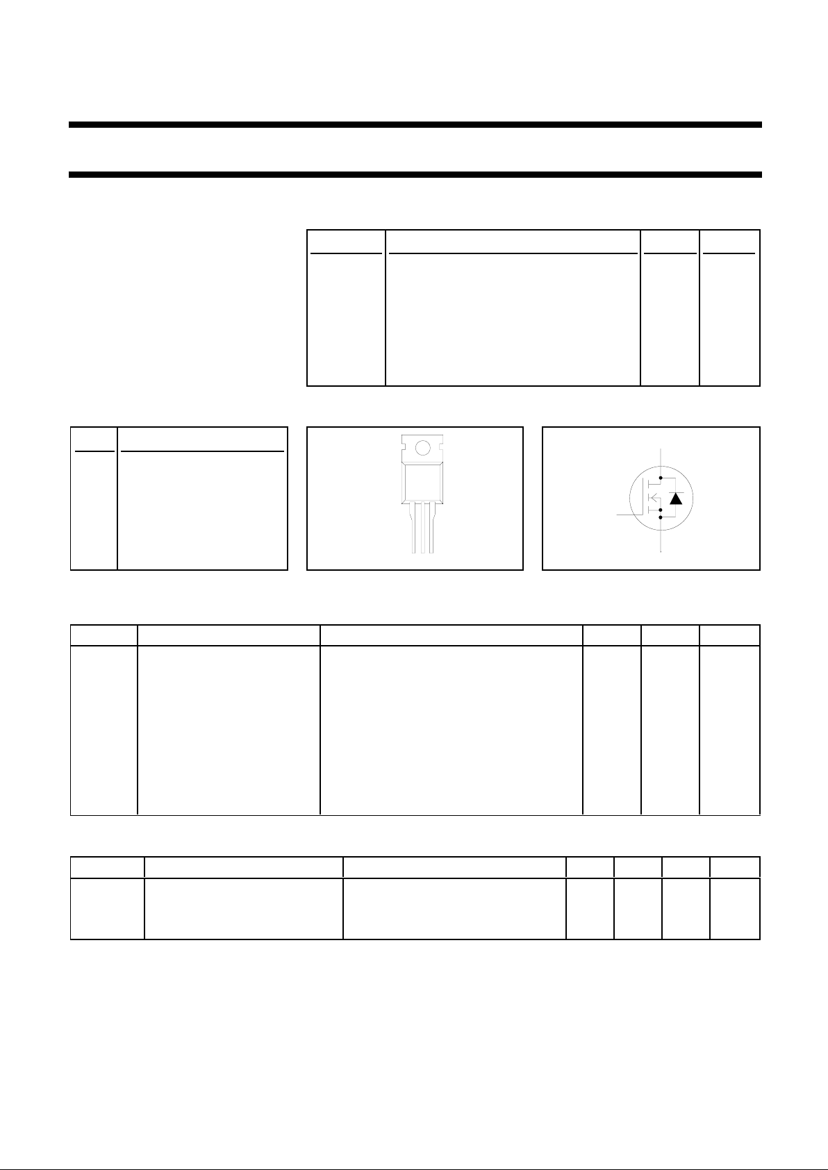
PowerMOS transistor PHP3055E
GENERAL DESCRIPTION QUICK REFERENCE DATA
N-channel enhancement mode SYMBOL PARAMETER MAX. UNIT
field-effect power transistor in a
plastic envelope featuring high V
DS
Drain-source voltage 60 V
avalanche energy capability, stable I
D
Drain current (DC) 12 A
blocking voltage, fast switching and P
tot
Total power dissipation 50 W
high thermal cycling performance R
DS(ON)
Drain-source on-state resistance 0.15 Ω
withlowthermalresistance.Intended
for use in Switched Mode Power
Supplies (SMPS), motor control
circuits and general purpose
switching applications.
PINNING - TO220AB PIN CONFIGURATION SYMBOL
PIN DESCRIPTION
1 gate
2 drain
3 source
tab drain
LIMITING VALUES
Limiting values in accordance with the Absolute Maximum System (IEC 134)
SYMBOL PARAMETER CONDITIONS MIN. MAX. UNIT
I
D
Continuous drain current Tmb = 25 ˚C; VGS = 10 V - 12 A
Tmb = 100 ˚C; VGS = 10 V - 9 A
I
DM
Pulsed drain current Tmb = 25 ˚C - 48 A
P
D
Total dissipation Tmb = 25 ˚C - 50 W
∆PD/∆TmbLinear derating factor Tmb > 25 ˚C - 0.33 W/K
V
GS
Gate-source voltage - ± 30 V
E
AS
Single pulse avalanche VDD ≤ 50 V; starting Tj = 25˚C; RGS = 50 Ω; - 25 mJ
energy VGS = 10 V
I
AS
Peak avalanche current VDD ≤ 50 V; starting Tj = 25˚C; RGS = 50 Ω;- 6 A
VGS = 10 V
Tj, T
stg
Operating junction and - 55 175 ˚C
storage temperature range
THERMAL RESISTANCES
SYMBOL PARAMETER CONDITIONS MIN. TYP. MAX. UNIT
R
th j-mb
Thermal resistance junction to - - 3 K/W
mounting base
R
th j-a
Thermal resistance junction to - 60 - K/W
ambient
123
tab
d
g
s
March 1997 1 Rev 1.000

Philips Semiconductors Product specification
PowerMOS transistor PHP3055E
ELECTRICAL CHARACTERISTICS
Tj = 25 ˚C unless otherwise specified
SYMBOL PARAMETER CONDITIONS MIN. TYP. MAX. UNIT
V
(BR)DSS
Drain-source breakdown VGS = 0 V; ID = 0.25 mA 60 - - V
voltage
∆V
(BR)DSS
/ Drain-source breakdown VDS = VGS; ID = 0.25 mA - 0.08 - V/K
∆T
j
voltage temperature coefficient
R
DS(ON)
Drain-source on resistance VGS = 10 V; ID = 6 A - 0.1 0.15 Ω
V
GS(TO)
Gate threshold voltage VDS = VGS; ID = 0.25 mA 2.0 3.0 4.0 V
g
fs
Forward transconductance VDS = 50 V; ID = 6 A 2.4 4.0 - S
I
DSS
Drain-source leakage current VDS = 60 V; VGS = 0 V - 0.1 25 µA
VDS = 48 V; VGS = 0 V; Tj = 150 ˚C - 1 250 µA
I
GSS
Gate-source leakage current VGS = ±30 V; VDS = 0 V - 10 100 nA
Q
g(tot)
Total gate charge ID = 10 A; V
DD
= 48 V; VGS = 10 V - 10 12 nC
Q
gs
Gate-source charge - 2 3 nC
Q
gd
Gate-drain (Miller) charge - 5.6 7 nC
t
d(on)
Turn-on delay time VDD = 30 V; ID = 10 A; - 8 - ns
t
r
Turn-on rise time RG = 24 Ω; RD = 2.7 Ω -55-ns
t
d(off)
Turn-off delay time - 25 - ns
t
f
Turn-off fall time - 22 - ns
L
d
Internal drain inductance Measured from contact screw on - 3.5 - nH
tab to centre of die
L
d
Internal drain inductance Measured from drain lead 6 mm - 4.5 - nH
from package to centre of die
L
s
Internal source inductance Measured from source lead 6 mm - 7.5 - nH
from package to source bond pad
C
iss
Input capacitance VGS = 0 V; VDS = 25 V; f = 1 MHz - 220 - pF
C
oss
Output capacitance - 108 - pF
C
rss
Feedback capacitance - 48 - pF
SOURCE-DRAIN DIODE RATINGS AND CHARACTERISTICS
Tj = 25 ˚C unless otherwise specified
SYMBOL PARAMETER CONDITIONS MIN. TYP. MAX. UNIT
I
S
Continuous source current Tmb = 25˚C - - 12 A
(body diode)
I
SM
Pulsed source current (body Tmb = 25˚C - - 48 A
diode)
V
SD
Diode forward voltage IS = 10 A; VGS = 0 V - - 1.5 V
t
rr
Reverse recovery time IS = 10 A; VGS = 0 V; - 38 - ns
dI/dt = 100 A/µs
Q
rr
Reverse recovery charge - 0.1 - µC
March 1997 2 Rev 1.000
Philips Semiconductors Product specification
PowerMOS transistor PHP3055E
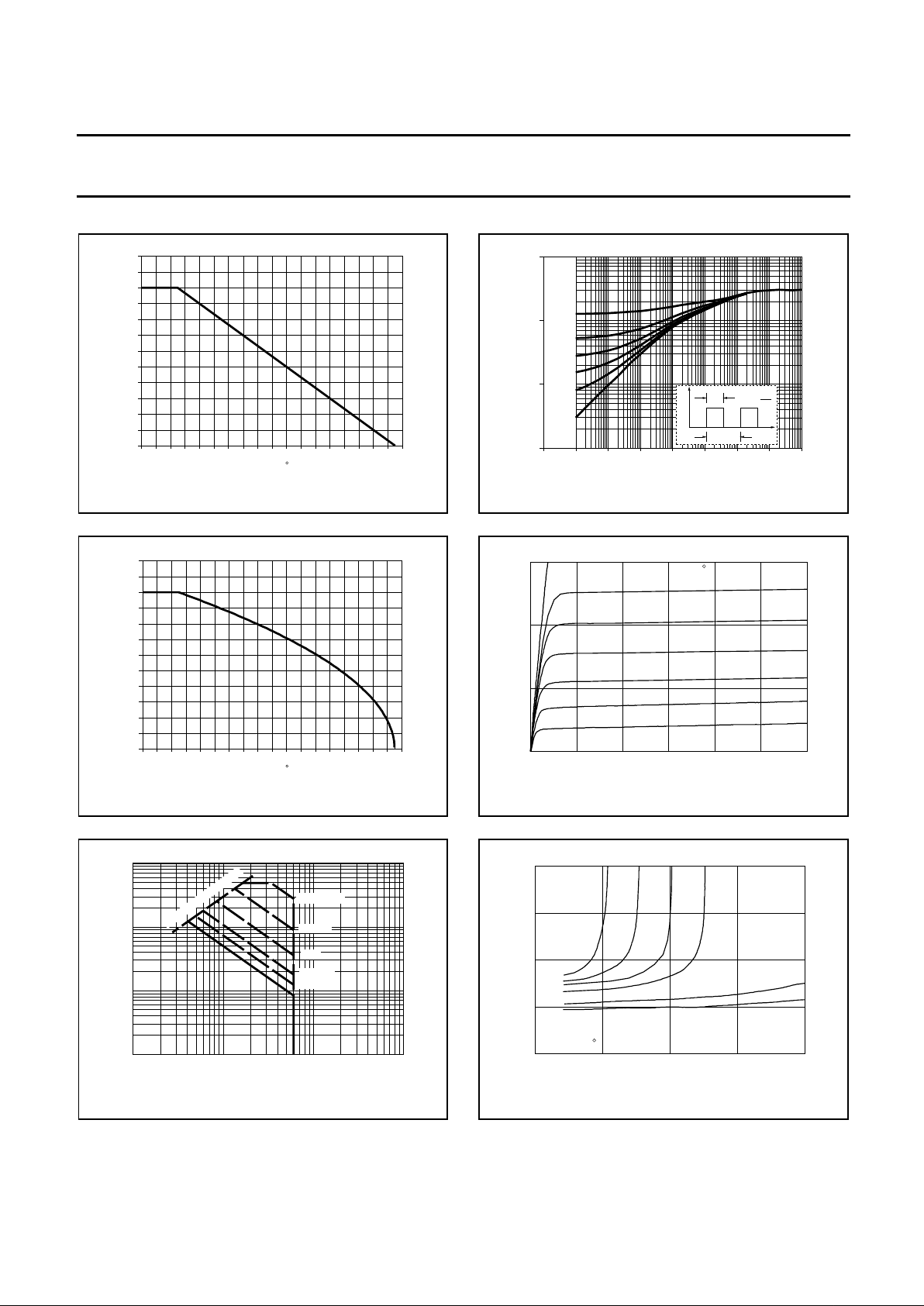
Fig.1. Normalised power dissipation.
PD% = 100⋅PD/P
D 25 ˚C
= f(Tmb)
Fig.2. Normalised continuous drain current.
ID% = 100⋅ID/I
D 25 ˚C
= f(Tmb); conditions: VGS ≥ 10 V
Fig.3. Safe operating area. Tmb = 25 ˚C
ID & IDM = f(VDS); IDM single pulse; parameter t
p
Fig.4. Transient thermal impedance.
Z
th j-mb
= f(t); parameter D = tp/T
Fig.5. Typical output characteristics
.
ID = f(VDS); parameter V
GS
Fig.6. Typical on-state resistance
.
R
DS(ON)
= f(ID); parameter V
GS
0 20 40 60 80 100 120 140 160 180
Tmb / C
PD%
Normalised Power Derating
120
110
100
90
80
70
60
50
40
30
20
10
0
0
0.5
0.2
0.1
0.05
0.02
D =
t
p
t
p
T
T
P
t
D
1us
10us 1ms
0.1s
10s
tp, pulse widtht (s)
Zth j-mb, Transient Thermal Impedance (K/W)
10
1
0.1
0.01
1s10ms100us
0 20 40 60 80 100 120 140 160 180
Tmb / C
ID%
Normalised Current Derating
120
110
100
90
80
70
60
50
40
30
20
10
0
0 5 10 15 20 25 30
0
5
10
15
PHP3055E
VDS, Drain-Source voltage (Volts)
ID, Drain current (Amps)
Tj = 25 C
VGS = 4.5 V
5 V
5.5 V
6 V
6.5 V
7 V
10 V
1 10 100 1000
0.1
1
10
100
DC
PHP3055E
VDS, Drain-source voltage (Volts)
ID, Drain current (Amps)
10 ms
100 ms
tp = 10 us
1 ms
100 us
RDS(ON) = VDS/ID
0 5 10 15 20
0
0.1
0.2
0.3
0.4
PHP3055E
ID, Drain current (Amps)
RDS(on), Drain-Source on resistance (Ohms)
VGS = 15 V
Tj = 25 C
10 V
7 V
6.5 V
6 V
5.5 V
March 1997 3 Rev 1.000
 Loading...