

Philips PN4416, PN4416A Datasheet

DISCRETE SEMICONDUCTORS
DATA SH EET
PN4416; PN4416A
N-channel field-effect transistor
Product specification
File under Discrete Semiconductors, SC07
December 1997
Philips Semiconductors Product specification
N-channel field-effect transistor PN4416; PN4416A
FEATURES
• Low noise
• Interchangeability of drain and
source connections
• High gain.
DESCRIPTION
N-channel symmetrical silicon
junction FETs in a SOT54 envelope.
These devices are intended for use in
VHF/UHF amplifiers, oscillators and
mixers.
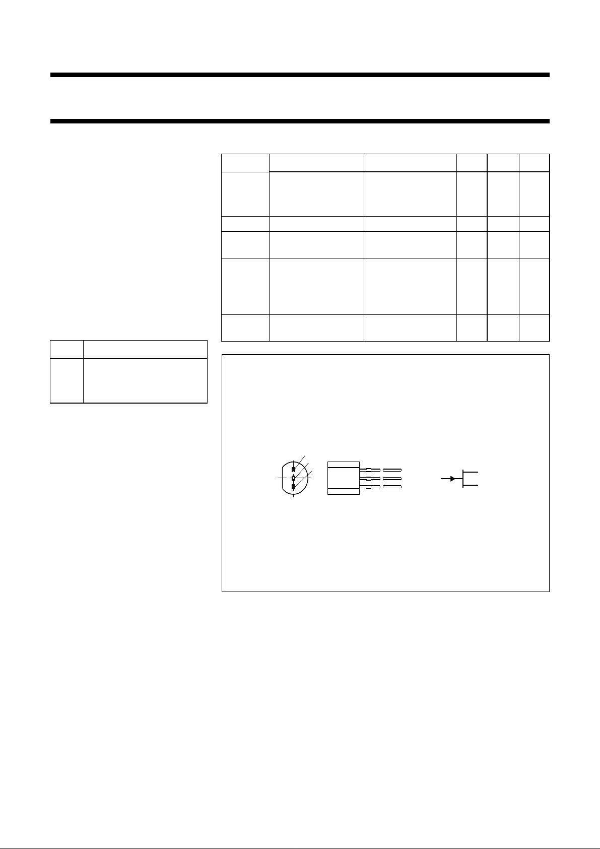
PINNING - SOT54 (TO-92).
PIN DESCRIPTION
1 gate
2 source
3 drain
QUICK REFERENCE DATA
SYMBOL PARAMETER CONDITIONS MIN. MAX. UNIT
V
DS
drain-source voltage
PN4416 − 30 V
PN4416A − 35 V
I
DSS
P
tot
drain current VDS = 15 V; VGS = 0 5 15 mA
total power
up to T
= 25 °C − 400 mW
amb
dissipation
V
GS(off)
gate-source cut-off
voltage
VDS = 15 V;
= 1 nA
I
D
PN4416 −−6V
PN4416A −2.5 −6V
Y
common-source
fs
transfer admittance
VDS = 15 V;
VGS = 0; f = 1 kHz
4.5 7.5 mS
handbook, halfpage
1
2
3
Fig.1 Simplified outline and symbol.
MAM042
g
d
s
December 1997 2

Philips Semiconductors Product specification
N-channel field-effect transistor PN4416; PN4416A
LIMITING VALUES
In accordance with the Absolute Maximum Rating System (IEC 134).
SYMBOL PARAMETER CONDITIONS MIN. MAX. UNIT
V
V
V
I
G
P
T
T
DS
GSO
GDO
tot
stg
j
drain-source voltage
PN4416 − 30 V
PN4416A − 35 V
gate-source voltage
PN4416 −−30 V
PN4416A −−35 V
gate-drain voltage
PN4416 −−30 V
PN4416A −−35 V
DC forward gate current − 10 mA
total power dissipation up to T
= 25 °C (note 1) − 400 mW
amb
storage temperature −65 +150 °C
junction temperature − 150 °C
THERMAL RESISTANCE
SYMBOL PARAMETER THERMAL RESISTANCE
R
th j-a
from junction to ambient (note 1) 350 K/W
Note
2
1. Mounted on a printed-circuit board, maximum lead length 4 mm, mounting pad for drain leads 10 mm
.
STATIC CHARACTERISTICS
= 25 °C unless otherwise specified.
T
j
SYMBOL PARAMETER CONDITIONS MIN. MAX. UNIT
V
(BR)GSS
gate-source breakdown voltage VDS = 0; IG = −1 µA
PN4416 −30 − V
PN4416A −35 − V
I
GSS
I
DSS
V
GSS
V
GS(off)
reverse gate leakage current VDS = 0; VGS = −15 V −−1nA
drain current VDS = 15 V; VGS = 0 5 15 mA
gate-source forward voltage VDS = 0; IG = 1 mA − 1V
gate-source cut-off voltage VDS = 15 V; ID = 1 nA
PN4416 −−6V
PN4416A −2.5 −6V
common source transfer admittance VDS = 15 V; VGS = 0 4.5 7.5 mS
Y
fs
common source output admittance VDS = 15 V; VGS = 0
Y
os
PN4416 − 50 µS
PN4416A − 50 µS
December 1997 3
 Loading...