

Philips PMV45EN User Manual

M3D088
1. Product profile
1.1 Description
1.2 Features
1.3 Applications
PMV45EN
µTrenchMOS™ enhanced logic level FET
Rev. 01 — 15 January 2003 Product data
N-channel enhancement mode field-effect transistor in a plastic package using
TrenchMOS™ technology.
Product availability:
PMV45EN in SOT23.
■ Surface mount package ■ Fast switching.
■ Battery management ■ High speed switch.
1.4 Quick reference data
■ VDS≤ 30 V ■ ID≤ 5.4 A
■ P
≤ 2W ■ R
tot
DSon
≤ 42 mΩ
2. Pinning information
Table 1: Pinning - SOT23 simplified outline and symbol
Pin Description Simplified outline Symbol
1 gate (g)
2 source (s)
3 drain (d)
12
Top view
3
MBB076
MSB003
SOT23
d
g
s

Philips Semiconductors
PMV45EN
µTrenchMOS™ enhanced logic level FET
3. Limiting values
Table 2: Limiting values
In accordance with the Absolute Maximum Rating System (IEC 60134).
Symbol Parameter Conditions Min Max Unit
V
DS
V
DGR
V
GS
I
D
I
DM
P
tot
T
stg
T
j
Source-drain diode
I
S
I
SM
drain-source voltage (DC) 25 °C ≤ Tj≤ 150 °C - 30 V
drain-gate voltage (DC) 25 °C ≤ Tj≤ 150 °C; RGS=20kΩ -30V
gate-source voltage (DC) - ±20 V
drain current (DC) Tsp=25°C; VGS=10V;Figure 2 and 3 - 5.4 A
= 100 °C; VGS=10V;Figure 2 - 3.4 A
T
sp
peak drain current Tsp=25°C; pulsed; tp≤ 10 µs; Figure 3 - 21.6 A
total power dissipation Tsp=25°C; Figure 1 -2W
storage temperature −55 +150 °C
junction temperature −55 +150 °C
source (diode forward) current (DC) Tsp=25°C - 1.7 A
peak source (diode forward) current Tsp=25°C; pulsed; tp≤ 10 µs - 6.9 A
9397 750 10894
Product data Rev. 01 — 15 January 2003 2 of 12
© Koninklijke Philips Electronics N.V. 2003. All rights reserved.
Philips Semiconductors
PMV45EN
µTrenchMOS™ enhanced logic level FET
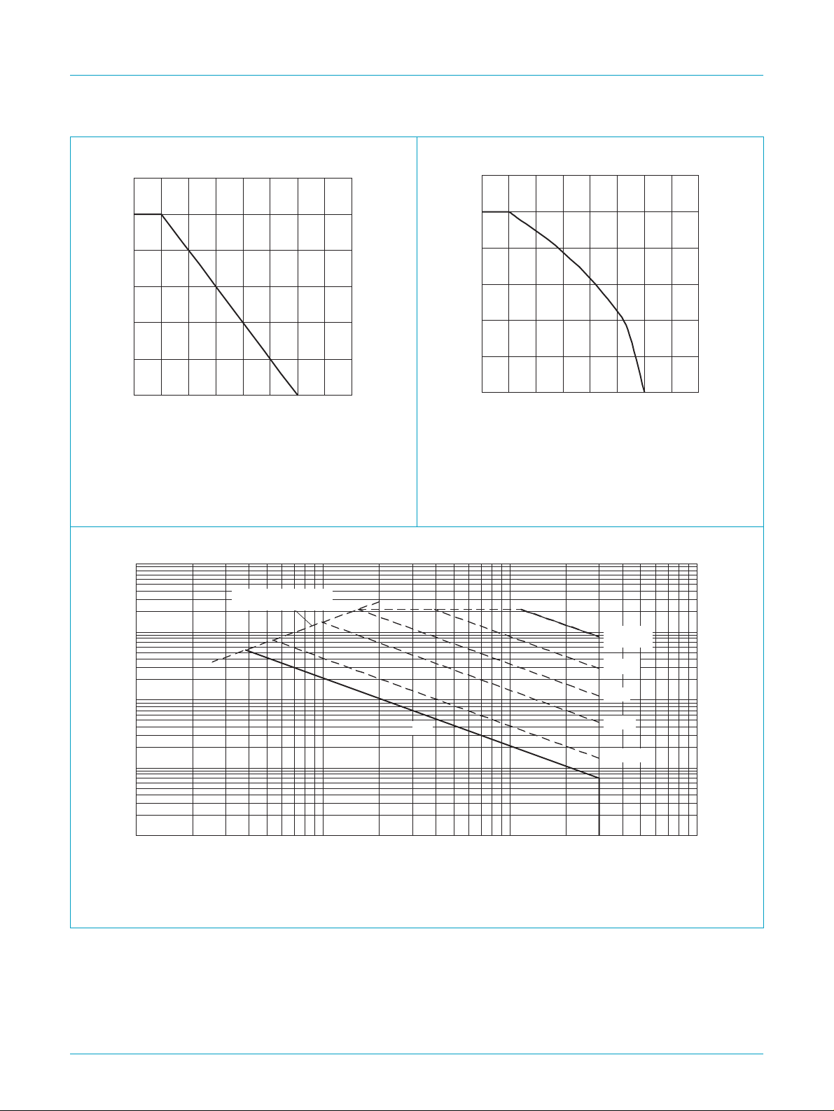
120
P
der
(%)
80
40
0
0 50 100 150 200
P
tot
P
der
-----------------------
P
tot 25 C°()
100%×= I
03aa17
Tsp (°C)
Fig 1. Normalized total power dissipation as a
function of solder point temperature.
2
10
I
D
(A)
Limit R
DSon
= VDS/I
D
120
I
der
(%)
80
40
0
0 50 100 150 200
I
D
der
-------------------
I
D25C
()
100%×=
°
03aa25
Tsp (°C)
Fig 2. Normalized continuous drain current as a
function of solder point temperature.
03al02
10
1
10
10
DC
-1
-2
-1
10
1 10 10
tp = 10 µs
100 µs
1 ms
10 ms
100 ms
VDS (V)
Tsp=25°C; IDMis single pulse; VGS=10V
Fig 3. Safe operating area; continuous and peak drain currents as a function of drain-source voltage.
2
9397 750 10894
© Koninklijke Philips Electronics N.V. 2003. All rights reserved.
Product data Rev. 01 — 15 January 2003 3 of 12
Philips Semiconductors
PMV45EN
µTrenchMOS™ enhanced logic level FET
4. Thermal characteristics
Table 3: Thermal characteristics
Symbol Parameter Conditions Min Typ Max Unit
R
th(j-sp)
thermal resistance from junction to solder point Figure 4 --60K/W
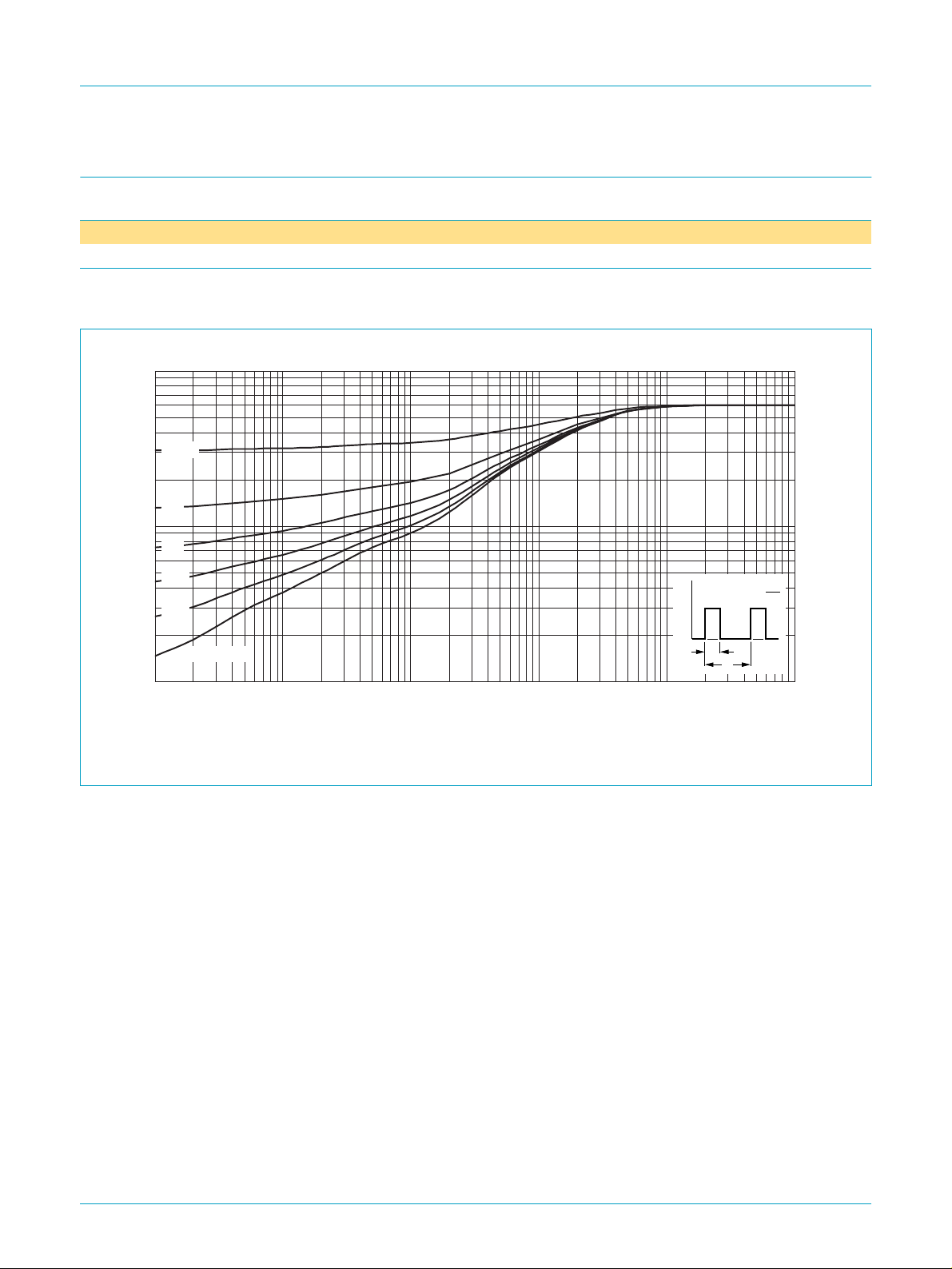
4.1 Transient thermal impedance
2
10
Z
th(j-sp)
(K/W)
10
1
= 0.5
δ
0.2
0.1
0.05
0.02
single pulse
-4
10
-3
10
-2
10
-1
10
P
t
p
T
1 10
tp (s)
Fig 4. Transient thermal impedance from junction to solder point as a function of pulse duration.
δ =
03ak68
t
p
T
t
9397 750 10894
© Koninklijke Philips Electronics N.V. 2003. All rights reserved.
Product data Rev. 01 — 15 January 2003 4 of 12
 Loading...