

Philips PLS159AA, PLS159AN Datasheet
Philips Semiconductors Programmable Logic Devices Product specification
PLS159A
Programmable logic sequencer
(16 × 45 × 12)
25
October 22, 1993 853–1159 11164
DESCRIPTION
The PLS159A is a 3-State output, registered
logic element combining AND/OR gate arrays
with clocked J-K flip-flops. These J-K
flip-flops are dynamically convertible to
D-type via a “fold-back” inverting buffer and
control gate F
C
. It features 8 registered I/O
outputs (F) in conjunction with 4 bidirectional
I/O lines (B). These yield variable I/O gate
and register configurations via control gates
(D, L) ranging from 16 inputs to 12 outputs.
The AND/OR arrays consist of 32 logic AND
gates, 13 control AND gates, and 21 OR
gates with fusible link connections for
programming I/O polarity and direction. All
AND gates are linked to 4 inputs (I),
bidirectional I/O lines (B), internal flip-flop
outputs (Q), and Complement Array output
(C
). The Complement Array consists of a
NOR gate optionally linked to all AND gates
for generating and propagating
complementary AND terms.
On-chip T/C buffers couple either True (I, B,
Q) or Complement (I
, B, Q, C) input polarities
to all AND gates, whose outputs can be
optionally linked to all OR gates. Any of the
32 AND gates can drive bidirectional I/O lines
(B), whose output polarity is individually
programmable through a set of Ex-OR gates
for implementing AND-OR or AND-NOR logic
functions. Similarly, any of the 32 AND gates
can drive the J-K inputs of all flip-flops. There
are 4 AND gates for the Asynchronous
Preset/Reset functions.
All flip-flops are positive edge-triggered and
can be used as input, output or I/O (for
interfacing with a bidirectional data bus) in
conjunction with load control gates (L),
steering inputs (I), (B), (Q) and
programmable output select lines (E).
The PLS159A is field-programmable,
enabling the user to quickly generate custom
patterns using standard programming
equipment.
FEATURES
•High-speed version of PLS159
•f
MAX
= 18MHz
– 25MHz clock rate
•Field-Programmable (Ni-Cr link)
•4 dedicated inputs
•13 control gates
•32 AND gates
•21 OR gates
•45 product terms:
– 32 logic terms
– 13 control terms
•4 bidirectional I/O lines
•8 bidirectional registers
•J-K, T, or D-type flip-flops
•Power-on reset feature on all flip-flops
(F
n
= 1)
•Asynchronous Preset/Reset
•Complement Array
•Active-High or -Low outputs
•Programmable OE control
•Positive edge-triggered clock
•Input loading: –100µA (max.)
•Power dissipation: 750mW (typ.)
•TTL compatible
•3-State outputs
APPLICATIONS
•Random sequential logic
•Synchronous up/down counters
•Shift registers
•Bidirectional data buffers
•Timing function generators
•System controllers/synchronizers
•Priority encoder/registers
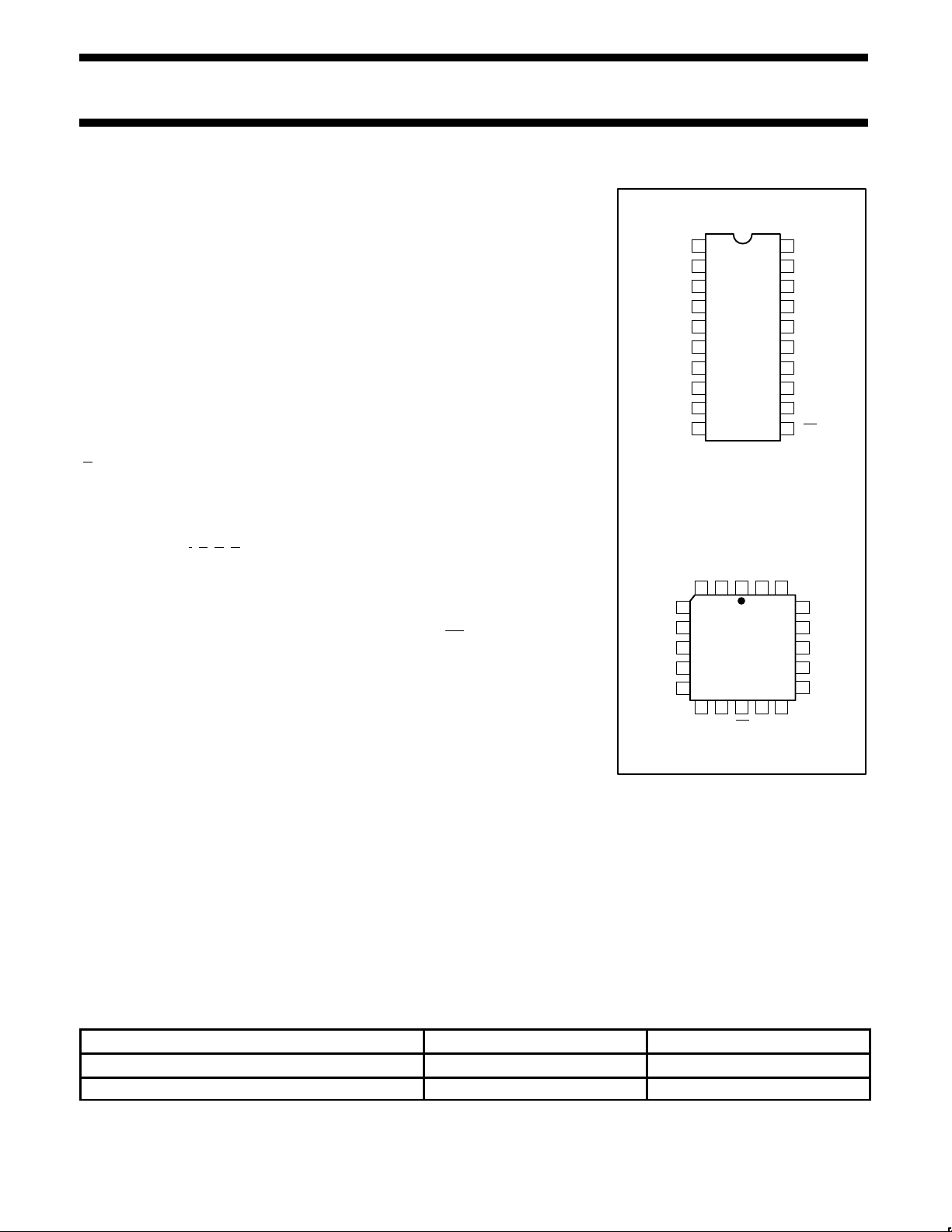
PIN CONFIGURATIONS
1
2
3
4
5
6
7
8
9
10 11
12
13
14
15
16
17
18
19
20
N Package
CLK
I0
I1
I2
I3
B0
B1
B2
B3 F0
GND
F1
F2
F3
F4
F5
F6
F7
V
CC
OE
123
4
5
6
7
8
9 10 11 12 13
14
15
16
17
18
1920
A Package
F0 F1
F2
F3
F4
F5
F6
F7
V
CC
OE
CLK
I0I1
I2
I3
B0
B1
B2
B3
GND
N = Plastic Dual In-Line Package (300mil-wide)
A = Plastic Leaded Chip Carrier
ORDERING INFORMATION
DESCRIPTION ORDER CODE DRAWING NUMBER
20-Pin Plastic Dual In-Line Package (300mil-wide) PLS159AN 0408D
20-Pin Plastic Leaded Chip Carrier PLS159AA 0400E
Philips Semiconductors Programmable Logic Devices Product specification
PLS159A
Programmable logic sequencer
(16 × 45 × 12)
October 22, 1993
26
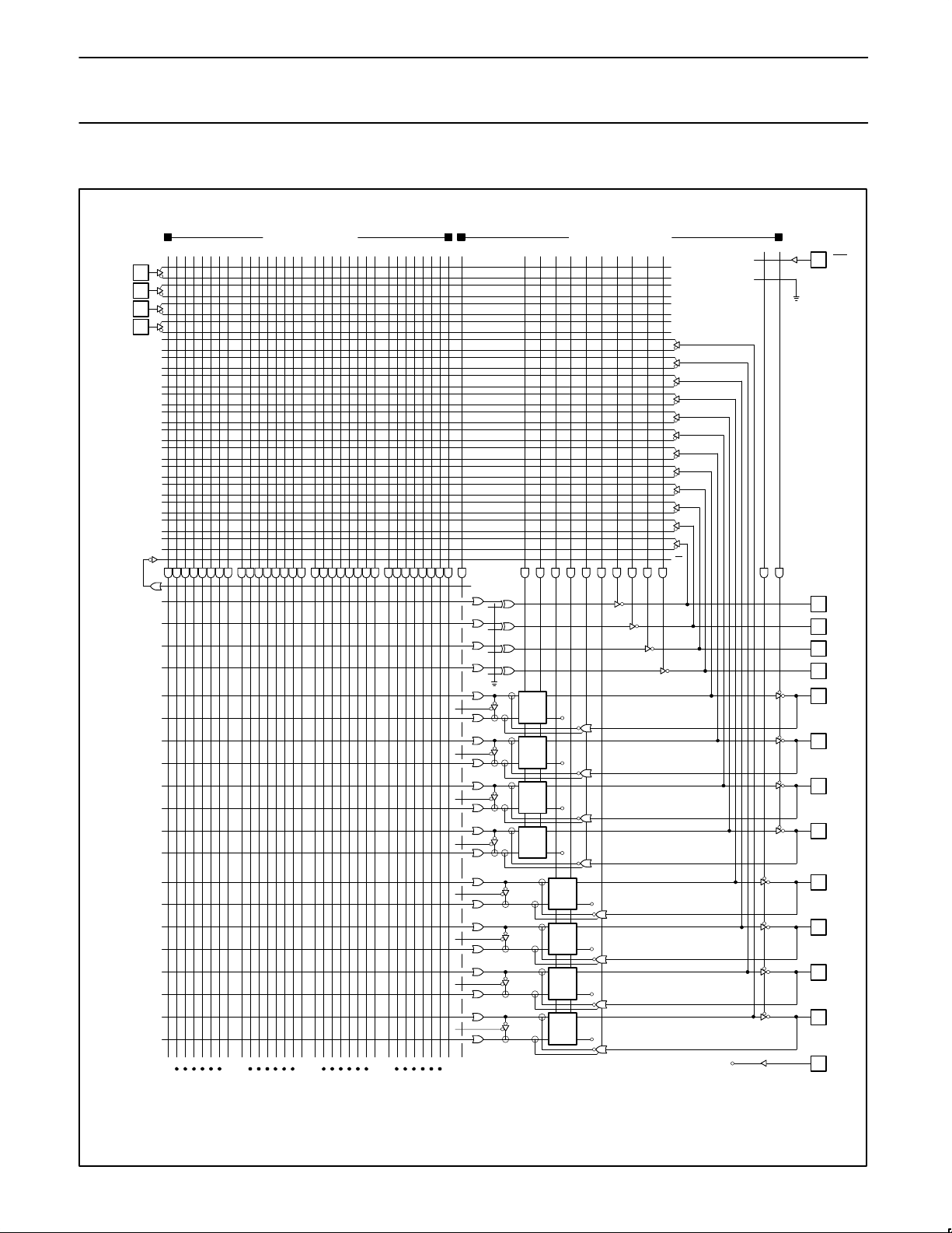
LOGIC DIAGRAM
(LOGIC TERMS-T) (CONTROL TERMS)
NOTES:
1. All OR gate inputs with a blown link float to logic “0”.
2. All other gates and control inputs with a blown link float to logic “1”.
3. ⊕ denotes WIRE-OR.
4. Programmable connection.
2
3
4
5
19
6
7
8
9
I0
I1
I2
I3
B3
B2
B1
B0
F7
31 24 23 16 15 8 7 0
P
BRBPARALBLA
D3 D2 D1 D0
X3
X2
X1
X0
B3
B2
B1
B0
F7
F6
F5
F4
F3
F2
C
C
F1
F0
S3
S2
S1
S0
J Q
K
EAE
B
CK’
18
F6
J Q
K
CK’
17
F5
J Q
K
CK’
16
F4
J Q
K
CK’
15
F3
J Q
K
CK’
14
F2
J Q
K
CK’
13
F1
J Q
K
CK’
12
F0
J Q
K
CK’
1
CLK
CK
F
C
11
OE
M7
M6
M5
M4
M3
M2
M1
M0
P R
P R

Philips Semiconductors Programmable Logic Devices Product specification
PLS159A
Programmable logic sequencer
(16 × 45 × 12)
October 22, 1993
27
FUNCTIONAL DIAGRAM
C
a
b
S
Q
Q
C
a
b
a
b
X
CK
P R
JKQ
M
(LOGIC TERMS) (CONTROL TERMS)
P
B
D
E
A
B
F
T
31
T0F
C
(4)
OE
E
B
CK
P R
JKQ
M
(4)
F
RBPAR
A
LBL
A
CLK
CK
0 1 0
0 0 1
STATE REGISTER
S
R
S
n + 1
PRESENT STATE
A
⋅ B ⋅ C ⋅ . . .
NEXT STATE
Q2 Q1 Q0
SET Q
0
: J0 = (Q
3
⋅ Q
2
⋅ Q1 ⋅ Q0) ⋅ A ⋅ B ⋅ C . . .
K
0
= 0
RESET Q
1
: J1 = 0
K
1
= (Q
3
⋅ Q
2
⋅ Q1 ⋅ Q0) ⋅ A ⋅ B ⋅ C . . .
HOLD Q
2
: J2 = 0
K
2
= 0
1
0
Q3
TOGGLE Q3: J3 = (Q
3
⋅ Q2 ⋅ Q1 ⋅ Q0) ⋅ A ⋅ B ⋅ C . . .
K3 = (Q
3
⋅ Q
2
⋅ Q1 ⋅ Q0) ⋅ A ⋅ B ⋅ C . . .
NOTE:
Similar logic functions are applicable for D
and T mode flip-flops.
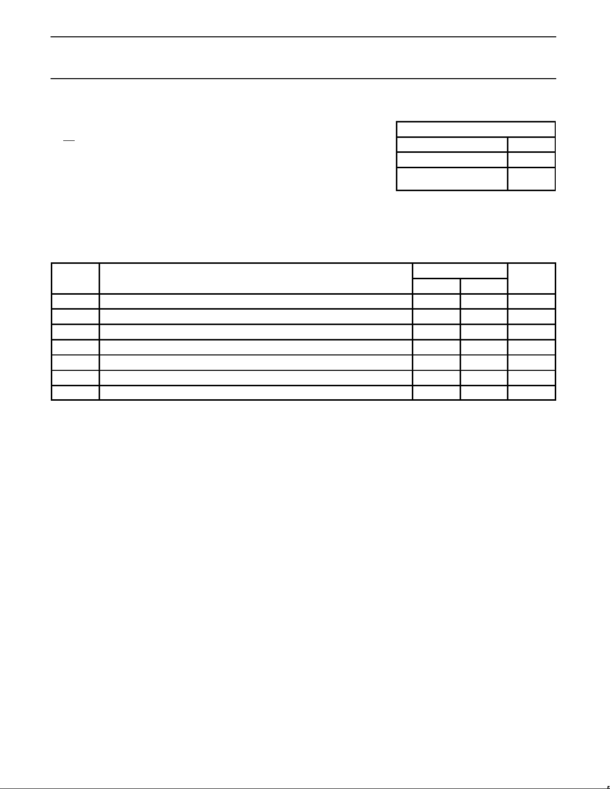
FLIP-FLOP TRUTH TABLE
OE L CK P R J K Q F
H Hi-Z
L X X L X X X L H
L X X H L X X H L
L X X L H X X L H
L L ↑ L L L L Q Q
L L ↑ L L L H L H
L L ↑ L L H L H L
L L ↑ L L H H Q Q
H H ↑ L L L H L H*
H H ↑ L L H L H L*
+10V X ↑ X X L H L H* *
X ↑ X X H L H L* *
NOTES:
1. Positive Logic:
J-K = T
0
+ T1 + T2 ……………… T
31
Tn = C⋅ (I0 ⋅ I1 ⋅ I2 …) ⋅ (Q0 ⋅ Q1 …) ⋅
(B0 ⋅ B1 ⋅ …)
2. ↑ denotes transition from Low to High level.
3. X = Don’t care
4. * = Forced at F
n
pin for loading the J-K
flip-flop in the Input mode. The load
control term, L
n
must be enabled (HIGH)
and the p-terms that are connected to the
associated flip-flop must be forced LOW
(disabled) during Preload.
5. At P = R = H, Q = H. The final state of Q
depends on which is released first.
6. * * = Forced at F
n
pin to load J-K flip-flop
independent of program code (Diagnostic
mode), 3-State B outputs.
LOGIC FUNCTION
Philips Semiconductors Programmable Logic Devices Product specification
PLS159A
Programmable logic sequencer
(16 × 45 × 12)
October 22, 1993
28
VIRGIN STATE
The factory shipped virgin device contains all
fusible links intact, such that:
1. OE
is always enabled.
2. Preset and Reset are always disabled.
3. All transition terms are disabled.
4. All flip-flops are in D-mode unless
otherwise programmed to J-K only or J-K
or D (controlled).
5. All B pins are inputs and all F pins are
outputs unless otherwise programmed.
CAUTION: PLS159A PROGRAMMING ALGORITHM
The programming voltage required to
program the PLS159A is higher (17.5V) than
that required to program the PLS159 (14.5V).
Consequently, the PLS159 programming
algorithm will not program the PLS159A.
Please exercise caution when accessing
programmer device codes to insure that the
correct algorithm is used.
THERMAL RATINGS
TEMPERATURE
Maximum junction 150°C
Maximum ambient 75°C
Allowable thermal rise
ambient to junction
75°C
ABSOLUTE MAXIMUM RATINGS
1
RATINGS
SYMBOL PARAMETER MIN MAX UNIT
V
CC
Supply voltage +7 V
DC
V
IN
Input voltage +5.5 V
DC
V
OUT
Output voltage +5.5 V
DC
I
IN
Input currents –30 +30 mA
I
OUT
Output currents +100 mA
T
amb
Operating temperature range 0 +75 °C
T
stg
Storage temperature range –65 +150 °C
NOTES:
1. Stresses above those listed may cause malfunction or permanent damage to the device. This is a stress rating only. Functional operation at
these or any other condition above those indicated in the operational and programming specification of the device is not implied.
 Loading...