


查询PDI1394P25供应商
INTEGRATED CIRCUITS
PDI1394P25
1-port 400 Mbps physical layer interface
Preliminary data
Supersedes data of 2001 Jul 18
2001 Sep 06
Philips Semiconductors Preliminary data
PDI1394P251-port 400 Mbps physical layer interface
1.0 FEATURES
•Fully supports provisions of IEEE 1394–1995 Standard for high
performance serial bus and the P1394a–2000 Standard
1
•Fully interoperable with Firewire and i.LINK implementations of
the IEEE 1394 Standard.
2
•Full P1394a support includes:
– Connection debounce
– Arbitrated short reset
– Multispeed concatenation
– Arbitration acceleration
– Fly-by concatenation
– Port disable/suspend/resume
•Provides one 1394a fully-compliant cable port at
100/200/400 Mbps. Can be used as a one port PHY without the
use of any extra external components
•Fully compliant with Open HCI requirements
•Cable ports monitor line conditions for active connection to remote
node.
•Power down features to conserve energy in battery-powered
applications include:
– Automatic device power down during suspend
– Device power down terminal
– Link interface disable via LPS
– Inactive ports powered-down
•Logic performs system initialization and arbitration functions
•Encode and decode functions included for data-strobe bit level
encoding
•Incoming data resynchronized to local clock
•Single 3.3 volt supply operation
•Minimum V
of 2.7 V for end-of-wire power-consuming devices
DD
•While unpowered and connected to the bus, will not drive TPBIAS
on a connected port, even if receiving incoming bias voltage on
that port
•Supports extended bias-handshake time for enhanced
interoperability with camcorders
•Interface to link-layer controller supports both low-cost bus-holder
isolation and optional Annex J electrical isolation
•Data interface to link-layer controller through 2/4/8 parallel lines at
49.152 MHz
•Low-cost 24.576 MHz crystal provides transmit, receive data at
100/200/400 Mbps, and link-layer controller clock at 49.152 MHz
•Does not require external filter capacitors for PLL
•Interoperable with link-layer controllers using 3.3 V and 5 V
supplies
•Interoperable with other Physical Layers (PHYs) using 3.3 V and
5 V supplies
•Node power class information signaling for system power
management
•Cable power presence monitoring
•Separate cable bias (TPBIAS) for each port
•Register bits give software control of contender bit, power class
bits, link active bit, and 1394a features
•LQFP package is function and pin compatible with the Texas
Instruments TSB41LV01E and TSB41AB1 (PAP package)
400 Mbps PHYs.
2.0 DESCRIPTION
The PDI1394P25 provides the digital and analog transceiver functions
needed to implement a one port node in a cable-based IEEE
1394–1995 and/or 1394a network. Each cable port incorporates two
differential line transceivers. The transceivers include circuitry to
monitor the line conditions as needed for determining connection
status, for initialization and arbitration, and for packet reception and
transmission. The PDI1394P25 is designed to interface with a Link
Layer Controller (LLC), such as the PDI1394L40 or PDI1394L41.
3.0 ORDERING INFORMATION
PACKAGE TEMPERATURE RANGE ORDER CODE PKG. DWG. #
64-pin plastic LQFP 0 to +70°C PDI1394P25BD SOT314-2
64-ball plastic LFBGA 0 to +70°C PDI1394P25EC SOT534-1
1. Implements technology covered by one or more patents of Apple Computer, Incorporated and SGS Thompson, Limited.
2. Firewire is a trademark of Apple Computer Inc. i.LINK is a trademark of Sony.
2001 Sep 06
2
Philips Semiconductors Preliminary data
PDI1394P251-port 400 Mbps physical layer interface
4.0 PIN AND BALL CONFIGURATION
4.1 LQFP CONFIGURA TION
LREQ
SYSCLK
CNA
CTL0
CTL1
PD
LPS
NC
DGND
1
2
3
4
5
D0
6
D1
7
D2
8
D3
9
D4
10
D5
11
12
D6
13
D7
14
15
16
DGND
DD
DGND
62 61 60 59 58 57 56 55 5464 63 53 52 51 50 49
19 20 21 22 23 24 25
DGND
DVDDDV
PC0
C/LKON
XOXIPLLGND
PC1
PC2
PLLGND
PDI1394P25
ISO
CPS
DD
PLLV
NCNCRESET
26 2717 18
DD
DD
DV
DV
DDAVDD
AV
28 29 30 31 32
DD
AV
TEST0
TESTM
BRIDGE
AGND
DD
AV
AGND
48
47
46
45
44
43
42
41
40
39
38
37
36
35
34
33 AGND
AGND
AGND
NC
NC
NC
NC
NC
AV
DD
R1
R0
AGND
TPBIAS0
TPA0+
TPA0–
TPB0+
TPB0–
2001 Sep 06
SV01828
3
Philips Semiconductors Preliminary data
PDI1394P251-port 400 Mbps physical layer interface
4.2 LFBGA CONFIGURA TION
BOTTOM (BALL) VIEW
ABCDEFGH
1
2
3
4
5
6
7
8
SV01909
Ball Signal Ball Signal Ball Signal Ball Signal
A1 AGND C1 RESET E1 PLLGND G1 DGND
A2 NC C2 AV
A3 NC C3 AV
DD
DD
E2 XI G2 DGND
E3 XO G3 CTL0
A4 R1 C4 NC E4 D2 G4 CTL1
A5 AGND C5 AV
DD
A6 TPBIAS0 C6 TPB0+ E6 DV
A7 TPB0– C7 AV
DD
E5 CPS G5 D5
DD
G6 PD
E7 PC1 G7 DGND
A8 AGND C8 TEST0 E8 ISO G8 DGND
B1 AGND D1 PLLV
B2 AGND D2 AV
DD
DD
F1 DV
F2 DV
DD
DD
H1 LREQ
H2 SYSCLK
B3 NC D3 PLLGND F3 CNA H3 D0
B4 NC D4 PLLV
DD
F4 D4 H4 D1
B5 TPA0+ D5 R0 F5 D6 H5 D3
B6 TPA0– D6 BRIDGE F6 C/LKON H6 D7
B7 AGND D7 TESTM F7 PC0 H7 LPS
B8 AV
DD
D8 DV
DD
F8 PC2 H8 DGND
2001 Sep 06
4
Philips Semiconductors Preliminary data
PDI1394P251-port 400 Mbps physical layer interface
5.0 PIN DESCRIPTION
Name Pin Type LQFP
AGND Supply 32, 33,
AV
DD
BRIDGE CMOS 28 D6 I BRIDGE input. This input is used to set the Bridge_Aware bits located in
C/LKON CMOS 5 V tol 19 F6 I/O Bus Manager Contender programming input and link-on output. On
CNA CMOS 3 F3 O Cable Not Active output. This terminal is asserted high when there are
CPS CMOS 24 E5 I Cable Power Status input. This terminal is normally connected to cable
CTL0,
CTL1
Supply 30, 31,
CMOS 5 V tol 4
Pin
Numbers
39, 48,
49, 50
42, 51,
52
5
LFBGA
Ball
Numbers
A1, A5,
A8, B1,
B2, B7
B8, C2,
C3, C5,
C7, D2
G3
G4
I/O Description
— Analog circuit ground terminals. These terminals should be tied together
to the low impedance circuit board ground plane.
— Analog circuit power terminals. A combination of high frequency
decoupling capacitors on each side are suggested, such as paralleled
0.1 µF and 0.001 µF. These supply terminals are separated from
PLLVDD and DVDD internal to the device to provide noise isolation. They
should be tied at a low impedance point on the circuit board.
the Vendor-Dependent register Page 7, base address 1001b, bit
positions 6 and 7. This pin is sampled during a hardware reset (RESET
low). When the BRIDGE pin is tied low (or through a 1 kΩ resistor to
accommodate other vendor’s pin-compatible chips), the Bridge_Aware
bits are set to “00” indicating a “non-bridge device.” When the BRIDGE
pin is tied high, the Bridge_Aware bits are set to “11” indicating a “1394.1
bridge compliant” device. The default setting of the Bridge_Aware bits
can be overridden by writing to the register. The Bridge_Aware bits are
reported in the self-ID packet at bit positions 18 and 19.
hardware reset, this terminal is used to set the default value of the
contender status indicated during self-ID. Programming is done by tying
the terminal through a 10-kΩ resistor to a high (contender) or low (not
contender). The resistor allows the link-on output to override the input.
If this pin is connected to a LLC driver pin for setting Bus Manager/IRM
contender status, then a 10-kΩ series resistor should be placed on this
line between the PHY and the LLC to prevent possible contention. In this
case. the pull-high or pull-low resistors mentioned in the previous
paragraph should not be used. Refer to Figure 9.
Following hardware reset, this terminal is the link-on output, which is
used to notify the LLC to power-up and become active. The link-on
output is a square-wave signal with a period of approximately 163 ns (8
SYSCLK cycles) when active. The link-on output is otherwise driven low,
except during hardware reset when it is high impedance.
The link-on output is activated if the LLC is inactive (LPS inactive or the
LCtrl bit cleared) and when:
a) the PHY receives a link-on PHY packet addressed to this node,
b) the PEI (port-event interrupt) register bit is 1, or
c) any of the CTOI (configuration-timeout interrupt), CPSI
(cable-power-status interrupt), or STOI (state-timeout interrupt)
register bits are 1 and the RPIE (resuming-port interrupt enable)
register bit is also 1.
Once activated, the link-on output will continue active until the LLC
becomes active (both LPS active and the LCtrl bit set). The PHY also
deasserts the link-on output when a bus-reset occurs unless the link-on
output would otherwise be active because one of the interrupt bits is set
(i.e., the link-on output is active due solely to the reception of a link-on
PHY packet).
NOTE: If an interrupt condition exists which would otherwise cause the
link-on output to be activated if the LLC were inactive, the link-on output
will be activated when the LLC subsequently becomes inactive.
no ports receiving incoming bias voltage.
power through a 390 kΩ resistor. This circuit drives an internal
comparator that is used to detect the presence of cable power.
I/O Control I/Os. These bi-directional signals control communication
between the PDI1394P25 and the LLC. Bus holders are built into
these terminals.
2001 Sep 06
5
Philips Semiconductors Preliminary data
PDI1394P251-port 400 Mbps physical layer interface
Name DescriptionI/OLFBGA
D0–D7 CMOS 5 V tol 6, 7, 8,
DGND Supply 17, 18,
DV
DD
ISO CMOS 23 E8 I Link interface isolation control input. This terminal controls the operation
LPS CMOS 5 V tol 15 H7 I Link Power Status input. This terminal is used to monitor the
LREQ CMOS 5 V tol 1 H1 I LLC Request input. The LLC uses this input to initiate a service request
NC No connect 54, 55 — These pins are not internally connected and consequently are “don’t
NC No connect 16, 43,
PC0
PC1
PC2
PD CMOS 5 V tol 14 G6 I Power Down input. A logic high on this terminal turns off all internal
Pin Type
Supply 25, 26,
CMOS 5 V tol 20
LQFP
Pin
Numbers
9, 10, 11,
12, 13
63, 64
61, 62
44, 45,
46, 47
21
22
Ball
Numbers
H3, H4,
E4, H5,
F4, G5,
F5, H6
G1, G2,
G7, G8,
H8
D8, E6,
F1, F2
A2, A3,
B3, B4,
C4
F7
E7
F8
I/O Data I/Os. These are bi-directional data signals between the
— Digital circuit ground terminals. These terminals should be tied together
— Digital circuit power terminals. A combination of high frequency
— No connect.
PDI1394P25 and the LLC. Bus holders are built into these terminals.
Unused Dn pins should be pulled to ground through 10 kΩ resistors.
to the low impedance circuit board ground plane.
decoupling capacitors near each side of the IC package are suggested,
such as paralleled 0.1 µF and 0.001 µF. Lower frequency 10 µF filtering
capacitors are also recommended. These supply terminals are
separated from PLLV
isolation. They should be tied at a low impedance point on the circuit
board.
of output differentiation logic on the CTL and D terminals. If an optional
isolation barrier of the type described in Annex J of IEEE Std 1394–1995
is implemented between the PDI1394P25 and LLC, the ISO terminal
should be tied low to enable the differentiation logic. If no isolation
barrier is implemented (direct connection), or bus holder isolation is
implemented, the ISO
differentiation logic.
active/power status of the link layer controller and to control the state of
the PHY -LLC interface. This terminal should be connected to either the
VDD supplying the LLC through a 10 kΩ resistor, or to a pulsed output
which is active when the LLC is powered. A pulsed signal should be
used when an isolation barrier exists between the LLC and PHY. (See
Figure 8)
The LPS input is considered inactive if it is sampled low by the PHY for
more than 2.6 µs (128 SYSCLK cycles), and is considered active
otherwise (i.e., asserted steady high or an oscillating signal with a low
time less than 2.6 µs). The LPS input must be high for at least 21 ns in
order to be guaranteed to be observed as high by the PHY.
When the PDI1394P25 detects that LPS is inactive, it will place the
PHY -LLC interface into a low-power reset state. In the reset state, the
CTL and D outputs are held in the logic zero state and the LREQ input is
ignored; however, the SYSCLK output remains active. If the LPS input
remains low for more than 26 µs (1280 SYSCLK cycles), the PHY-LLC
interface is put into a low-power disabled state in which the SYSCLK
output is also held inactive. The PHY -LLC interface is placed into the
disabled state upon hardware reset.
The LLC is considered active only if both the LPS input is active and the
LCtrl register bit is set to 1, and is considered inactive if either the LPS
input is inactive or the LCtrl register bit is cleared to 0.
to the PDI1394P25. Bus holder is built into this terminal.
cares”. Other vendors’ pin compatible chips may require
connections and external circuitry on these pins.
I Power Class programming inputs. On hardware reset, these inputs set
the default value of the power class indicated during self-ID.
Programming is done by tying the terminals high or low. Refer to
Table 21 for encoding.
circuitry except the cable-active monitor circuits which control the CNA
output. For more information, refer to Section 17.2
and AVDD internal to the device to provide noise
DD
terminal should be tied high to disable the
2001 Sep 06
6
Philips Semiconductors Preliminary data
gg
gg
PDI1394P251-port 400 Mbps physical layer interface
Name DescriptionI/OLFBGA
PLLGND Supply 57, 58 D3, E1 — PLL circuit ground terminals. These terminals should be tied together to
PLLV
DD
RESET CMOS 5 V tol 53 C1 I Logic reset input. Asserting this terminal low resets the internal logic. An
R0
R1
SYSCLK CMOS 2 H2 O System clock output. Provides a 49.152 MHz clock signal, synchronized
TEST0 CMOS 29 C8 I Test control input. This input is used in manufacturing tests of the
TESTM CMOS 27 D7 I Test control input. This input is used in manufacturing tests of the
TPA0+ Cable 37 B5 I/O
TPA0– Cable 36 B6 I/O
TPB0+ Cable 35 C6 I/O
TPB0– Cable 34 A7 I/O
TPBIAS0 Cable 38 A6 I/O Twisted-pair bias output. This provides the 1.86 V nominal bias voltage
XI
XO
Pin Type
Supply 56 D1, D4 — PLL circuit power terminals. A combination of high frequency decoupling
Bias 40
Crystal 59
LQFP
Pin
Numbers
41
60
Ball
Numbers
D5
A4
E2
E3
the low impedance circuit board ground plane.
capacitors near each terminal are suggested, such as paralleled 0.1 µF
and 0.001 µF. These supply terminals are separated from DVDD and
AVDD internal to the device to provide noise isolation. They should be
tied at a low impedance point on the circuit board.
internal pull-up resistor to VDD is provided so only an external
delay capacitor is required for proper power-up operation. For more
information, refer to Section 17.2. This input is otherwise a standard
Schmitt logic input, and can also be driven by an open-drain type driver.
— Current setting resistor pins These pins are connected to an external
resistance to set the internal operating currents and cable driver output
currents. A resistance of 6.34 kΩ ±1% is required to meet the IEEE
1394–1995 Std. output voltage limits.
with data transfers, to the LLC.
PDI1394P25. For normal use, this terminal should be tied to GND.
PDI1394P25. For normal use, this input may be tied to VDD (for
compatibility with other vendors’ pin-compatible PHY chips) or to PHY
GND (when a PDI1394P25 is an alternate device).
Twisted-pair cable A differential signal terminals. Board traces from each
pair of positive and negative differential signal terminals should be kept
matched and as short as possible to the external load resistors and to
the cable connector.
Twisted-pair cable B differential signal terminals. Board traces from each
pair of positive and negative differential signal terminals should be kept
matched and as short as possible to the external load resistors and to
the cable connector.
needed for proper operation of the twisted-pair cable drivers and
receivers, and for signaling to the remote nodes that there is an active
cable connection. These terminals must be decoupled with a
0.3 µF–1 µF capacitor to ground.
— Crystal oscillator inputs. These terminals connect to a 24.576 MHz
parallel resonant fundamental mode crystal. The optimum values for the
external shunt capacitors are dependent on the specifications of the
crystal used. Can also be driven by an external clock generator (leave
XO unconnected in this case and start supplying the external clock
before resetting the PDI1394P25). For more information, refer to
Section 17.5
2001 Sep 06
7
Philips Semiconductors Preliminary data
PDI1394P251-port 400 Mbps physical layer interface
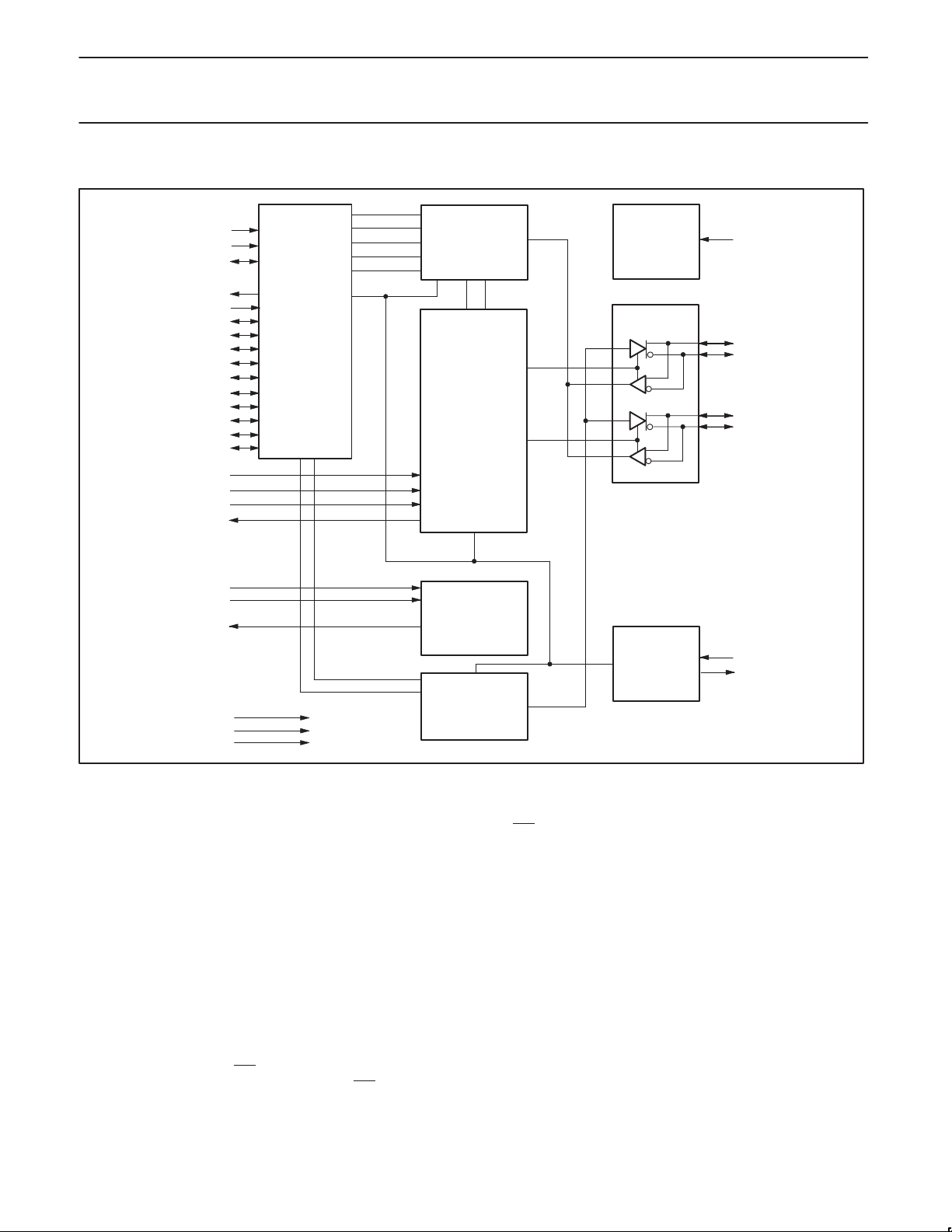
6.0 BLOCK DIAGRAM
LPS
/ISO
C/LKON
SYSCLK
LREQ
CTL0
CTL1
PC0
PC1
PC2
CNA
TPBIAS0
TESTM
/RESET
RECEIVED DATA
DECODER/
RETIMER
LINK
INTERFACE
D0
D1
D2
D3
D4
D5
D6
D7
R0
R1
PD
I/O
ARBITRATION
AND CONTROL
STATE MACHINE
LOGIC
BIAS VOLTAGE
AND
CURRENT
GENERATOR
TRANSMIT
DATA
ENCODER
CABLE POWER
DETECTOR
CABLE PORT 0
CRYSTAL
OSCILLATOR,
PLL SYSTEM,
AND CLOCK
GENERATOR
CPS
TPA0+
TPA0–
TPB0+
TPB0–
XI
XO
SV01829
7.0 FUNCTIONAL SPECIFICA TION
The PDI1394P25 requires only an external 24.576 MHz crystal as a
reference. An external clock can be connected to XI instead of a
crystal. An internal oscillator drives an internal phase-locked loop
(PLL), which generates the required 393.216 MHz reference signal.
This reference signal is internally divided to provide the clock signals
used to control transmission of the outbound encoded Strobe and
Data information. A 49.152 MHz clock signal, supplied to the
associated LLC for synchronization of the two chips, is used for
resynchronization of the received data. The Power Down (PD)
function, when enabled by asserting the PD terminal high, stops
operation of the PLL and disables all circuits except the cable bias
detectors at the TPB terminals. The port transmitter circuitry and the
receiver circuitry are also disabled when the port is disabled,
suspended, or disconnected.
The PDI1394P25 supports an optional isolation barrier between
itself and its LLC. When the ISO
LLC interface outputs behave normally. When the ISO
tied low, internal differentiating logic is enabled, and the outputs are
driven such that they can be coupled through a capacitive or
transformer galvanic isolation barrier as described in
section 5.9.4
. To operate with single capacitor (bus holder) isolation,
2001 Sep 06
input terminal is tied high, the
terminal is
IEEE 1394a
the ISO
on the PHY terminal must be tied high. For more details on
using single capacitor isolation, please refer to the Philips Isolation
Application Note AN2452.
Data bits to be transmitted through the cable ports are received from
the LLC on two, four or eight parallel paths (depending on the
requested transmission speed). They are latched internally in the
PDI1394P25 in synchronization with the 49.152 MHz system clock.
These bits are combined serially, encoded, and transmitted at
98.304/196.608/393.216 Mbps (referred to as S100, S200, and
S400 speed, respectively) as the outbound data-strobe information
stream. During transmission, the encoded data information is
transmitted differentially on the TPB cable pair(s), and the encoded
strobe information is transmitted differentially on the TP A cable
pair(s).
During packet reception the TPA and TPB transmitters of the
receiving cable port are disabled, and the receivers for that port are
enabled. The encoded data information is received on the TPA cable
pair, and the encoded strobe information is received on the TPB
cable pair. The received data-strobe information is decoded to
recover the receive clock signal and the serial data bits. The serial
8

Philips Semiconductors Preliminary data
PDI1394P251-port 400 Mbps physical layer interface
data bits are split into two-, four- or eight-bit parallel streams
(depending upon the indicated receive speed), resynchronized to
the local 49.152 MHz system clock and sent to the associated LLC.
Both the TPA and TPB cable interfaces incorporate dif ferential
comparators to monitor the line states during initialization and
arbitration. The outputs of these comparators are used by the
internal logic to determine the arbitration status. The TPA channel
monitors the incoming cable common-mode voltage. The value of
this common-mode voltage is used during arbitration to set the
speed of the next packet transmission (speed signaling). In addition,
the TPB channel monitors the incoming cable common-mode
voltage on the TPB pair for the presence of the remotely supplied
twisted-pair bias voltage (cable bias detection).
The PDI1394P25 provides a 1.86 V nominal bias voltage at the
TPBIAS terminal for port termination. The PHY contains two
independent TPBIAS circuits. This bias voltage, when seen through
a cable by a remote receiver, indicates the presence of an active
connection. This bias voltage source must be stabilized by an
external filter capacitor of 0.3 µF–1 µF.
The line drivers in the PDI1394P25 operate in a high-impedance
current mode, and are designed to work with external 112 Ω
line-termination resistor networks in order to match the 110 Ω cable
impedance. One network is provided at each end of all twisted-pair
cable connections. Each network is composed of a pair of
series-connected 56 Ω resistors. The midpoint of the pair of resistors
that is directly connected to the twisted-pair A terminals is connected
to its corresponding TPBIAS voltage terminal. The midpoint of the pair
of resistors that is directly connected to the twisted-pair B terminals is
coupled to ground through a parallel R-C network with recommended
values of 5 kΩ and 220 pF. The values of the external line termination
resistors are designed to meet the standard specifications when
connected in parallel with the internal receiver circuits. An external
resistor connected between the R0 and R1 terminals sets the driver
output current, along with other internal operating currents. This
current setting resistor has a value of 6.34 kΩ ±1%.
When the power supply of the PDI1394P25 is removed while the
twisted-pair cables are connected, the PDI1394P25 transmitter and
receiver circuitry presents a high impedance to the cable in order to
not load the TPBIAS voltage on the other end of the cable.
The TEST0 terminal is used to set up various manufacturing test
conditions. For normal operation, it should be connected to ground.
The TESTM terminal is used in manufacturing tests of the
PDI1394P25. For normal use, it may be tied to either PHY V
compatability with other vendors’ pin-compatible PHY chips) or to
PHY GND (when a PDI1394P25 is an alternate device).
The BRIDGE terminal is used to set the default value of the
Bridge_Aware bits i the Page 7 (Vendor Dependent) register. Tying
BRIDGE low directly (or through a 1 kΩ resistor to accommodate
other vendors’ pin-compatible chips), defaults the Bridge_Aware
field to “00” indicating a “non-bridge device.” Tying BRIDGE high,
defaults the Bridge_Aware bit to “11” indicating a “1394.1 bridge
compliant” device. Writing to the Bridge_Aware field overrides the
default setting from the BRIDGE terminal. The Bridge_Aware field is
reported in the self-ID packet at bit positions 18 and 19.
DD
(for
Four package terminals, used as inputs to set the default value for
four configuration status bits in the self-ID packet, should be
hard-wired high or low as a function of the equipment design. The
PC0–PC2 terminals are used to indicate the default power-class
status for the node (the need for power from the cable or the ability
to supply power to the cable). See Table 21 for power class
encoding. The C/LKON terminal is used as an input to indicate that
the node is a contender for bus manager.
The PHY supports suspend/resume as defined in the IEEE 1394a
specification. The suspend mechanism allows pairs of directly
connected ports to be placed into a low power state while
maintaining a port-to-port connection between 1394 bus segments.
While in a low power state, a port is unable to transmit or receive
data transaction packets. However, a port in a low power state is
capable of detecting connection status changes and detecting
incoming TPBIAS. When the PDI1394P25’s port is suspended, all
circuits except the bias-detection circuits are powered down,
resulting in significant power savings. The TPBIAS circuit monitors
the value of incoming TPA pair common-mode voltage when local
TPBIAS is inactive. Because this circuit has an internal current
source and the connected node has a current sink, the monitored
value indicates the cable connection status. This monitor is called
connect-detect.
Both the cable bias-detect monitor and TPBIAS connect-detect
monitor are used in suspend/resume signaling and cable connection
detection. For additional details of suspend/resume operation, refer
to the 1394a specification. The use of suspend/resume is
recommended for new designs.
The port transmitter and receiver circuitry is disabled during power
down (when the PD input terminal is asserted high), during reset
(when the RESET
cable is connected to the port, or when controlled by the internal
arbitration logic. The port twisted-pair bias voltage circuitry is
disabled during power down, during reset, or when the port is
disabled as commanded by the LLC.
The CNA (cable-not-active) terminal provides a high when the
twisted-pair cable port is not receiving incoming bias (i.e., it is either
disconnected or suspended), and can be used along with LPS to
determine when to power-down the PDI1394P25. The CNA output is
not debounced. When the PD terminal is asserted high, the CNA
detection circuitry is enabled (regardless of the previous state of the
ports) and a pull-down is activated on the RESET
force a reset of the PDI1394P25 internal logic.
The LPS (link power status) terminal works with the C/LKON
terminal to manage the power usage in the node. The LPS signal
from the LLC is used in conjunction with the LCtrl bit (see Table 1
and Table 2) to indicate the active/power status of the LLC. The LPS
signal is also used to reset, disable, and initialize the PHY -LLC
interface (the state of the PHY -LCC interface is controlled solely by
the LPS input regardless of the state of the LCtrl bit).
input terminal is asserted low), when no active
terminal so as to
2001 Sep 06
9
Philips Semiconductors Preliminary data
SYMBOL
PARAMETER
CONDITION
UNIT
Electrostatic discharge
PDI1394P251-port 400 Mbps physical layer interface
The LPS input is considered inactive if it remains low for more than
2.6 µs and is considered active otherwise. When the PDI1394P25
detects that LPS is inactive, it will place the PHY -LLC interface into a
low-power reset state in which the CTL and D outputs are held in the
logic zero state and the LREQ input is ignored; however, the
SYSCLK output remains active. If the LPS input remains low for
more than 26 µs, the PHY-LLC interface is put into a low-power
disabled state in which the SYSCLK output is also held inactive. The
PHY -LLC interface is also held in the disabled state during hardware
reset. The PDI1394P25 will continue the necessary repeater
functions required for normal network operation regardless of the
state of the PHY -LLC interface. When the interface is in the reset or
disabled state and LPS is again observed active, the PHY will
initialize the interface and return it to normal operation.
8.0 ABSOLUTE MAXIMUM RATINGS
In accordance with the Absolute Maximum Rating System (IEC 134). Voltages are referenced to GND (ground = 0 V).
V
VI–5 V 5 volt tolerant input voltage range –0.5 5.5 V
V
T
amb
T
NOTE:
1. Stresses beyond those listed under “Absolute Maximum Ratings” may cause permanent damage to the device. These are stress ratings
only, and functional operation of the device at these or any other conditions beyond those indicated under “Recommended Operating
Conditions” is not implied. Exposure to absolute-maximum-rated conditions for extended periods may affect device reliability .
DC supply voltage –0.5 4.0 V
DD
V
DC input voltage –0.5 VDD+0.5 V
I
DC output voltage range at any output –0.5 VDD+0.5 V
O
Operating free-air temperature range 0 +70 °C
Storage temperature range –65 +150 °C
stg
1
The PHY uses the C/LKON terminal to notify the LLC to power up
and become active. When activated, the C/LKON signal is a square
wave of approximately 163 ns period. The PHY activates the
C/LKON output when the LLC is inactive and a wake-up event
occurs. The LLC is considered inactive when either the LPS input is
inactive, as described above, or the LCtrI bit is cleared to 0. A
wake-up event occurs when a link-on PHY packet addressed to this
node is received, or conditionally when a PHY interrupt occurs. The
PHY deasserts the C/LKON output when the LLC becomes active
(both LPS active and the LCtrl bit set to 1). The PHY also deasserts
the C/LKON output when a bus-reset occurs unless a PHY interrupt
condition exists which would otherwise cause C/LKON to be active.
LIMITS
MIN MAX
Human Body Model — 2 kV
Machine Model — 200 V
2001 Sep 06
10
Philips Semiconductors Preliminary data
SYMBOL
PARAMETER
CONDITION
MIN
TYP
MAX
UNIT
VDDSu ly voltage
gg
VIDDifferential in ut voltage am litude
V
TPB common-mode in ut voltage
gg
V
TPB common-mode in ut voltage
S200 s eed signal
V
TPB common-mode in ut voltage
S400 s eed signal
PDI1394P251-port 400 Mbps physical layer interface
9.0 RECOMMENDED OPERATING CONDITIONS
pp
High-level input voltage, LREQ,
CTL0, CTL1, D0-D7
V
IH
High-level input voltage, C/LKON2,
Source power node 3.0 3.3 3.6 V
Non-source power node 2.7
ISO = VDD, VDD >= 2.7 V 2.3 — — V
ISO = VDD, VDD >= 3.0 V 2.6 — — V
PC0–PC2, ISO, PD
RESET 0.6 V
Low-level input voltage, LREQ,
CTL0, CTL1, D0–D7
V
Low-level input voltage, C/LKON2,
IL
PC0–PC2, ISO, PD,
ISO = V
DD
RESET — — 0.3 V
I
Output current TPBIAS outputs –6 — 2.5 mA
O
TPA, TPB cable inputs, during data reception 118 — 260 mV
TPA, TPB cable inputs, during data arbitration 168 — 265 mV
Speed signaling off
or S100 speed signal
p
p
Source power node 1.165 — 2.515 V
Non-source power node 1.165 — 2.015
Source power node 0.935 — 2.515 V
Non-source power node 0.935 — 2.015
Source power node 0.523 — 2.515 V
Non-source power node 0.523 — 2.015
IC-100
IC-200
IC-400
t
PU
p
p
p
p
p
Power-up reset time Set by capacitor between RESET pin and GND 2 — — ms
TPA, TPB cable inputs, S100 operation — — 1.08 ns
Receive input jitter
TPA, TPB cable inputs, S200 operation — — 0.5 ns
TPA, TPB cable inputs, S400 operation — — 0.315 ns
Between TPA and TPB cable inputs, S100 operation — — 0.8 ns
Receive input skew
Between TPA and TPB cable inputs, S200 operation — — 0.55 ns
Between TPA and TPB cable inputs, S400 operation — — 0.5 ns
f
XTAL
Crystal or external clock frequency
Crystal connected according to Figure 10 or external
clock input at pin XI
NOTES:
1. For a node that does not source power to the bus (see Section 4.2.2.2 in the IEEE 1394-1995 standard).
2. C/LKON is only an input when RESET
= 0.
1
3.0 3.6 V
0.7 V
— — V
DD
— —
DD
— — 0.7 V
— — 0.2 V
DD
DD
V
—
1
V
1
V
1
V
24.5735 24.576 24.5785 MHz
2001 Sep 06
11
Philips Semiconductors Preliminary data
SYMBOL
PARAMETER
TEST CONDITION
UNIT
I
gg , ,
SYMBOL
PARAMETER
TEST CONDITION
UNIT
ZIDDifferential input impedance
Drivers disabled
ZICCommon mode input impedance
Drivers disabled
PDI1394P251-port 400 Mbps physical layer interface
10.0 CABLE DRIVER
LIMITS
MIN TYP MAX
V
I
O(diff)
V
NOTES:
1. Limits defined as algebraic sum of TP A+ and TPA– driver currents. Limits also apply to TPB+ and TPB– algebraic sum of driver currents.
2. Limits defined as one half of the algebraic sum of currents flowing out of TPB+ and TPB–.
11.0 CABLE RECEIVER
V
V
V
V
V
TH–SP200
V
TH–SP400
Differential output voltage 56 Ω load 172 — 265 mV
OD
Drivers enabled,
Driver Difference current, TP A+, TPA–, TPB+, TPB–
Common mode speed signaling output current, TPB+,
SP
OFF
2
TPB–
OFF state differential voltage Drivers disabled — — 20 mV
1
speed signaling OFF
–0.88 — 0.88 mA
200 Mbps speed signaling enabled –4.84 — –2.53 mA
400 Mbps speed signaling enabled –12.4 — –8.10 mA
LIMITS
MIN TYP MAX
10 14 —
— — 4 pF
20 — — kΩ
— — 24 pF
49 — 131 mV
314 — 396 mV
TH-R
TH-CB
TH+
TH–
I
CD
p
p
p
p
Receiver input threshold voltage Drivers disabled –30 — 30 mV
Cable bias detect threshold, TPBn cable inputs Drivers disabled 0.6 — 1.0 V
Positive arbitration comparator input threshold
voltage
Negative arbitration comparator input threshold
voltage
Speed signal input threshold
Speed signal input threshold
Drivers disabled 89 — 168 mV
Drivers disabled –168 — –89 mV
TPBIAS–TPA common mode voltage,
drivers disabled 200 Mbps
TPBIAS–TPA common mode voltage,
drivers disabled 400 Mbps
Connect detect output at TPBIAS pins Drivers disabled — — –76 µA
kΩ
2001 Sep 06
12
Philips Semiconductors Preliminary data
CTL1, D0 D7, SYSCLK, CNA
V
g, ,
VOHHigh-level output voltage, pin C/LKON
PDI1394P251-port 400 Mbps physical layer interface
12.0 OTHER DEVICE I/O
SYMBOL PARAMETER TEST CONDITION MIN TYP MAX UNIT
See Note 1 — 56 — mA
I
DD
I
DD–PD
V
TH
V
OH
OL
V
OL
I
BH+
I
BH–
I
I
I
OZ
I
RST-UP
I
RST-DN
V
IT+
V
IT–
V
LIT+
V
LIT–
V
O
Supply current
Supply current in power down mode PD = VDD in power down mode — 150 — µA
Cable power status threshold voltage
High-level output voltage, pins CTL0,
–
Low-level output voltage, pins CTL0,
CTL1, D0–D7, CNA, SYSCLK
p
p
Low-level output voltage, pin C/LKON VDD = 2.7 V, IOL = 4 mA; See Note 4 — — 0.3 V
Positive peak bus holder current, pins
CTL0, CTL1, D0–D7, LREQ
Negative peak bus holder current, pins
CTL0, CTL1, D0–D7, LREQ
Input current, pins LREQ, LPS, PD,
TEST0, BRIDGE, PC0–PC2
Off-state current, pins CTL0, CTL1,
D0–D7, C/LKON
Pullup current, RESET input VI = 1.5 V or 0 V –90 — –20 µA
Pulldown current, RESET input VI = VDD, PD = V
Positive going threshold voltage, LREQ,
CTL0, CTL1, D0–D7, C/LKON inputs
Negative going threshold voltage, LREQ,
CTL0, CTL1, D0–D7, C/LKON inputs
Positive going threshold voltage, LPS
inputs
Negative going threshold voltage, LPS
inputs
TPBIAS output voltage At rated IO current 1.665 — 2.015 V
NOTES:
1. Transmit Max Packet (1 port transmitting max size isochronous packet (4096 bytes), sent on every isochronous interval, S400, data value of
0xCCCCCCCCh), V
2. Receive typical packet (1 port receiving DV packets on every isochronous interval, S100), V
3. Idle (1 Port transmitting cycle starts) V
4. The C/LKON pin is able to drive an isolation circuit according to Figure 5A-20 of the IEEE-1394a-2000 standard.
= 3.3 V, TA = 25 °C
DD
= 3.3 V, TA = 25 °C
DD
See Note 2 — 40 — mA
See Note 3 — 38 — mA
390 kΩ resistor between cable power
and CPS pin: Measured at cable power
4.7 — 7.5 V
side of resistor
VDD >= 2.7 V , IOH = –4 mA, ISO = V
VDD >= 3.0 V , IOH = –4 mA, ISO = V
DD
DD
2.4 — — V
2.8 — — V
Annex J: IOH = –9 mA, ISO = 0 VDD–0.4 — — V
IOL = 4 mA, ISO = V
DD
— — 0.4 V
Annex J: IOL = 9 mA, ISO = 0 — — 0.4 V
VDD = 2.7 V, IOH = –4 mA ; See Note 4 2.4 — — V
VDD >= 3.0 V , IOH = –4 mA ; See Note 4 2.7 — — V
ISO = VDD, VI = 0 V to V
ISO = VDD, VI = 0 V to V
DD
DD
0.05 — 1.0 mA
–1.0 — –0.05 mA
ISO = 0 V; VDD = 3.6 V — — 5 µA
VO = VDD or 0 V –5 — 5 µA
DD
.4 1.6 2.8 mA
ISO = 0 V VDD/2 + 0.3 — VDD/2 + 0.9 V
ISO = 0 V VDD/2 – 0.9 — VDD/2 – 0.3 V
V
V
LREF
LREF
= 0.42 x V
= 0.42 x V
DD
DD
— — V
V
+0.2 — — V
LREF
= 3.3 V, TA = 25 °C
DD
LREF
+1 V
2001 Sep 06
13
Philips Semiconductors Preliminary data
SYMBOL
PARAMETER
TEST CONDITION
UNIT
PDI1394P251-port 400 Mbps physical layer interface
13.0 THERMAL CHARACTERISTICS
LIMITS
MIN TYP MAX
RΘjA Junction-to-free-air thermal resistance Board mounted, no air flow — 68 — °C/W
14.0 AC CHARACTERISTICS
SYMBOL PARAMETER CONDITION MIN TYP MAX UNIT
Transmit jitter TPA, TPB — — 0.15 ns
Transmit skew Between TPA and TPB — — 0.10 ns
t
TPA, TPB differential output voltage rise time 10% to 90%; At 1394 connector 0.5 — 1.2 ns
r
t
TPA, TPB differential output voltage fall time 90% to 10%; At 1394 connector 0.5 — 1.2 ns
f
t
C
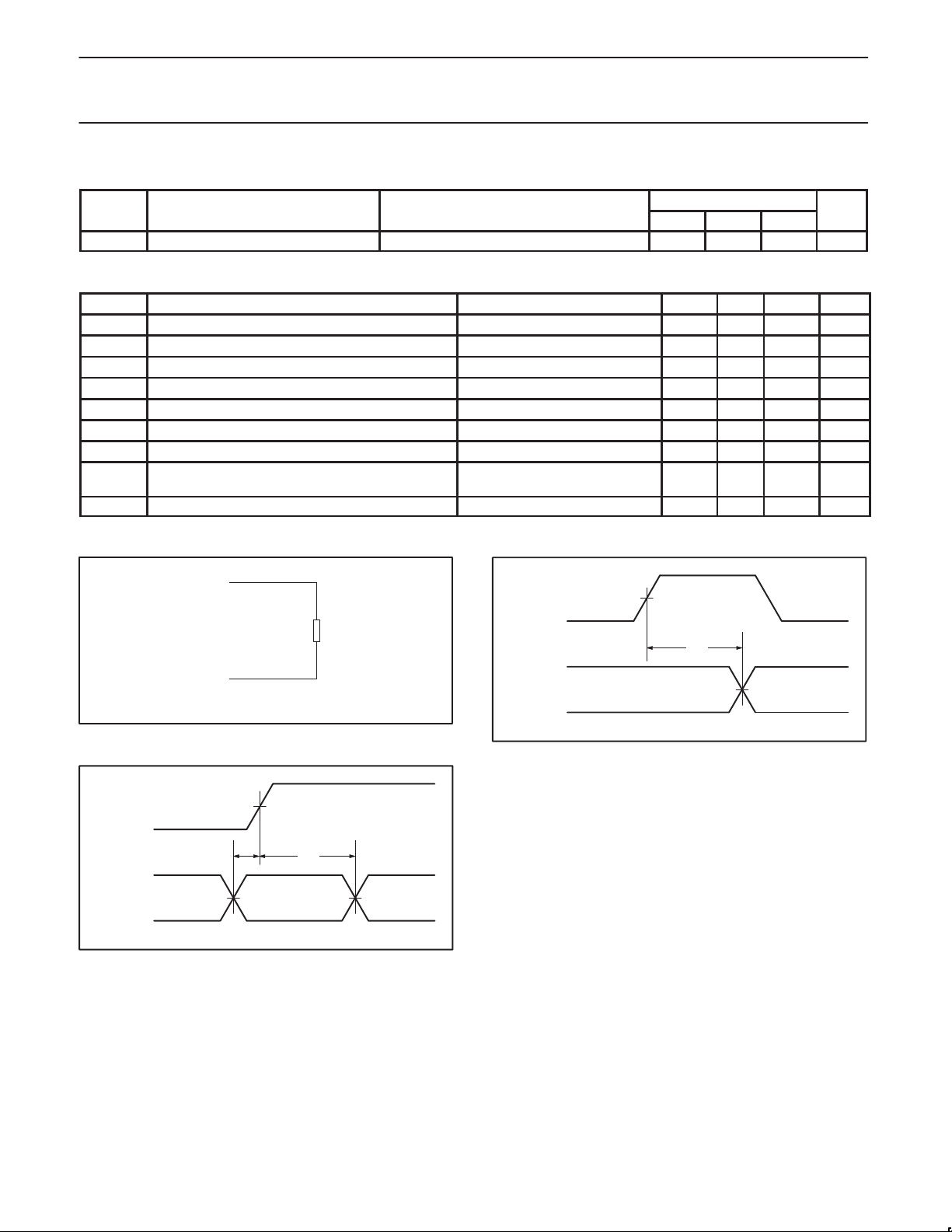
Setup time, CTL0, CTL1, D0–D7, LREQ to SYSCLK 50% to 50%; See Figure 2 5 — — ns
SU
t
Hold time, CTL0, CTL1, D0–D7, LREQ after SYSCLK 50% to 50%; See Figure 2 0 — — ns
H
t
Delay time SYSCLK to CTL0, CTL1, D0–D7 50% to 50%; See Figure 3 0.5 — 11 ns
D
Capacitance load value CTL0, CTL1, D0–D7,
L
SYSCLK
C
Input capacitance CTL0, CTL1, D0–D7, LREQ — 3.3 — pF
i
— 10 — pF
15.0 TIMING WAVEFORMS
TPAn+
TPBn+
56 Ω
TPAn–
TPBn–
SV01098
Figure 1. Test load diagram
SYSCLK
t
SU
Dn, CTLn, LREQ
Figure 2. Dn, CTLn, LREQ input setup and hold times
t
H
SV01099
SYSCLK
t
D
Dn, CTLn
SV01803
Figure 3. Dn, CTLn, output delay relative to SYSCLK
2001 Sep 06
14
 Loading...