

Philips pcx8598x DATASHEETS

INTEGRATED CIRCUITS
DATA SH EET
PCX8598X-2 Family
1024 × 8-bit CMOS EEPROMS
with I
Product specification
Supersedes data of April 1992
File under Integrated Circuits, IC12
Philips Semiconductors
2
C-bus interface
December 1994

Philips Semiconductors Product specification
1024 × 8-bit CMOS EEPROMS
with I
FEATURES
• Low power CMOS
– maximum active current 4.0 mA
– maximum standby current 10 µA (at 6.0 V),
• Non-volatile storage of 8-Kbits organized as four pages
of 256 × 8-bits each
• Single supply with full operation down to 2.5 V
• On-chip voltage multiplier
• Serial input/output I2C-bus
• Write operations
– byte write mode
– 8-byte page write mode
• Write-protection input
• Read operations
– sequential read
– random read
• Internal timer for writing (no external components)
• Power-on reset
• High reliability by using a redundant storage code
(single bit error correction)
• Endurance
– >500 k E/W-cycles at T
• 40 years non-volatile data retention time (typ.)
• Pin and address compatible to
– PCX8582X-2 Family and PCX8594X-2 Family.
2
C-bus interface
typical 4 µA
(minimizes total write time per byte)
=22°C
amb
PCX8598X-2 Family
DESCRIPTION
The PCX8598X-2 is an 8-Kbit (1024 × 8-bit) floating gate
electrically erasable programmable read only memory
(EEPROM). By using an internal redundant storage code
it is fault tolerant to single bit errors. This feature
dramatically increases reliability compared to conventional
EEPROM memories.
Power consumption is low due to the full CMOS
technology used. The programming voltage is generated
on-chip, using a voltage multiplier.
As data bytes are received and transmitted via the serial
I2C-bus, a package using eight pins is sufficient. Up to two
PCX8598X-2 devices may be connected to the I2C-bus.
Chip select is accomplished by one address input (A2).
Timing of the ERASE/WRITE cycle is carried out
internally, thus no external components are required. Pin 7
(PTC) must be connected to either VDD or left open-circuit.
There is an option of using an external clock for timing the
length of an ERASE/WRITE cycle.
A write-protection input at pin 1 (WP) allows disable of
write-commands from the master by a hardware signal.
When pin 1 is HIGH and one of the upper 512 EEPROM
cells is addressed, then the data bytes will not be
acknowledged by the PCX8598X-2 and the EEPROM
contents are not changed.
QUICK REFERENCE DATA
SYMBOL PARAMETER CONDITIONS MIN. MAX. UNIT
V
DD
I
DDR
I
DDW
I
DDSB
December 1994 2
supply voltage 2.5 6.0 V
supply current READ f
supply current ERASE/WRITE f
= 100 kHz
SCL
=3V − 60 µA
V
DD
=6V − 200 µA
V
DD
= 100 kHz
SCL
V
=3V − 1.0 mA
DD
=6V − 4.0 mA
V
DD
supply current STANDBY VDD=3V − 3.5 µA
=6V − 10 µA
V
DD
Philips Semiconductors Product specification
1024 × 8-bit CMOS EEPROMS
with I
ORDERING INFORMATION
PCF8598C-2P DIP8 plastic dual in-line package;
PCD8598D-2P −25 +70 3.0 6.0
PCF8598E-2P −40 +85 4.5 5.5
PCA8598F-2P −40 +125 4.5 5.5
PCF8598C-2T SO8 plastic small outline
PCD8598D-2T −25 +70 3.0 6.0
PCF8598E-2T −40 +85 4.5 5.5
PCA8598F-2T −40 +125 4.5 5.5
DEVICE SELECTION
Table 1 Device selection code
SELECTION DEVICE CODE CHIP ENABLE R/
Bit b7
Device 1 0 1 0 A2 MEM
2
C-bus interface
TYPE
NUMBER
P ACKAGE TEMPERA TURE (°C) SUPPLY (V)
NAME DESCRIPTION VERSION MIN. MAX. MIN. MAX.
SOT97-1 −40 +85 2.5 6.0
8 leads (300 mil)
SOT176-1 −40 +85 2.5 6.0
package;
8 leads; body width 7.5 mm
(1)
b6 b5 b4 b3 b2 b1 b0
PCX8598X-2 Family
MEM
SEL
SEL
R/
W
W
Note
1. The MSB b7 is sent first.
Table 2 Endurance and data retention guarantees
DEVICE ENDURANCE E/W CYCLES DATA RETENTION YEARS
PCF8598C-2; PCA8598F-2 500000
Note
1. At the time of publication of this data sheet the statistical history was not yet sufficient to guarantee 1000000000 E/W
cycle performance for these types.
(1)
40
December 1994 3
Philips Semiconductors Product specification
1024 × 8-bit CMOS EEPROMS
with I
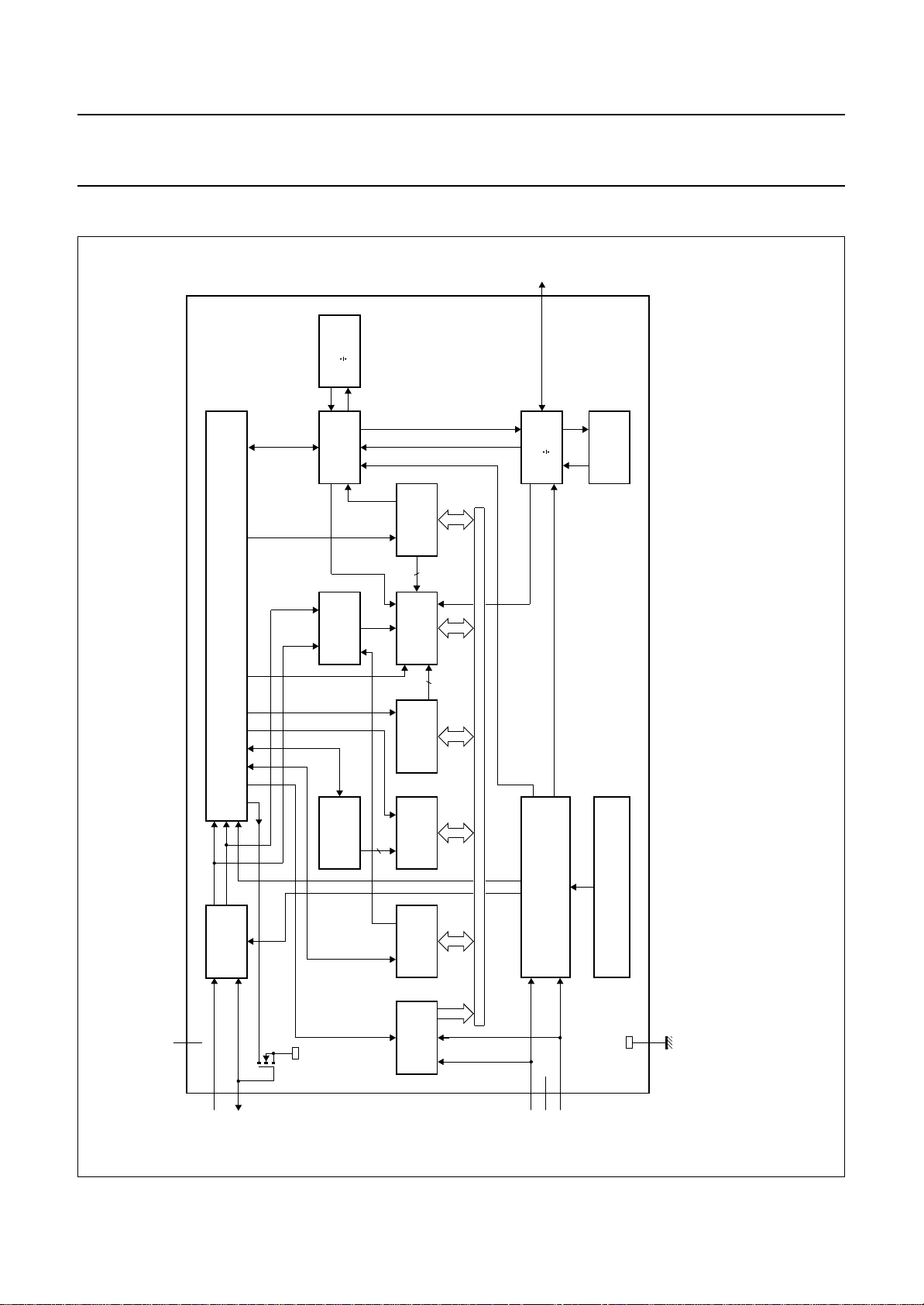
BLOCK DIAGRAM
2
C-bus interface
( 128)
DIVIDER
SEQUENCER
EE
CONTROL
4
PTC
7
( 16)
TIMER
PCX8598X-2 Family
MGA033 - 1
OSCILLATOR
HIGH
ADDRESS
2
I C - BUS CONTROL LOGIC
REGISTER
EEPROM
8
POINTER
ADDRESS
PCX8598X-2
handbook, full pagewidth
Fig.1 Block diagram.
BYTE
INPUT
FILTER
8
DD
V
6
n
5
3
COUNTER
BYTE
LATCH
(8 bytes)
SHIFT
REGISTER
SWITCH
ADDRESS
TEST MODE DECODER
321
POWER - ON RESET
SS
V
4
December 1994 4
SCL
SDA
A2
n.c.
WP

Philips Semiconductors Product specification
1024 × 8-bit CMOS EEPROMS
with I
2
C-bus interface
PINNING
SYMBOL PIN DESCRIPTION
WP 1 write-protection input
handbook, halfpage
WP
n.c. 2 not connected
A2 3 address input 2
V
SS
SDA 5 serial data input/output (I
SCL 6 serial clock input (I
4 negative supply voltage
2
C-bus)
2
C-bus)
PTC 7 programming time control output
V
DD
8 positive supply voltage
n.c.
A2
V
SS
Fig.2 Pin configuration.
LIMITING VALUES
In accordance with the Absolute Maximum Rating System (IEC134).
SYMBOL PARAMETER CONDITIONS MIN. MAX. UNIT
V
DD
V
I
I
I
I
O
T
stg
T
amb
supply voltage −0.3 +7.0 V
voltage on any input pin |ZI| > 500 Ω VSS− 0.8 VDD+ 0.8 V
current on any input pin − 1mA
output current − 10 mA
storage temperature −65 +150 °C
operating ambient temperature
PCF8598C-2; PCF8598E-2 −40 +85 °C
PCD8598D-2 −25 +70 °C
PCA8598F-2 −40 +125 °C
PCX8598X-2 Family
1
2
PCX8598X-2
3
4
MGA034 - 1
V
8
DD
PTC
7
SCL
6
5
SDA
December 1994 5
Philips Semiconductors Product specification
1024 × 8-bit CMOS EEPROMS
with I
2
C-bus interface
CHARACTERISTICS
PCF8598C-2: VDD= 2.5 to 6.0 V; VSS=0V; T
PCD8598D-2: VDD= 3.0 to 6.0 V; VSS=0V; T
PCF8598E-2: VDD= 4.5 to 5.5 V; VSS=0V; T
PCA8598F-2: VDD= 4.5 to 5.5 V; VSS=0V; T
= −40 to +85 °C; unless otherwise specified.
amb
= −25 to +70 °C; unless otherwise specified.
amb
= −40 to +85 °C; unless otherwise specified.
amb
= −40 to +125 °C; unless otherwise specified.
amb
SYMBOL PARAMETER CONDITIONS MIN. MAX. UNIT
Supplies
V
DD
supply voltage
PCF8598C-2 2.5 6.0 V
PCD8598D-2 3.0 6.0 V
PCF8598E-2; PCA8598F-2 4.5 5.5 V
I
DDR
I
DDW
I
DDSB
supply current READ f
PCF8598C-2; PCD8598D-2 V
PCF8598E-2; PCA8598F-2 V
supply current ERASE/WRITE f
PCF8598C-2; PCD8598D-2 V
PCF8598E-2; PCA8598F-2 V
supply current STANDBY f
PCF8598C-2; PCD8598D-2 V
PCF8598E-2; PCA8598F-2 V
= 100 kHz
SCL
= 3.0 V − 60 µA
DD
= 6.0 V − 200 µA
V
DD
= 5.5 V − 200 µA
DD
= 100 kHz
SCL
= 3.0 V − 1.0 mA
DD
= 6.0 V − 4.0 mA
V
DD
= 5.5 V − 4.0 mA
DD
= 100 kHz
SCL
= 3.0 V − 3.5 µA
DD
= 6.0 V − 10 µA
V
DD
= 5.5 V − 10 µA
DD
PTC input (pin 7)
V
IL
V
IH
LOW level input voltage −0.8 0.1V
HIGH level input voltage 0.9V
SCL input (pin 6)
V
IL
V
IH
I
LI
f
SCL
C
I
LOW level input voltage −0.8 0.3V
HIGH level input voltage 0.7V
input leakage current VI=VDDor V
SS
clock input frequency 0 100 kHz
input capacitance VI=V
SS
SDA input/output (pin 5)
V
IL
V
IH
V
OL
I
LO
C
I
LOW level input voltage −0.8 0.3V
HIGH level input voltage 0.7V
LOW level output voltage IOL= 3 mA; V
output leakage current VOH=V
input capacitance VI=V
SS
DD(min)
DD
Data retention time
t
S
data retention time T
=55°C10−years
amb
PCX8598X-2 Family
V
DD
VDD+ 0.8 V
DD
V
DD
VDD+ 0.8 V
DD
−±1µA
− 7pF
V
DD
VDD+ 0.8 V
DD
− 0.4 V
− 1 µA
− 7pF
December 1994 6
 Loading...