Philips PCKV857DGG Datasheet

INTEGRATED CIRCUITS
PCKV857
70–190 MHz differential 1:10 clock driver
Product data
Supersedes data of 2001 Mar 16
File under Intergrated Circuits ICL03
2001 Jun 12

Philips Semiconductors Product data
70–190 MHz differential 1:10 clock driver
FEA TURES
•ESD classification testing is done to JEDEC Standard JESD22.
Protection exceeds 2000 V to HBM per method A114.
•Latch-up testing is done to JEDEC Standard JESD78 which
exceeds 100 mA
•Optimized for clock distribution in DDR (Double Data Rate)
SDRAM applications as per JEDEC specifications
•1-to-10 differential clock distribution
•Very low skew (< 100 ps) and jitter (< 100 ps)
•Operation from 2.2 V to 2.7 V AV
•SSTL_2 interface clock inputs and outputs
•CMOS control signal input
•Test mode enables buffers while disabling PLL
•Low current power-down mode
•Tolerant of Spread Spectrum input clock
•Full DDR solution provided when used with SSTL16877 or
SSTV16857
•See PCKV856 for I
DESCRIPTION
The PCKV857 is a high-performance, low-skew, low-jitter zero delay
buffer designed for 2.5 V V
differential data input and output levels.
The PCKV857 is a zero delay buffer that distributes a differential
clock input pair (CLK, CLK
(Y[0:9], Y[0:9]
, FB
(FB
OUT
inputs (CLK, CLK
power input (AV
phase and frequency with CLK. When PWRDWN
are disabled to high impedance state (3-State), and the PLL is shut
down (low power mode). The device also enters the low power
mode when the input frequency falls below 20 MHz. An input
frequency detection circuit will detect the low frequency condition
and after applying a > 20 MHz input signal, the detection circuit
turns on the PLL again and enables the outputs.
When AV
purposes. The PCKV857 is also able to track spread spectrum
clocking for reduced EMI.
The PCKV857 is characterized for operation from 0 to +70 °C.
OUT
is grounded, the PLL is turned off and bypassed for test
DD
2
C capable clock driver
DD
) to ten differential pairs of clock outputs
) and one differential pair feedback clock outputs
) . The clock outputs are controlled by the clock
), the feedback clocks (FBIN, FBIN), and the analog
). When PWRDWN is high, the outputs switch in
DD
and 2.3 V to 2.7 V V
DD
and 2.5 V AVDD operation and
is low, all outputs
DD
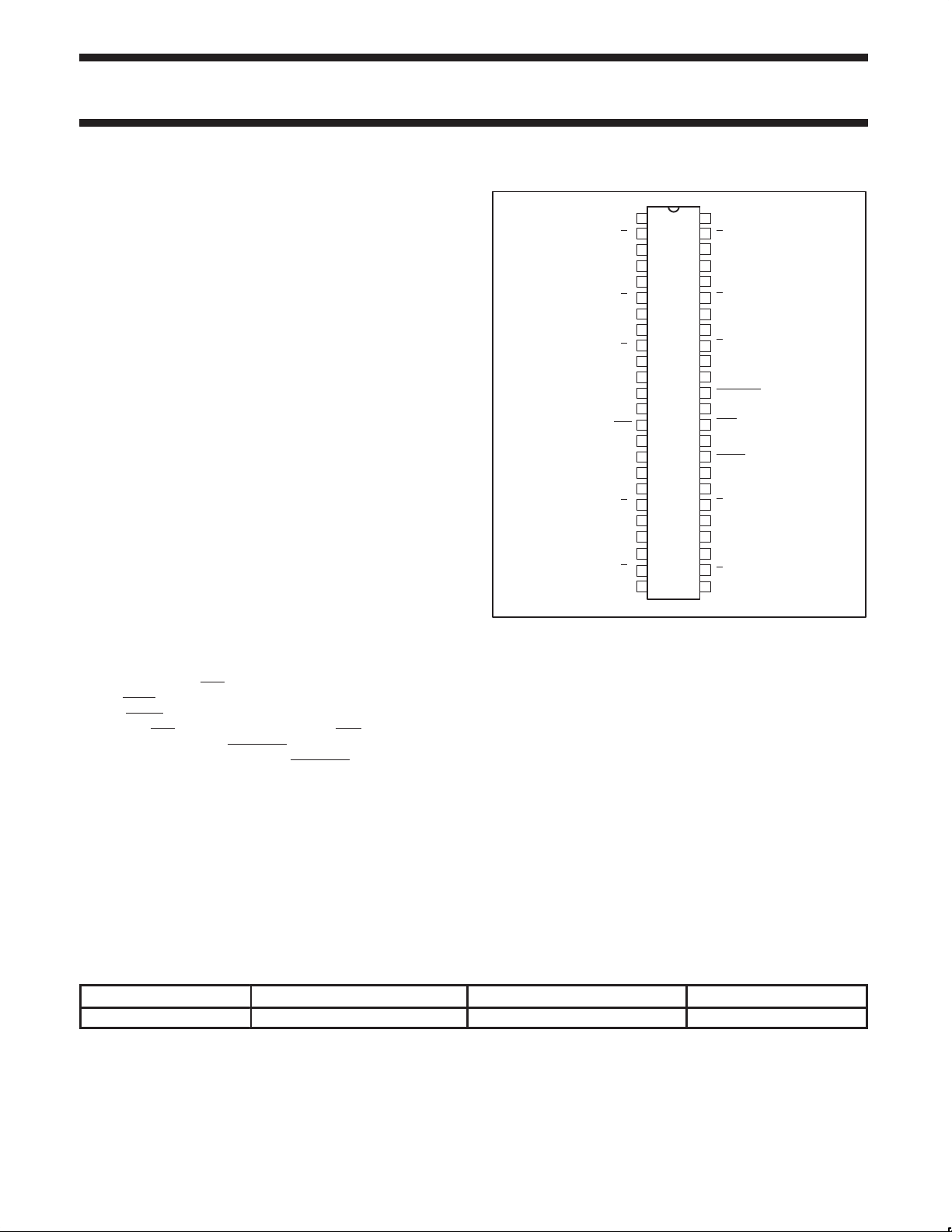
PIN CONFIGURATION
1
GND
Y
2
0
Y
3
0
4
V
DDQ
Y
5
1
Y
6
1
GND
7
8
GND
9
Y
2
Y
10
2
V
11
DDQ
V
12
DDQ
13
CLK
14
CLK
V
DDQ
15
AV
16
DD
17
AGND
GND
18
Y
19
3
Y
20
3
21
V
DDQ
Y
22
4
Y
4
23
24
GND
48
47
46
45
44
43
42
41
40
39
38
37
36
35
34
33
32
31
30
29
28
27
26
25
PCKV857
GND
Y
5
Y
5
V
DDQ
Y
6
Y
6
GND
GND
Y
7
Y
7
V
DDQ
PWRDWN
FB
IN
FB
IN
V
DDQ
FB
OUT
FB
OUT
GND
Y
8
Y
8
V
DDQ
Y
9
Y
9
GND
SW00691
ORDERING INFORMA TION
PACKAGES TEMPERATURE RANGE ORDER CODE DRAWING NUMBER
48-Pin Plastic TSSOP 0 to +70 °C PCKV857DGG SOT362-1
2001 Jun 12 853–2242 26485
2

Philips Semiconductors Product data
PLL ON/OFF
70–190 MHz differential 1:10 clock driver
PIN DESCRIPTION
PINS SYMBOL DESCRIPTION
1, 7, 8, 18, 24, 25, 31, 41, 42, 48 GND SSTL_2 ground pins
2, 3, 5, 6, 9, 10, 19, 20, 22, 23, 26, 27, 29,
30, 32, 33, 39, 40, 43, 44, 46, 47
4, 11, 12, 15, 21, 28, 34, 38, 46 V
13, 14, 35, 36 CLKIN, CLKIN, FBIN, FB
16 AV
17 AGND Analog ground
37 PWRDWN Power-down control input
FUNCTION TABLE
INPUTS OUTPUTS
PWRDWN CLK CLK Y
L L H Z Z Z
L H L Z Z Z
H L H L H L H ON
H H L H L H L ON
2
X
NOTES:
H = HIGH voltage level
L = LOW voltage level
Z = high impedance OFF-state
X = don’t care
1. Subject to change. May cause conflict with FB
2. Additional feature that senses when the clock input is less than 20 MHz and places the part in sleep mode.
< 20 MHz < 20 MHz Z Z Z
pins.
IN
Yn, Yn, FB
n
OUT
DDQ
DD
, FB
OUT
Y
SSTL_2 differential outputs
SSTL_2 power pins
IN
SSTL_2 differential inputs
Analog power
n
FB
OUT
1
1
1
FB
OUT
Z
Z
Z
1
1
1
PCKV857
OFF
OFF
OFF
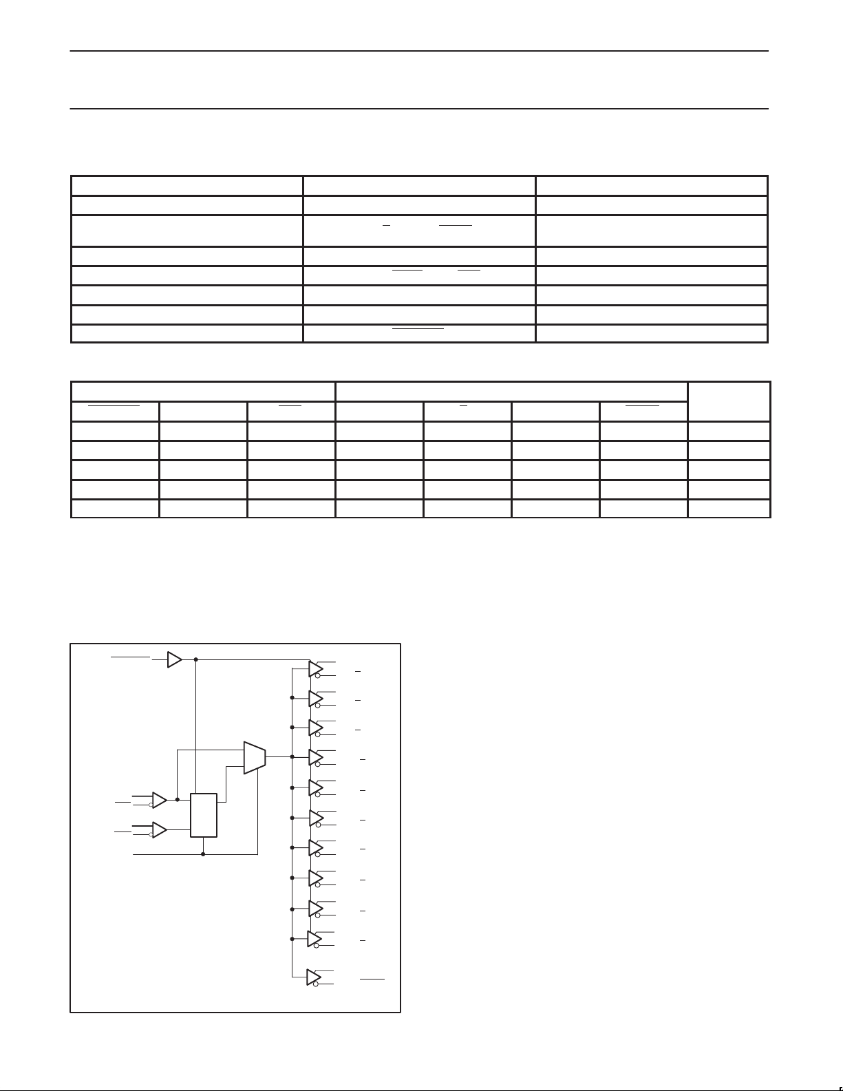
BLOCK DIAGRAM
37 – PWRDWN
13 – CLK
14 – CLK
36 – FB
IN
35 – FB
IN
16 – AV
DD
PLL
3 – Y
2 – Y
5 – Y
6 – Y
10 – Y
9 – Y
20 – Y
19 – Y
22 – Y
23 – Y
46 – Y
47 – Y
44 – Y
43 – Y
39 – Y
40 – Y
29 – Y
30 – Y
27 – Y
28 – Y
32 – FB
33 – FB
SW00692
0
0
1
1
2
2
3
3
4
4
5
5
6
6
7
7
8
8
9
9
OUT
OUT
2001 Jun 12
3

Philips Semiconductors Product data
SYMBOL
PARAMETER
CONDITION
UNIT
SYMBOL
PARAMETER
CONDITION
UNIT
IL
g
IH
gg
V
70–190 MHz differential 1:10 clock driver
ABSOLUTE MAXIMUM RATINGS
1
PCKV857
LIMITS
MIN MAX
V
AV
DDQ
V
V
I
IK
I
OK
I
O
T
stg
DD
O
Supply voltage range 0.5 3.6 V
Supply voltage range 0.5 3.6 V
Input voltage range see Notes 2 and 3 –0.5 V
I
Output voltage range see Notes 2 and 3 –0.5 V
Input clamp current VI < 0 or VI >V
Output clamp current VO < 0 or VO >V
Continuous output current VO = 0 to V
Continuous current to GND or V
DDQ
DDQ
DDQ
DDQ
— ±50 mA
— ±50 mA
— ±50 mA
— ±100 mA
Storage temperature range –65 +150 °C
+ 0.5 V
DDQ
+ 0.5 V
DDQ
NOTES:
1. Stresses beyond those listed under “absolute maximum ratings” may cause permanent damage to the device. These are stress ratings
only, and functional operation of the device at these or any other conditions beyond those indicated under “recommended operating
conditions” is not implied. Exposure to absolute-maximum-rated conditions for extended periods may affect device reliability .
2. The input and output negative voltage ratings may be exceeded if the input and output clamp-current ratings are observed.
3. This value is limited to 3.6 V maximum.
RECOMMENDED OPERATING CONDITIONS
1
LIMITS
MIN TYP MAX
V
AV
DDQ
V
Supply voltage range 2.3 — 2.7 V
Supply voltage range 2.2 — 2.7 V
DD
Low level input voltage
IL
CLK, CLK,
FBIN, FB
IN
— — V
DDQ
/2 − 0.18
V
PWRDWN −0.3 — 0.7
CLK, CLK,
V
High level input voltage
IH
FBIN, FB
IN
PWRDWN 1.7 — V
DC input signal voltage Note 2 −0.3 — V
DC differential input signal voltage CLK, FB
ID
AC differential input signal voltage CLK, FB
V
V
I
OH
I
OL
Output differential cross-voltage Note 4 V
OX
Input differential cross-voltage Note 4 V
IX
High-level output current — — −12 mA
Low-level output current — — 12 mA
IN
IN
Note 3 0.36 — V
Note 3 0.7 — V
V
/2 + 0.18 — —
DDQ
/2 − 0.2 V
DDQ
/2 − 0.2 — V
DDQ
DDQ
/2 V
+ 0.3
DDQ
DDQ
+ 0.6 V
DDQ
+ 0.6 V
DDQ
/2 + 0.2 V
DDQ
/2 + 0.2 V
DDQ
V
V
SR Input slew rate 1 — 4 V/ns
T
amb
Operating free-air temperature 0 — 70 °C
NOTES:
1. Unused inputs must be held high or low to prevent them from floating.
2. DC input signal voltage specifies the allowable DC execution of differential input.
3. Differential input signal voltage specifies the differential voltage |VTR – VCP| required for switching, where VTR is the true input level and
VCP is the complementary input level.
4. Differential cross-point voltage is expected to track variations of V
and is the voltage at which the differential signals must be crossing.
CC
2001 Jun 12
4
 Loading...