

Philips PCK2000MDB Datasheet

INTEGRATED CIRCUITS
PCK2000M
CK97 (66/100MHz) Mobile System Clock
Generator
Product specification 1998 Sep 29

Philips Semiconductors Product specification
PCK2000MCK97 (66/100MHz) Mobile System Clock Generator
FEA TURES
•Reduced pincount version of PCK2000 for mobile applications
•Mixed 2.5V and 3.3V operation
•Two CPU clocks at 2.5V
•Six synchronous PCI clocks at 3.3V, one free–running
•One 3.3V reference clock @ 14.318 MHz
•Reference 14.31818 MHz Xtal oscillator input
•100 MHz or 66 MHz operation
•Power management control input pins
•175 ps CPU clock jitter
•175 ps skew on outputs
•Available in 28–pin SSOP package
•1.5 – 4ns CPU–PCI delay
•Power down if PWRDWN is held LOW
•See PCK2000 for 48-pin version
DESCRIPTION
The PCK2000M is a clock synthesizer/driver chip for a Pentium Pro
or other similar processors, typically used in mobile applications.
The PCK2000M has two CPU clock outputs at 2.5V. There are six
PCI clock outputs running at 33 MHz. One of the PCI clock outputs
is free–running. The 3.3V reference clock outputs at 14.318 MHz.
All clock outputs meet Intel’s drive strength, rise/fall time, jitter,
accuracy, and skew requirements.
The part possesses dedicated powerdown, CPUSTOP, and
PCISTOP input pins for power management control. These inputs
are synchronized on–chip and ensure glitch–free output transitions.
When the CPUSTOP input is asserted, the CPU clock outputs are
driven LOW. When the PCIST OP inputs is asserted, the PCI clock
outputs are driven LOW.
Finally, when the PWRDWN input pin is asserted, the internal
reference oscillator and PLLs are shut down, and all outputs are
driven LOW, except the free running PCICLK_F clock output.
The PCK2000M is available in a 28–pin SSOP package.
PIN CONFIGURATION
XTAL IN
OUT V
XTAL
V
SSPCI0
PCICLK_F
PCICLK1
V
DDPCI0
PCICLK2
PCICLK3
V
DDPCI1
V
SSPCI1
DDCORE0
SSCORE0
10
11
12 17
13 16V
14 15V
PCICLK4
PCICLK5 CPUSTOP
V
1
227
3
4
5
6
7
8
9
TOP VIEW
28
SSREF
DDREF
REF
26
25
V
DDCPU
24
CPUCLK0
23
CPUCLK1
22
V
SSCPU
21
V
DDCORE1
20
V
19
18
SSCORE1
PCISTOP
PWRDWN
SEL
SEL100/66
SA00448
PCK2000M
ORDERING INFORMATION
PACKAGES TEMPERATURE RANGE OUTSIDE NORTH AMERICA NORTH AMERICA DRAWING NUMBER
28-Pin Plastic SSOP 0°C to +70°C PCK2000M DB PCK2000M DB SOT341-1
Intel and Pentium are registered trademarks of Intel Corporation.
1998 Sep 29 853-2128 20101
2
Philips Semiconductors Product specification
CK97 (66/100MHz) Mobile System Clock Generator
PCK2000M
PIN DESCRIPTION
PIN NUMBER SYMBOL FUNCTION
26 REF 14.318 MHz clock output
28 V
27 V
SSREF
DDREF
1 XTAL_IN 14.318 MHz crystal input
2 XTAL_OUT 14.318 MHz crystal output
3, 12 V
[0–1] GROUND for PCI outputs
SSPCI
4 PCICLK_F Free-running PCI output
6, 9 V
[0–1] POWER for PCI outputs
DDPCI
5, 7, 8, 10, 11 PCICLK [1–5] PCI clock outputs.
13, 21 V
14, 20 V
[0–1] Isolated POWER for core
DDCORE
[0–1] Isolated GROUND for core
SSCORE
16 SEL Logic select pins
15 SEL100/66
17 PWRDWN Control pin to put device in powerdown state, active low
18 CPUSTOP Control pin to disable CPU clocks, active low
19 PCISTOP Control pin to disable PCI clocks, active low
25 V
22 V
DDCPU
SSCPU
23, 24 CPUCLK [0–1] CPU and Host clock outputs 2.5V
NOTE:
1. V
and VSS names in the above tables reflects a likely internal POWER and GROUND partition to reduce the effects of internal noise on
DD
the performance of the device. In reality, the platform will be configured with the V
tied to a common 3.3V supply and all V
pins being common.
SS
GROUND for REF output
POWER for REF output
Select pin for enabling 66 MHz or 100MHz or 66 MHz. L = 66 Mhz
H = 100MHz
Power for CPU outputs
GROUND for CPU outputs
pins tied to a 2.5V supply, all remaining V
DDCPU
DD
pins
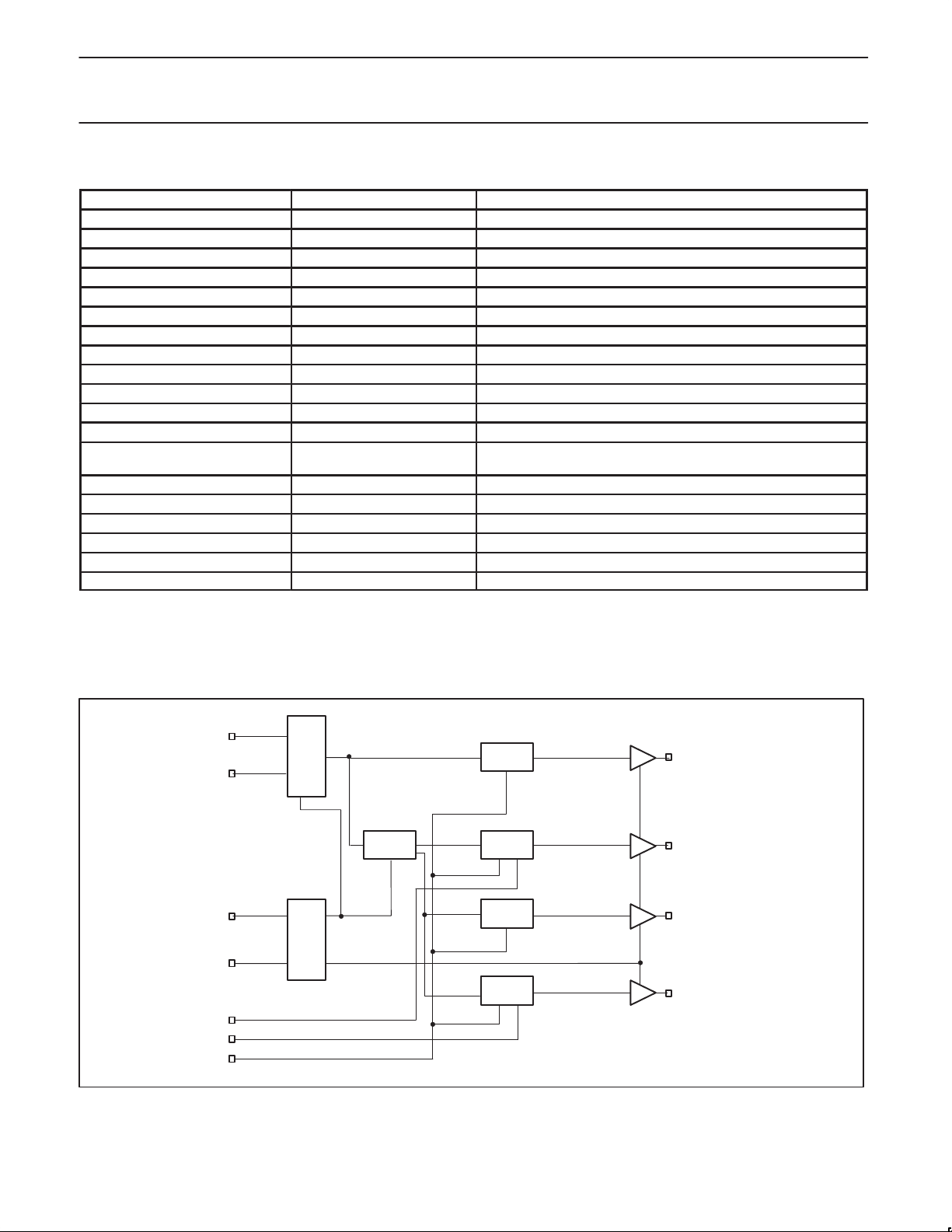
BLOCK DIAGRAM
XTAL_IN
XTAL_OUT
SEL100/66
CPUSTOP
PCISTOP
PWRDWN
SEL0
X
X
X
X
X
X
X
14.318
MHZ
OSC
LOGIC
PLL1
PWRDWN
LOGIC
STOP
LOGIC
PWRDWN
LOGIC
STOP
LOGIC
REFCLK (14.318 MHz)
X
CPUCLK [0–1]
X
PCICLK_F (33MHz)
X
PCICLK [1–5] (33MHz)
X
SW00275
1998 Sep 29
3
Philips Semiconductors Product specification
CK97 (66/100MHz) Mobile System Clock Generator
SELECT FUNCTIONS
SEL100/66 SEL0 FUNCTION NOTES
0 0 TRI-State 1
0 1 Active 66MHz
1 0 Test mode 1
1 1 Active 100MHz
NOTES:
1. Internal decode logic for all two select inputs implemented.
FUNCTION
DESCRIPTION
Tri-State Hi-Z Hi-Z Hi-Z
Test mode TCLK/2 TCLK/6 TCLK
FUNCTION TABLE
SEL 100/66 CPU/PCI RATIO
0 2 66.66 33.33 14.318
1 3 100 33.33 14.318
CPU PCI, PCI_F REF
CPUCLK (0–1)
(MHz)
OUTPUTS
CPICLK (1–5)
PCICLK_F
(MHz)
PCK2000M
REF
(MHz)
CLOCK ENABLE CONFIGURATION
CPUSTOP PCISTOP PWRDWN CPUCLK PCICLK PCICLK_F
X X 0 LOW LOW LOW Stopped OFF OFF
0 0 1 LOW LOW 33MHz Running Running Running
0 1 1 LOW 33MHz 33MHz Running Running Running
1 0 1 100/66MHz LOW 33MHz Running Running Running
1 1 1 100/66MHz 33MHz 33MHz Running Running Running
OTHER
CLOCKS
PLL OSCILLATOR
POWER MANAGEMENT REQUIREMENTS
LATENCY
SIGNAL SIGNAL STATE
CPUSTOP 0 (DISABLED) 1
1 (ENABLED) 1
PCISTOP 0 (DISABLED) 1
1 (ENABLED) 1
PWRDWN 1 (NORMAL OPERATION) 3ms
0 (POWER DOWN) 2 MAX
NOTES:
1. Clock ON/OFF latency is defined as the number of rising edges of free running PCICLKs between the clock disable goes HIGH/LOW to the
first valid clock that comes out of the device.
2. Power up latency is when PWRDWN goes inactive (HIGH) to when the first valid clocks are driven from the device.
NO. OF RISING EDGES OF FREE RUNNING
PCICLK
1998 Sep 29
4
 Loading...