

Philips PCK2000DL Datasheet

INTEGRATED CIRCUITS
PCK2000
CK97 (66/100MHz) System Clock
Generator
Product specification 1998 Sep 29
Philips Semiconductors Product specification
PCK2000CK97 (66/100MHz) System Clock Generator
FEA TURES
•Mixed 2.5V and 3.3V operation
•Four CPU clocks at 2.5V
•Eight synchronous PCI clocks at 3.3V, one free-running
•Two 2.5V IOAPIC clocks @ 14.318 MHz
•Two 3.3V 48MHz USB clock outputs
•Three 3.3V reference clocks @ 14.318 MHz
•Reference 14.31818 MHz Xtal oscillator input
•100 MHz or 66 MHz operation
•Part provides frequencies for Pentium Pro and
Pentium II motherboards
•Power management control input pins
•175 ps CPU clock jitter
•175 ps skew on outputs
•1.5 – 4 ns CPU–PCI delay
•Power down if PWRDWN is held LOW
•Available in 48-pin SSOP package
•See PCK2000M for 28-pin mobile version
DESCRIPTION
The PCK2000 is a clock synthesizer/driver chip for a Pentium Pro or
other similar processors.
The PCK2000 has four CPU clock outputs at 2.5V . There are eight
PCI clock outputs running at 33MHz. One of the PCI clock outputs is
free-running. Additionally, the part has two 3.3V USB clock outputs
at 48MHz, two 2.5V IOAPIC clock outputs at 14.318MHz, and three
3.3V reference clock outputs at 14.318MHz. All clock outputs meet
Intel’s drive strength, rise/fall time, jitter , accuracy, and skew
requirements.
The part possesses dedicated powerdown, CPUSTOP, and
PCISTOP input pins for power management control. These inputs
are synchronized on-chip and ensure glitch-free output transitions.
When the CPUSTOP input is asserted, the CPU clock outputs are
driven LOW. When the PCIST OP input is asserted, the PCI clock
outputs are driven LOW, except for free running PCICLK_F clock
output..
Finally, when the PWRDWN input pin is asserted, the internal
reference oscillator and PLLs are shut down, and all outputs are
driven LOW.
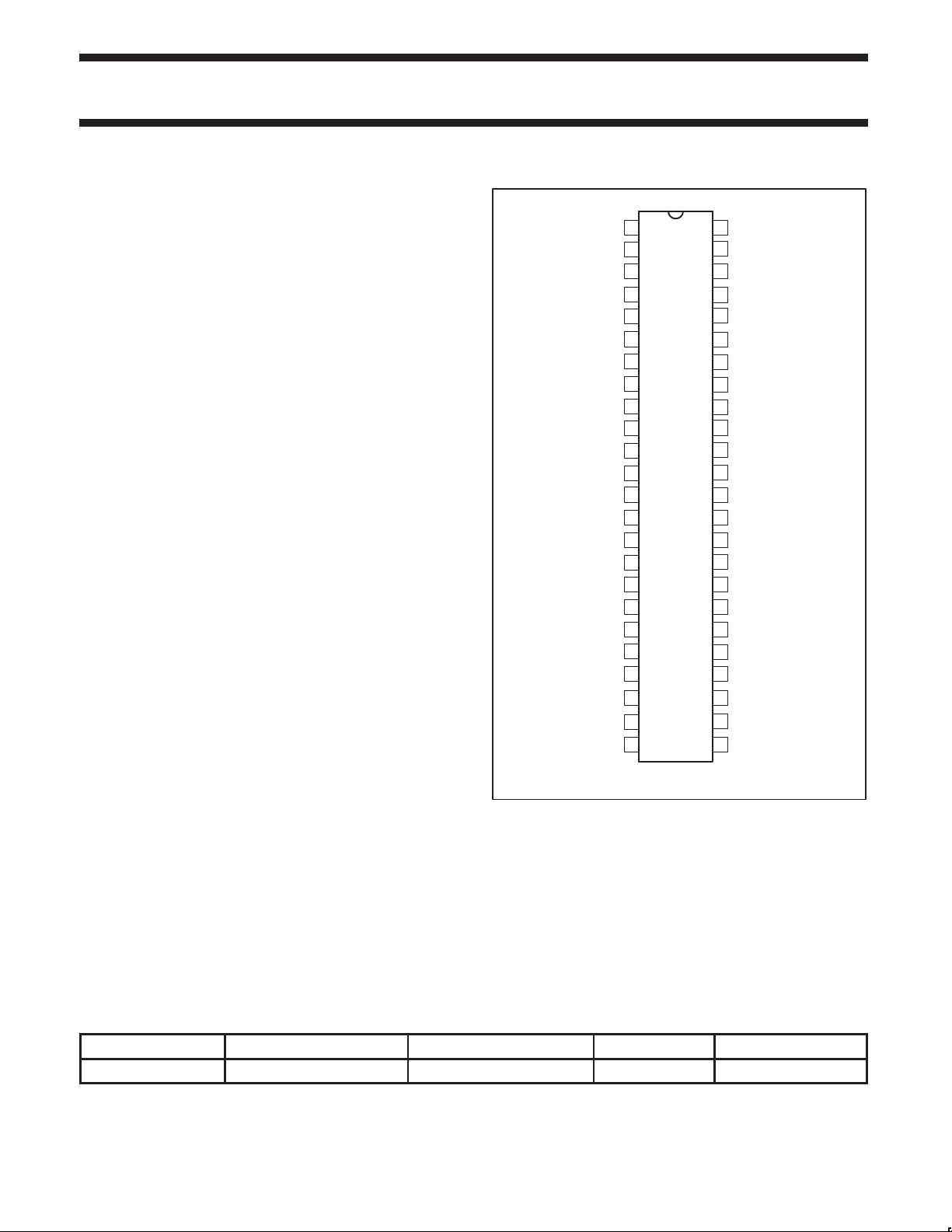
The PCK2000 is available in a 48–pin SSOP package.
PIN CONFIGURATION
1
REF0
REF1
2
V
3
SSREF
V
SSPCI0
V
DDPCI0
V
SSPCI1
V
DDPCI1
V
SSPCI2
SSCORE0
48MHz0
48MHz1
48MHz
4
5
6
7
8
9
10
11
12
13
14
15
16
17
18
19
20
21
22
23
24
XTAL_IN
XTAL_OUT
PCICLK_F
PCICLK1
PCICLK2
PCICLK3
PCICLK4
PCICLK5
PCICLK6
PCICLK7
V
DDCORE0
V
VDD48MHz
V
SS
48
V
47
REF2
46
V
45
IOAPIC0
44
IOAPIC1
43
V
42
RESERVED
41
V
40
CPUCLK0
39
CPUCLK1
V
38
37
V
36
CPUCLK2
PCK2000
35
CPUCLK3
V
34
33
V
32
V
31
PCISTOP
30
CPUSTOP
29
PWRDWN
RESERVED
28
27
SEL0
SEL1
26
SEL100/66
25
SW00237
DDREF
DDAPIC
SSAPIC
DDCPU0
SSCPU0
DDCPU1
SSCPU1
DDCORE1
SSCORE1
ORDERING INFORMA TION
PACKAGES TEMPERATURE RANGE OUTSIDE NORTH AMERICA NORTH AMERICA DRAWING NUMBER
48-Pin Plastic SSOP 0°C to +70°C PCK2000 DL PCK2000 DL SOT370-1
Intel and Pentium are registered trademarks of Intel Corporation.
1998 Sep 29 853-2129 20102
2

Philips Semiconductors Product specification
CK97 (66/100MHz) System Clock Generator
PIN DESCRIPTION
PIN NUMBER SYMBOL FUNCTION
1, 2, 47 REF [0–2] 14.318 MHz clock outputs
3 V
48 V
SSREF
DDREF
4 XTAL_IN 14.318 MHz crystal input
5 XTAL_OUT 14.318 MHz crystal output
6, 12, 18 V
[0–2] GROUND for PCI outputs
SSPCI
7 PCICLK_F Free-running PCI output
9, 15 V
[0–1] POWER for PCI outputs
DDPCI
8, 10, 11, 13, 14, 16, 17 PCICLK [1–7] PCI clock outputs.
19, 33 V
20, 32 V
[0–1] Isolated POWER for core
DDCORE
[0–1] Isolated GROUND for core
SSCORE
21 VDD 48MHz POWER for 48MHz outputs
24 VSS 48MHz GROUND for 48MHz outputs
22, 23 48MHz [0–1] 48MHz outputs
26, 27 SEL0,1 Logic select pins.
25 SEL100/66
29 PWRDWN Control pin to put device in powerdown state, active low
30 CPUSTOP Control pin to disable CPU clocks, active low
31 PCISTOP Control pin to disable PCI clocks, active low
37, 41 V
34, 38 V
[0–1] POWER for CPU outputs
DDCPU
[0–1] GROUND for CPU outputs
SSCPU
35, 36, 39, 40 CPUCLK [0–3] CPU clock outputs @2.5V
43 V
46 V
SSAPIC
DDAPIC
44, 45 IOAPIC [0–1] IOAPIC output @ 2.5V
28, 42 RESERVED Reserved for future use
NOTES:
and VSS names in the above tables reflects a likely internal POWER and GROUND partition to reduce the effects of internal noise on
1. V
DD
the performance of the device. In reality, the platform will be configured with the V
remaining V
pins tied to a common 3.3V supply and all VSS pins being common.
DD
GROUND for REF outputs
POWER for REF outputs
Select pin for enabling 66 MHz or 100MHz. L = 66 MHz
H = 100MHz
GROUND for IOAPIC outputs
POWER for IOAPIC outputs
DDAPIC
and V
pins tied to a 2.5V supply, all
DDCPU
PCK2000
1998 Sep 29
3
Philips Semiconductors Product specification
CK97 (66/100MHz) System Clock Generator
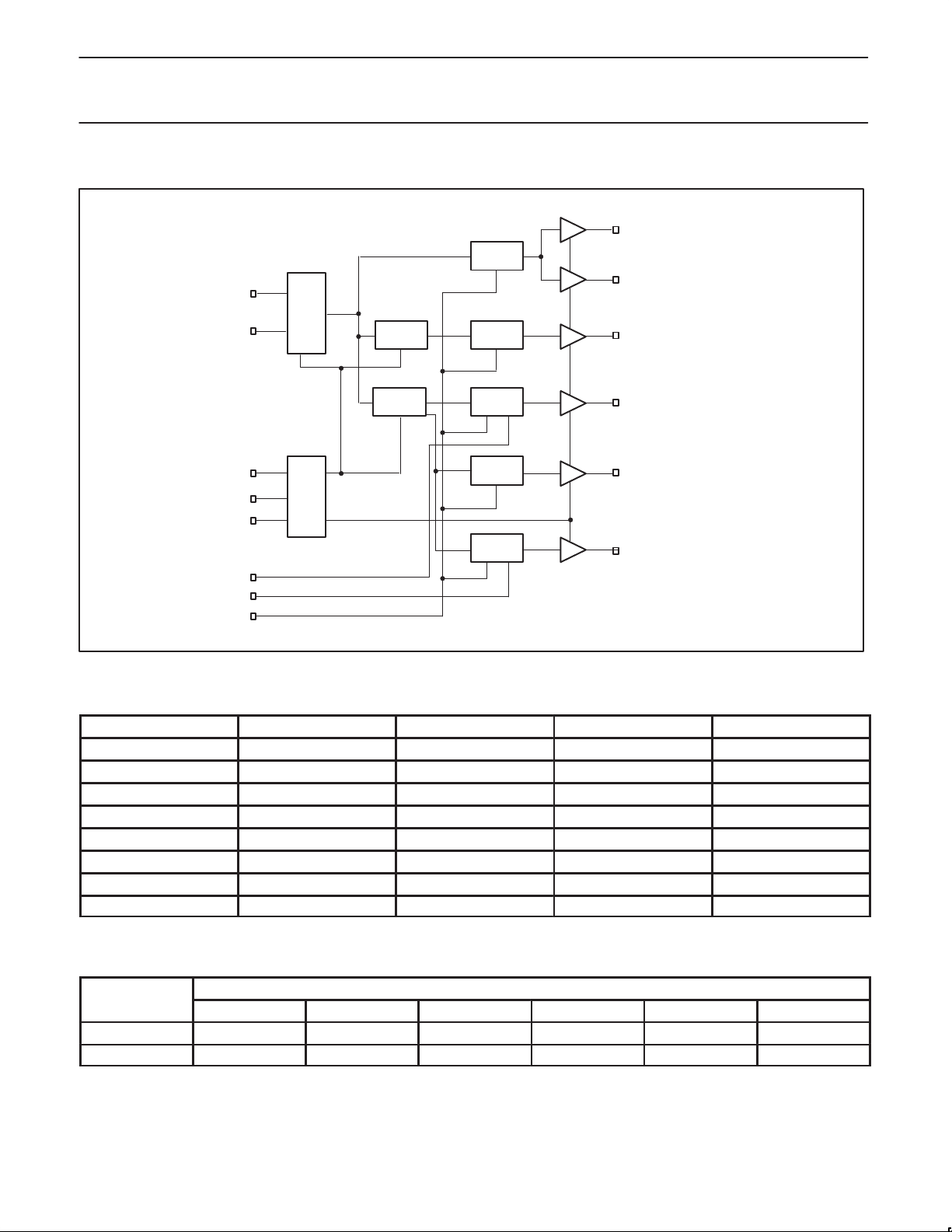
BLOCK DIAGRAM
PWRDWN
XTAL_IN
X
14.318
MHZ
XTAL_OUT
SEL0
SEL1
SEL100/66
CPUSTOP
PCISTOP
PWRDWN
OSC
X
X
LOGIC
X
X
X
X
X
PLL2
PLL1
PWRDWN
PWRDWN
LOGIC
LOGIC
STOP
LOGIC
LOGIC
STOP
LOGIC
REFCLK [0–2](14.318 MHz)
X
IOAPIC [0–1](14.318 MHz)
X
X
48MHz [0–1](48MHz)
CPUCLK [0–3] (100MHz/66MHz)
X
PCICLK_F (33MHz)
X
PCICLK [1–7](33MHz)
X
SW00236
PCK2000
SELECT FUNCTIONS
SEL100/66 SEL1 SEL0 FUNCTION NOTES
0 0 0 TRI-State 1
0 0 1 Reserved
0 1 0 Reserved
0 1 1 Active 66MHz
1 0 0 Test mode 1
1 0 1 Reserved
1 1 0 Reserved
1 1 1 Active 100MHz
NOTE:
1. Internal decode logic for all three select inputs implemented.
FUNCTION
DESCRIPTION
CPU PCI, PCI_F 48MHz REF IOAPIC NOTES
3-STATE HI-Z HI-Z HI-Z HI-Z HI-Z
TEST MODE TCLK/2 TCLK/6 TCLK/2 TCLK TCLK
NOTE:
1. TCLK is a test clock driven in on the XTAL_IN input in Test Mode.
OUTPUTS
1998 Sep 29
4
Philips Semiconductors Product specification
CK97 (66/100MHz) System Clock Generator
FUNCTION TABLE
SEL 100/66 CPU/PCI RATIO
0 2 66.66 33.33 14.318 48
1 3 100 33.33 14.318 48
CPUCLK (0–3)
(MHz)
CPICLK (1–7)
PCICLK_F
(MHz)
CLOCK ENABLE CONFIGURATION
CPUSTOP PCISTOP PWRDWN CPUCLK PCICLK PCICLK_F
X X 0 LOW LOW LOW Stopped OFF OFF
0 0 1 LOW LOW 33MHz Running Running Running
0 1 1 LOW 33MHz 33MHz Running Running Running
1 0 1 100/66MHz LOW 33MHz Running Running Running
1 1 1 100/66MHz 33MHz 33MHz Running Running Running
REF (0–2)
IOAPIC (0–1)
(MHz)
OTHER
CLOCKS
PLLs OSCILLATOR
PCK2000
48MHz (0–1)
POWER MANAGEMENT REQUIREMENTS
LATENCY
SIGNAL SIGNAL STATE
CPUSTOP 0 (DISABLED) 1
1 (ENABLED) 1
PCISTOP 0 (DISABLED) 1
1 (ENABLED) 1
PWRDWN 1 (NORMAL OPERATION) 3ms
0 (POWER DOWN) 2 MAX
NOTES:
1. Clock ON/OFF latency is defined as the number of rising edges of free running PCICLKs between the clock disable goes HIGH/LOW to the
first valid clock that comes out of the device.
2. Power up latency is when PWRDWN goes inactive (HIGH) to when the first valid clocks are driven from the device.
NO. OF RISING EDGES OF FREE RUNNING
PCICLK
1998 Sep 29
5
 Loading...