


INTEGRATED CIRCUITS
PCK111
Low voltage 1:10 differential
PECL clock driver
Product data
File under Integrated Circuits — ICL03
2001 Sep 07
Philips Semiconductors Product data
Type number
p
Low voltage 1:10 differential
PECL clock driver
FEA TURES
•100 ps part-to-part skew typical
•35 ps output-to-output skew typical
•Differential design
•V
output
BB
•Low voltage V
•75 kΩ input pull-down resistors
•ECL/PECL outputs
•Form, fit, and function compatible with MC100EP111
DESCRIPTION
The PCK111 is a low skew 1-to-10 differential driver, designed with
clock distribution in mind. It accepts two clock sources into an input
multiplexer. The PECL input signals can be either differential or
single-ended if the VBB output is used. The selected signal is fanned
out to 10 identical differential outputs.
The PCK111 is specifically designed, modeled and produced with
low skew as the key goal. Optimal design and layout serve to
minimize gate-to-gate skew within a device, and empirical modeling
is used to determine process control limits that ensure consistent
t
distributions from lot to lot. The net result is a dependable,
PD
guaranteed low skew device.
To ensure that the tight skew specification is met, it is necessary that
both sides of the differential output are terminated into 50 Ω, even if
only one side is being used. In most applications, all ten differential
pairs will be used, and therefore terminated. In the case where fewer
than ten pairs are used, it is necessary to terminate at least the
output pairs on the same package side as the pair(s) being used on
that side, in order to maintain minimum skew. Failure to do this will
result in small degradations of propagation delay (on the order of
10–20 ps) of the output(s) being used, which, while not being
catastrophic to most designs, will mean a loss of skew margin.
The PCK111 can be used for high performance clock distribution in
+3.3 V or +2.5 V system s. Designers can take advantage of the
PCK111’s performance to distribute low skew clocks across the
backplane or the board. In a PECL environment, series or Thevenin
line terminations are typically used as they require no additional
power supplies.
The PCK111 may be driven single-endedly utilizing the V
output with the CLK0
pin should be connected to the CLK0 input and bypassed to
the V
BB
ground via a 0.01 µF capacitor. The V
0.2 mA, therefore, it should be used as a switching reference for the
PCK111 only. Part-to-part skew specifications are not guaranteed
when driving the PCK111 single-endedly.
range of +2.375 V to +3.8 V for PECL
CC
input. If a single-ended signal is to be used,
output can only source/sink
BB
BB
bias
PCK1 11
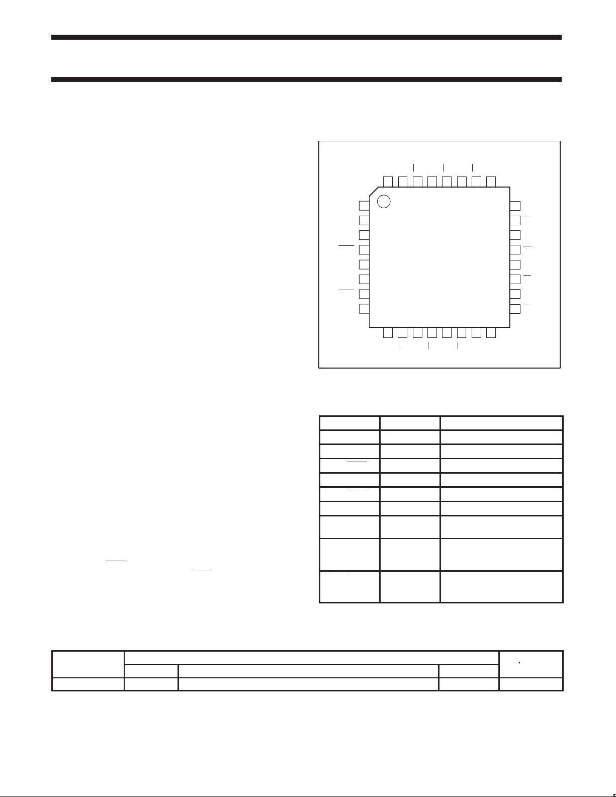
PINNING
Pin configuration
CCO
V
Q0
Q0
Q1
Q1
Q2
32
31
30
29
28
27
V
1
CC
CLK0
CLK0
V
CLK1
CLK1
V
2
3
4
5
BB
6
7
8
EE
9
CCO
V
10
Q9
PCK111
11
12
Q9
Q8
13
Q8
14
Q7
CLK_SEL
Figure 1. Pin configuration
Pin description
SYMBOL PIN DESCRIPTION
V
CC
CLK_SEL 2 Active clock select input
CLK0, CLK0 3, 4 Differential ECL/PECL input pair
V
BB
CLK1, CLK1 6, 7 Differential HSTL input pair
V
EE
V
CCO
Q0–Q9 31, 29, 27, 24,
Q0–Q9 30, 28, 26, 23,
1 Supply voltage
5 VBB output
8 Ground
9, 16, 25, 32 Output drive power supply
voltage
Differential PECL outputs
22, 20, 18, 15,
13, 11
Differential PECL outputs
21, 19, 17, 14,
12, 10
Q2
26
15
Q7
V
25
16
V
CCO
CCO
24
Q3
23
Q3
22
Q4
Q4
21
Q5
20
Q5
19
Q6
18
Q6
17
SW00907
ORDERING INFORMATION
Package
Name Description Version
PCK111BD LQFP32 plastic low profile quad flat package; 32 leads; body 7 × 7 × 1.4 mm SOT358-1 –40 to +70 °C
2001 Sep 07 853-2281 27052
2
Temperature
range
Philips Semiconductors Product data
Low voltage 1:10 differential
PECL clock driver
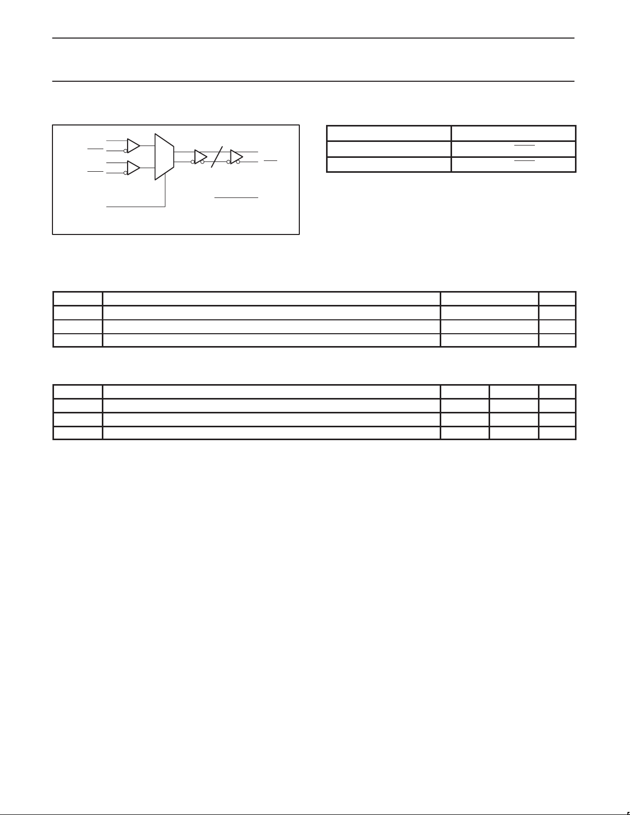
LOGIC SYMBOL
CLK0
CLK0
CLK1
CLK1
CLK_SEL
0
1
Figure 2. Logic symbol
10
V
BB
Q0:9
Q0:9
SW00908
ABSOLUTE MAXIMUM RATINGS
Absolute Maximum Ratings are those values beyond which damage to the device may occur. Functional operation under these conditions is not implied.
SYMBOL
V
Supply voltage –0.5 to +4.6 V
CC
ESDHBM Electrostatic discharge (Human Body Model; 1.5 kΩ, 100 pF) >2 kV
ESDMM Electrostatic discharge (Machine Model; 0 kΩ, 200 pF) >200 V
PARAMETER LIMITS UNIT
FUNCTION TABLE
CLK_SEL Active input
0 CLK0, CLK0
1 CLK1, CLK1
PCK111
RECOMMENDED OPERATING CONDITIONS
SYMBOL PARAMETER MIN MAX UNIT
T
V
V
amb
Supply voltage 2.375 3.8 V
CC
Receiver input voltage V
IR
EE
Operating ambient temperature range in free air –40 +85 °C
V
CC
V
2001 Sep 07
3
 Loading...