


INTEGRATED CIRCUITS
DATA SH EET
PCF8833
STN RGB - 132 × 132 × 3 driver
Objective specification 2003 Feb 14

Philips Semiconductors Objective specification
STN RGB - 132 × 132 × 3 driver PCF8833
CONTENTS
1 FEATURES
2 GENERAL DESCRIPTION
3 ORDERING INFORMATION
4 BLOCK DIAGRAM
5 PINNING
6 INSTRUCTIONS
6.1 Exit commands
6.2 Function set
7 FUNCTIONAL DESCRIPTION
7.1 MPU interfaces
7.2 Display data RAM and access arbiter
7.3 Command decoder
7.4 Grey scale controller
7.5 Timing generator
7.6 Oscillator
7.7 Reset
7.8 LCD voltagegenerator and bias level generator
7.9 Column drivers, data processing and data
latches
7.10 Row drivers
8 PARALLEL INTERFACE
8.1 8080-series 8-bit parallel interface
9 SERIAL INTERFACE
9.1 Write mode
9.2 Read mode
10 LIMITING VALUES
11 HANDLING
12 DC CHARACTERISTICS
13 AC CHARACTERISTICS
14 APPLICATION INFORMATION
14.1 Supply and capacitor connection configuration
15 MODULE MAKER PROGRAMMING
15.1 V
calibration
LCD
15.2 Factory defaults
15.3 Seal bit
15.4 OTP architecture
15.5 Interface commands
15.6 Suggestion on how to calibrate V
LCD2
using
MMVOP
15.7 Example of filling the shift register
15.8 Programming flow
15.9 Programming specification
16 INTERNAL PROTECTION CIRCUITS
17 BONDING PAD INFORMATION
18 TRAY INFORMATION
19 DATA SHEET STATUS
20 DEFINITIONS
21 DISCLAIMERS
2003 Feb 14 2

Philips Semiconductors Objective specification
STN RGB - 132 × 132 × 3 driver PCF8833
1 FEATURES
• Single chip LCD controller and driver
• 132 rows and 396 column outputs (132 × RGB)
• Low cross talk by Frame Rate Control (FRC)
• 4 kbyte colours (RGB) = 4 : 4 : 4 mode
• 256 colours (RGB) = 3:3:2 mode using the 209 kbit
RAM and a Look-Up Table (LUT)
• 65 kbyte colours (RGB) = 5 : 6 : 5 mode using the
209 kbit RAM with dithering
• 8 colours Power-save mode
• Display data RAM 132 × 132 (RGB) (4 kbyte colour)
• Interfaces:
– 3-line serial interface
– 8-bit 8080 Intel CPU interface.
• Display features:
– Area scrolling
– 32-line partial Display mode
– Software programmable colour depth mode
– N-line inversion for low cross talk.
• On-chip:
– Oscillator for display system, requires no external
components (external clock also possible)
– Generation of V
– Segmented temperature compensation of V
LCD
LCD
and
frame frequency.
• Logic supply voltage range V
DD1
to V
SS1
:
– 1.5 to 3.3 V.
• Analog supply voltage range for V
to V
SS2
:
generation V
LCD
DD2
– 2.4 to 4.5 V.
• Analog supply voltage range for reference voltage
generation V
DD3
to V
SS1
:
– 2.4 to 3.5 V.
• Display supply voltage range V
LCD
to V
SS1
:
– 3.8 to 20 V.
• Low power consumption; suitable for battery operated
systems
• CMOS compatible inputs
• Manufactured in silicon gate CMOS process
• Optimized layout for COF, Chip On Glass (COG) and
Transformer Coupled Plasma (TCP) assembly.
2 GENERAL DESCRIPTION
The PCF8833 is a single chip low power CMOS LCD
controller driver, designed to drive colour Super-Twisted
Nematic (STN) displays of 132 rows and 132 RGB
columns. All necessary functions for the display are
provided in a single chip, includingdisplay RAMwhich has
a capacity of 209 kbit (132 × 12-bit × 132). The PCF8833
uses the Multiple Row Addressing (MRA) driving
technique in order toachieve thebest opticalperformance
at the lowest power consumption. The PCF8833 offers
2 types of microcontroller interfaces namely the
8080 system interface and the 3-line serial interface.
3 ORDERING INFORMATION
PACKAGE
TYPE NUMBER
NAME DESCRIPTION VERSION
PCF8833U/2DA/1 − chip with bumps in tray −
2003 Feb 14 3
Philips Semiconductors Objective specification
STN RGB - 132 × 132 × 3 driver PCF8833
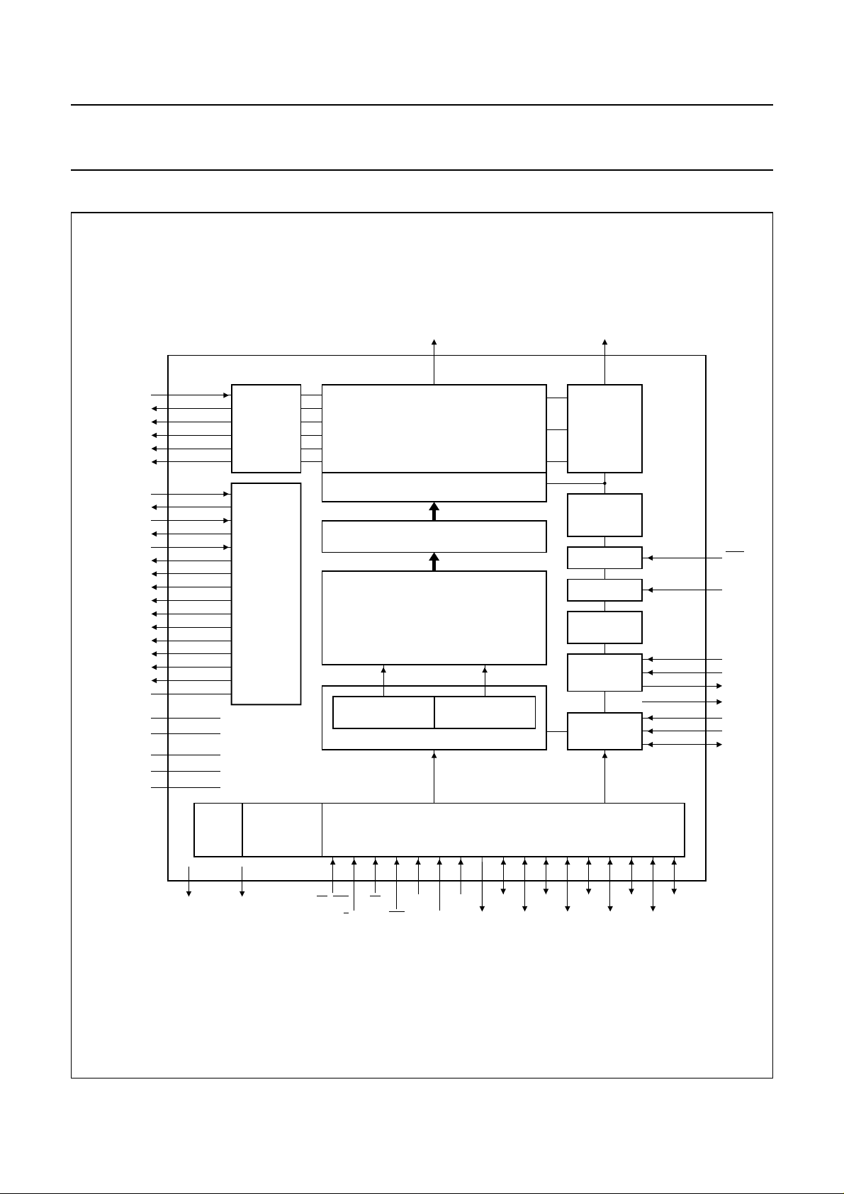
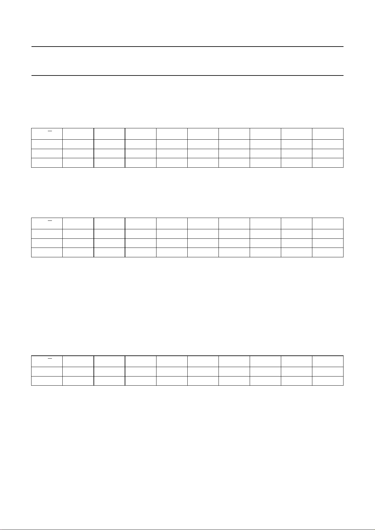
4 BLOCK DIAGRAM
handbook, full pagewidth
V
LCDIN2
V2H
V1H
VC
V1L
V2L
V
LCDSENSE
V
LCDOUT1
V
LCDIN1
V
LCDOUT2
V
DD2
C1+
C1−
C2+
C2−
C3+
C3−
C4+
C4−
C5+
C5−
V
SS2
V
OTP(gate)
V
OTP(drain)
V
DD3
V
DD1
V
SS1
713, 719
731, 732
729, 730
724 to 728
722, 723
720, 721
712
674 to 683
684 to 690
703 to 711
530 to 539
626 to 631
632 to 637
638 to 643
644 to 649
650 to 655
656 to 661
662 to 667
668 to 673
691 to 696
697 to 702
508 to 517
565 to 572
557 to 564
525 to 529
519 to 524
498 to 507
LCD BIAS
LEVEL
GENERATOR
LCD
VOLTAGE
GENERATOR
X AND Y RAM WRITE
ADDRESS COUNTER
PCF8833
C0 to C395
34 to 429
COLUMN DRIVERS
DATA PROCESSING
DATA LATCHES
DISPLAY DATA RAM
132 × 132 × 12-bits
DISPLAY ADDRESS
READ COUNTER
ARBITER
R0 to R131
2 to 33, 430 to 461,
464 to 495, 733 to 768
ROW
DRIVERS
ORTHOGONAL
FUNCTION
GENERATOR
RESET
OSCILLATOR
TIMING
GENERATOR
GREYSCALE
CONTROLLER
COMMAND
DECODER
496
555
578
577
576
575
574
573
625
RES
OSC
T1
T2
T3
T4
T5
T6
T7
256/64 KBYTES
256
COLOUR
LUT
V
DD(tieoff)VSS(tieoff)
TO 4 KBYTES
COLOUR
MAPPING
579, 624 518 549 551 550 552 553 554 548 547 545 543 541 546 544 542 540 497556
CS/SCE RD
D/C/SCLK WR
PS0
Fig.1 Block diagram.
2003 Feb 14 4
MPU INTERFACES
PS2
PS1
SDOUT
D0/SDIND1D2
D4 TE
D3
D6
D5
D7
MGU910

Philips Semiconductors Objective specification
STN RGB - 132 × 132 × 3 driver PCF8833
5 PINNING
SYMBOL PAD TYPE DESCRIPTION
R95 to R64 2 to 33 O LCD row driver outputs
C0 to C395 34 to 429 O LCD column driver outputs
R0 to R31 430 to 461 O LCD row driver outputs
R63 to R32 464 to 495 O LCD row driver outputs
RES 496 I external reset; this signal will reset the device and must be applied to properly
initialize the chip (active LOW)
TE 497 O/I tearing line (in Normal mode it is always an output)
V
SS1
V
SS2
CS/SCE 518 I chip select parallel interface or serial chip enable (active LOW)
V
DD1
V
DD3
V
DD2
D7 540 I/O 8-bit parallel data; in Serial mode tie to V
D3 541 I/O 8-bit parallel data; in Serial mode tie to V
D6 542 I/O 8-bit parallel data; in Serial mode tie to V
D2 543 I/O 8-bit parallel data; in Serial mode tie to V
D5 544 I/O 8-bit parallel data; in Serial mode tie to V
D1 545 I/O 8-bit parallel data; in Serial mode tie to V
D4 546 I/O 8-bit parallel data; in Serial mode tie to V
D0/SDIN 547 I/O 8-bit parallel data or serial data input
SDOUT 548 O serial data output; in Parallel mode tie to V
D/
C/SCLK 549 I data/command indicator parallel interface or serial clock
WR 550 I write clock parallel interface; in Serial mode tie to V
RD 551 I read clock parallel interface; in Serial mode tie to V
PS0 552 I set serial or parallel interface mode PS1 and PS2 must tied to either V
PS1 553 I set serial or parallel interface mode PS1 and PS2 must tied to either V
PS2 554 I set serial or parallel interface mode PS1 and PS2 must tied to either V
498 to 507 PS system ground
508 to 517 PS system ground
519 to 524 PS logic supply voltage
525 to 529 PS V
530 to 539 PS
DD2
and V
are the supply voltage pins for the internal voltage generator
DD3
including the temperature compensation circuits; V
connected together but in this case care must be taken to respect the supply
voltage range (see Chapter 13); V
chip. V
can be connected together with V
DD1
must also be taken to respect the supply voltage range; see Chapter 13. V
and V
must not be applied before V
DD3
If the internal voltage generator is not used, pins V
connected to V
V
DD1
V
DD1
V
DD1
DD1
and V
DD2
is used as the supply for the rest of the
DD1
and V
DD2
DD1.
DD2
DD3
and V
can be
DD3
but in this case care
DD2
must be
DD3
.
or V
SS1
SS1
SS1
SS1
SS1
SS1
SS1
DD1
or V
or V
or V
or V
or V
or V
, V
DD1
DD1
DD1
DD1
DD1
DD1
DD1
or D0
SS1
DD1
(active LOW)
DD1
(active LOW)
SS1
SS1
SS1
or
or
or
2003 Feb 14 5

Philips Semiconductors Objective specification
STN RGB - 132 × 132 × 3 driver PCF8833
SYMBOL PAD TYPE DESCRIPTION
OSC 555 I oscillator input or external oscillator resistor connection; when the on-chip
oscillator is used this input must be connected to V
if used, is connected to this input and the internal oscillatormust be switched off
with a software command; if the oscillator and external clock are all inhibited by
connecting pin OSC to V
, the display is not clocked and may be left in a
SS1
DC state; to avoid this the chip should always be put into Power-down mode
before stopping the clock.
V
DD(tieoff)
V
OTP(drain)
V
OTP(gate)
556 O can be used to tie inputs to V
DD1
557 to 564 PS supply voltage for OTP programming (write voltage), in Application mode must
be tied to V
or left open-circuit
SS1
565 to 572 PS supply voltage for OTP programming, in Application mode must be tied to V
or left open-circuit
T6 573 I test pin; not accessible to user; must be connected to V
T5 574 I test pin; not accessible to user; must be connected to V
T4 575 O test pin; not accessible to user; must be left open-circuit
T3 576 O test pin; not accessible to user; must be left open-circuit
T2 577 I/O test pin; not accessible to user; must be also connected to V
T1 578 I/O test pin; not accessible to user; must be also connected to V
V
SS(tieoff)
V
SS(tieoff)
579 O can be used to tie inputs to V
624 O can be used to tie inputs to V
SS1
SS1
T7 625 I/O test pin; not accessible to user; must be connected to V
C1+ 626 to 631 I positive input pump capacitor voltage multiplier 1
C1− 632 to 637 I negative input pump capacitor voltage multiplier 1
C2+ 638 to 643 I positive input pump capacitor voltage multiplier 1
C2− 644 to 649 I negative input pump capacitor voltage multiplier 1
C3+ 650 to 655 I positive input pump capacitor voltage multiplier 1
C3− 656 to 661 I negative input pump capacitor voltage multiplier 1
C4+ 662 to 667 I positive input pump capacitor voltage multiplier 1
C4− 668 to 673 I negative input pump capacitor voltage multiplier 1
V
LCDOUT1
V
LCDIN1
674 to 683 O output voltage multiplier 1
684 to 690 PS LCD supply input voltage 1
C5+ 691 to 696 I positive input pump capacitor voltage multiplier 2
C5− 697 to 702 I negative input pump capacitor voltage multiplier 2
V
LCDOUT2
V
LCDSENSE
V
LCDIN2
703 to 711 O output voltage multiplier 2
712 I voltage multiplier regulation input; must be connected to V
713 to 719 PS LCD supply input voltage 2
V2L 720, 721 O LCD bias level
V1L 722, 723 O LCD bias level
VC 724 to 728 O LCD bias level
V1H 729, 730 O LCD bias level
; an external clocksignal,
DD1
SS1
SS1
SS1
SS1
SS1
LCDOUT2
SS1
2003 Feb 14 6

Philips Semiconductors Objective specification
STN RGB - 132 × 132 × 3 driver PCF8833
SYMBOL PAD TYPE DESCRIPTION
V2H 731, 732 O LCD bias level
R96 to R131 733 to 768 O LCD row driver outputs
Dummy 1,462,463,
580 to623,
769
6 INSTRUCTIONS
The PCF8833 communicates with the host using an 8-bit parallel interface or a 3-line serial interface. Processing of
instructions and data sent to the interface do not require the display clock. The display clock and interface clock are
independent from each other. The display clock is derived from the built-in oscillator.
The PCF8833 has 2 types of accesses; those defining the operating mode of the device (instructions) and those filling
the display RAM. Since writing to the RAM occurs more frequently, efficient data transfer is achieved by
autoincrementing the RAM address pointers.
There are 3 types of instructions:
1. For defining display configuration
2. For setting X and Y addresses
3. Miscellaneous.
Commands inthe range of 00Hto AFH not definedin Table 1 and commandDDH have the sameeffect as no operation
(NOP).
All commands in range B0H to B9H and DEH to FFH are forbidden.
2003 Feb 14 7

This text is here in white to force landscape pages to be rotated correctly when browsing through the pdf in the Acrobat reader.This text is here in
_white to force landscape pages to be rotated correctly when browsing through the pdf in the Acrobat reader.This text is here inThis text is here in
white to force landscape pages to berotated correctly when browsingthrough the pdf in the Acrobat reader. white toforce landscape pages tobe ...
2003 Feb 14 8
2003 Feb 14 8
Table 1 Command table; note1
D/C 7 6 5 4 3 2 1 0 DEFAULT OTP DESCRIPTION SECTION
00000000 0 00H−no operation (NOP)
00000000 1 01H−software reset (SWRESET) 6.2.3
00000001 0 02H−booster voltage off (BSTROFF) 6.2.4
00000001 1 03H−booster voltage on (BSTRON) 6.2.5
00000010 0 04H−read display identification
(RDDIDIF)
00000100 1 09H−read display status (RDDST) 6.2.7
00001000 0 10H−Sleep_IN 6.2.8
00001000 1 11H−Sleep_OUT 6.2.9
00001001 0 12H−Partial mode on (PTLON) 6.2.10
00001001 1 13H−normal Display mode on
(NORON)
00010000 0 20H−display inversion off (INVOFF) 6.2.12
00010000 1 21H−display inversion on (INVON) 6.2.13
00010001 0 22H−all pixel off (DALO)
00010001 1 23H−all pixel on (DAL)
00010010 1 25H−set contrast (SETCON) 6.2.16
1 X VCON6VCON5VCON4VCON3VCON2VCON1VCON
00010100 0 28H−display off (DISPOFF) 6.2.17
00010100 1 29H−display on (DISPON) 6.2.18
00010101 02AH−column address set (CASET) 6.2.19
1 xs[7] xs[6] xs[5] xs[4] xs[3] xs[2] xs[1] xs[0] 02H − X address start; 0 ≤xs ≤ 83H
1 xe[7] xe[6] xe[5] xe[4] xe[3] xe[2] xe[1] xe[0] 81H − X address end; xs ≤ xe ≤ 83H
00010101 12BH−page address set (PASET) 6.2.20
1 ys[7] ys[6] ys[5] ys[4] ys[3] ys[2] ys[1] ys[0] 02H − Y address start; 0 ≤ys ≤ 83H
1 ye[7] ye[6] ye[5] ye[4] ye[3] ye[2] ye[1] ye[0] 81H − Y address end; ys ≤ ye ≤ 83H
00010110 02CH−memory write (RAMWR) 6.2.21
1D7D6D5D4D3D2D1 D0 XXH−write data 6.2.21
00010110 12DH−colour set (RGBSET) 6.2.22
1 X X X X R3 R2 R1 R0 00H − red tone 000 6.2.22
1 6 bytes for 6 red tones − 6 red tones 6.2.22
00H − set contrast
0
6.2.1
6.2.6
6.2.11
6.2.14
6.2.15
6.2.16
6.2.19
6.2.19
6.2.20
6.2.20
Philips Semiconductors Objective specification
Philips Semiconductors Objective specification
STN RGB - 132 × 132 × 3 driver PCF8833
STN RGB - 132 × 132 × 3 driver PCF8833

This text is here in white to force landscape pages to be rotated correctly when browsing through the pdf in the Acrobat reader.This text is here in
_white to force landscape pages to be rotated correctly when browsing through the pdf in the Acrobat reader.This text is here inThis text is here in
white to force landscape pages to berotated correctly when browsingthrough the pdf in the Acrobat reader. white toforce landscape pages tobe ...
2003 Feb 14 9
2003 Feb 14 9
C 7 6 5 4 3 2 1 0 DEFAULT OTP DESCRIPTION SECTION
D/
1 X X X X R3 R2 R1 R0 0FH − red tone 111 6.2.22
1 X X X X G3 G2 G1 G0 00H − green tone 000 6.2.22
1 6 bytes for 6 green tones − 6 green tones 6.2.22
1 X X X X G3 G2 G1 G0 0FH − green tone 111 6.2.22
1 X X X X B3 B2 B1 B0 00H − blue tone 00 6.2.22
1 2 bytes for 2 blue tones − 2 blue tones 6.2.22
1 X X X X B3 B2 B1 B0 0FH − blue tone 11 6.2.22
00011000 0 30H−partial area (PTLAR) 6.2.23
1 AA1S7 AA1S6 AA1S5 AA1S4 AA1S3 AA1S2 AA1S1 AA1S0 00H − PTLAR active area start address
1 AA1E7 AA1E6 AA1E5 AA1E4 AA1E3 AA1E2 AA1E1 AA1E1 1FH − PTLAR active area end address
00011001 1 33H−vertical scroll definition
(VSCRDEF)
1TF
1SA
1BF
7TF6
7SA6
7BF6
TF
SA
BF
TF
5
SA
5
BF
5
TF
4
SA
4
BF
4
TF
3
SA
3
BF
3
TF
2
2
2
SA
BF
1
1
1
TF
SA
BF
0
0
0
00H − top fixed area 6.2.24
82H − scroll area 6.2.24
00H − bottom fixed area 6.2.24
00011010 0 34H−tearing line off (TEOFF) 6.2.25
00011010 1 35H−tearing line on (TEON) 6.2.26
1XXXXXXX X 00H− 6.2.26
00011011 0 36H−memory data access control
(MADCTL)
1 MY MX V LAO RGB X X X 00H − RAM data addressing/data
control
00011011 1 37H−set Scroll Entry Point (SEP)
1 SEP7 SEP6 SEP5 SEP4 SEP3 SEP2 SEP1 SEP0 00H − scroll entry point
00011100 0 38H−Idle mode off (IDMOFF)
00011100 1 39H−Idle mode on (IDMON)
00011101 03AH−interface pixelformat (COLMOD)
1 X X X X X P2 P1 P0 03H − colour interface format
(2)
0 1 0 1 1 0 0 0 0 B0H x
1 X X X X VPR
1 X X X VPR
VPR
4
VPR
8
VPR
3
VPR
7
VPR
2
VPR
6
1
VPR
5
0
08H x V
01H x V
set VOP(SETVOP)
OP
OP
0 1 0 1 1 0 1 0 BRS B4H x Bottom Row Swap (BRS)
6.2.23
6.2.23
6.2.24
6.2.27
6.2.27
6.2.24
6.2.24
6.2.28
6.2.29
6.2.30
6.2.30
6.2.31
6.2.31
6.2.31
6.2.32
Philips Semiconductors Objective specification
Philips Semiconductors Objective specification
STN RGB - 132 × 132 × 3 driver PCF8833
STN RGB - 132 × 132 × 3 driver PCF8833

This text is here in white to force landscape pages to be rotated correctly when browsing through the pdf in the Acrobat reader.This text is here in
_white to force landscape pages to be rotated correctly when browsing through the pdf in the Acrobat reader.This text is here inThis text is here in
white to force landscape pages to berotated correctly when browsingthrough the pdf in the Acrobat reader. white toforce landscape pages tobe ...
2003 Feb 14 10
2003 Feb 14 10
C 7 6 5 4 3 2 1 0 DEFAULT OTP DESCRIPTION SECTION
D/
0 1 0 1 1 0 1 1 TRS B6H x Top Row Swap (TRS)
0 1 0 1 1 1 0 0 FINV B9H − super Frame INVersion (FINV)
0 1 0 1 1 1 0 1 DOR BAH − Data ORder (DOR)
0 1 0 1 1 1 1 0 TCDFE BDH − enable/disable DF temp comp
(TCDFE)
0 1 0 1 1 1 1 1 TCVOPE BFH − enable or disable V
OP
temp
comp (TCVOPE)
0 1 1 0 0 0 0 0 EC C0H − Internal or external oscillator
(EC)
0 1 1 0 0 0 0 1 0 C2H x set multiplication factor
(SETMUL)
1 X X X X X X S1 S0 03H x multiplication factor
0 1 1 0 0 0 0 1 1 C3H x set TCVOP slopes A and B
(TCVOPAB)
1 X SLB
SLB
2
SLB
1
0
X SLA
SLA
2
SLA
1
0
34H x
0 1 1 0 0 0 1 0 0 C4H x set TCVOP slopes C and D
(TCVOPCD)
1 X SLD
SLD
2
SLD
1
0
X SLC
SLC
2
SLC
1
0
75H x
0 1 1 0 0 0 1 0 1 C5H x set divider frequency (TCDF)
1 X DFA
1 X DFB
1 X DFC
1 X DFD
DFA
6
DFB
6
DFC
6
DFD
6
DFA
5
DFB
5
DFC
5
DFD
5
DFA
4
DFB
4
DFC
4
DFD
4
DFA
3
DFB
3
DFC
3
DFD
3
DFA
2
DFB
2
DFC
2
DFD
2
DFA
1
1
1
1
DFB
DFC
DFD
0
0
0
0
56H x set divider factor in region A
35H x set divider factor in region B
30H x set divider factor in region C
25H x set divider factor in region D
0 1 1 0 0 0 1 1 0 C6H x set divider frequency 8-colour
mode (DF8colour)
1 X DF8
DF8
6
DF8
5
DF8
4
DF8
3
DF8
2
DF8
1
0
35H x set divider factor in 8-colour
mode
0 1 1 0 0 0 1 1 1 C7H x set bias system (SETBS)
1X X X XVB
3VB2
VB
1
VB
0
0BH x bias systems
01100100 0C8H−temperature read back
(RDTEMP)
01100100 1C9H−N-Line Inversion (NLI)
1 NLI
NLI
7
NLI
6
NLI
5
NLI
4
NLI
3
NLI
2
NLI
1
0
13H x after NLI time slots inversion
0 1 1 0 1 1 0 1 0 DAH x read ID1 (RDID1)
6.2.33
6.2.34
6.2.35
6.2.36
6.2.37
6.2.38
6.2.39
6.2.39
6.2.40
6.2.40
6.2.40
6.2.40
6.2.41
6.2.41
6.2.41
6.2.41
6.2.41
6.2.42
6.2.42
6.2.43
6.2.43
6.2.44
6.2.45
6.2.45
6.2.46
Philips Semiconductors Objective specification
Philips Semiconductors Objective specification
STN RGB - 132 × 132 × 3 driver PCF8833
STN RGB - 132 × 132 × 3 driver PCF8833
This text is here in white to force landscape pages to be rotated correctly when browsing through the pdf in the Acrobat reader.This text is here in
_white to force landscape pages to be rotated correctly when browsing through the pdf in the Acrobat reader.This text is here inThis text is here in
white to force landscape pages to berotated correctly when browsingthrough the pdf in the Acrobat reader. white toforce landscape pages tobe ...
2003 Feb 14 11
2003 Feb 14 11
C 7 6 5 4 3 2 1 0 DEFAULT OTP DESCRIPTION SECTION
D/
0 1 1 0 1 1 0 1 1 DBH x read ID2 (RDID2)
0 1 1 0 1 1 1 0 0 DCH x read ID3 (RDID3)
0 1 1 1 0 1 1 1 SFD EFH x select factory defaults
01111000 0 F0H−enter Calibration mode
1 X X ORA
01111000 1 F1H−shift data in OTP shift registers
1 OS7 OS6 OS5 OS4 OS3 OS2 OS1 OS0 XX − multiple data byte; any number
Notes
1. X = don’t care.
2. This function can be set by OTP.
3. If the OTP bit Enable Factory Defaults (EFD) has been programmed to logic 1 (default value is logic 0), then the Set Factory Defaults (SFD)
instruction is ignored and the device will always use the OTP default data.
ORA1ORA
2
X OPE CALMM 00H − set calibration control settings
0
(OTPSHTIN)
of bytes allowed
(3)
6.2.46
6.2.46
6.2.47
15.5
15.5
15.5
15.5
Philips Semiconductors Objective specification
Philips Semiconductors Objective specification
STN RGB - 132 × 132 × 3 driver PCF8833
STN RGB - 132 × 132 × 3 driver PCF8833

Philips Semiconductors Objective specification
STN RGB - 132 × 132 × 3 driver PCF8833
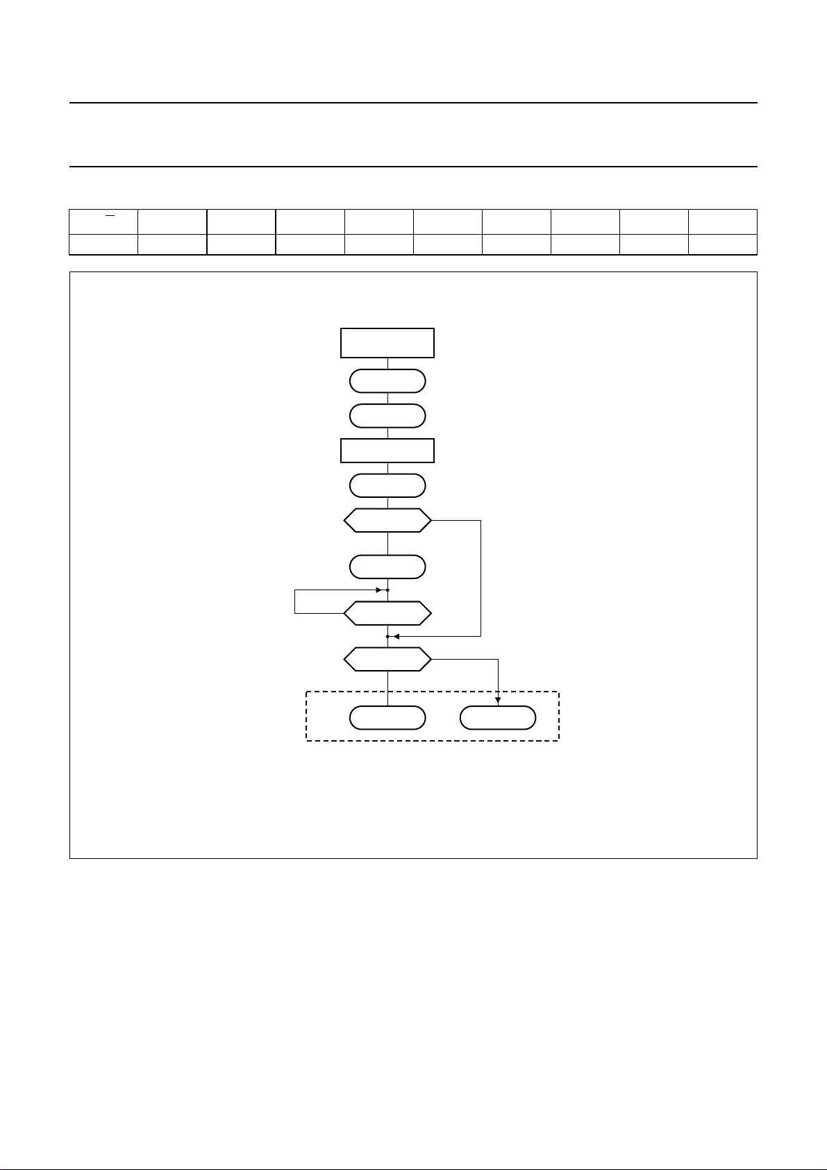
6.1 Exit commands Table 2 Command description
INPUT
COMMAND
Sleep_IN
(SLPIN)
Sleep_OUT
(SLPOUT)
BSTROFF display voltage generation off display is switched on or off by
BSTRON display voltage generation on display is switched on or off by
DISPOFF display off rows and columns are tied to V
DISPON display on DISPOFF
NORON Normal mode on full display is driven by RAM data PTLON SEP
PTLON Partial mode on partial display area is driven by RAM
SEP Scroll mode on NORON
PIXON (DAL) in full Display mode (NORON) all pixels
PIXOFF
(DALO)
IDMOFF Idle mode off full colour resolution storedin theRAM is
IDMON Idle mode on 8-colour mode became active: The MSB
INVOFF inverted display off INVON
INVON inverted display on in Partial mode only pixels of partial area
TEOFF tearing pulse disabled TEON
TEON tearing pulse enabled TEOFF reset
Power-down mode: power-downhas priority over display and
display off
display voltage generation off
exit power-down: after reset; BSTRONand DISPONis set,
display → DISPON/DISPOFF
display voltage
generation → BSTRON/BSTROFF
(refresh from OTP cells if CALMM = 0)
are on; in partial Display mode only
partial area pixels are driven on; pixels
outside partial area are off
all pixel off command INVON is not effective when
PARAMETERS CONDITIONS
booster settings, but the setting is kept
but become active only with Sleep_OUT
DISPON/DISPOFF
DISPON/DISPOFF
SS1
data; display area outside partial area is
off
command INVON is not effective when
DAL is active
DALO is active
written to the display
of data stored in RAM is evaluated only
are inverted; INVON is not effective;
when DAL or DALO are active
EXIT
COMMAND
Sleep_OUT
Sleep_IN reset
BSTRON reset
BSTROFF
DISPON reset
NORON SEP
reset
PTLON reset
PIXOFF
(DALO)
NORON
PTLON SEP
reset
PIXON (DAL)
NORON
PTLON SEP
reset
IDMON
IDMOFF reset
INVOFF reset
2003 Feb 14 12
Philips Semiconductors Objective specification
STN RGB - 132 × 132 × 3 driver PCF8833
6.2 Function set
6.2.1 NO OPERATION No operation (NOP) has no effect on internal data or settings. However, it can be used to terminate data transfer (read
and write).
Table 3 No operation command bits
D/C76543210DEFAULT
00000000000H
6.2.2 RESET The PCF8833 has ahardware and a software reset. After
power-upa hardwarereset(pin RES)mustbe applied;see
Fig.50. The hardware and software resets give the same
results. After a reset, the chip has the following state:
• All LCD outputs are set to VSS (display off)
• RAM data unchanged
• Power-down mode (Sleep_IN)
• Command register set to default states; see Table 4
• Interface pins are set to inputs.
Table 4 Reset state after hardware and software reset
COMMAND DESCRIPTION RESET STATE
Sleep_IN PCF8833 is in Sleep_IN mode (booster and display are switched off) −
INVOFF display inversion is off −
BSTRON when Sleep_OUT is active; booster is switched on −
DISPON when Sleep_OUT is active; display is turned on −
TEOFF tearing effect line pulse is turned off −
IDMOFF Idle mode is turned off (4 kbyte colour mode, not 8-colour mode) −
NORON Normal mode is active, not Scroll or Partial mode −
V RAM write in X direction 0
MY no mirror Y 0
RGB colour order is RGB 0
MX no mirror X 0
LAO line address order (top to bottom) 0
BRS bottom rows are not mirrored; note 1 0
TRS top rows are not mirrored; note 1 0
FINV super frame inversion is on 1
DOR normal data order 0
TCDFE DF temperature compensation switched on 1
TCVOPE VOP temperature compensation switched on 1
EC internal oscillator 0
After a reset, care mustbe taken with respect to the reset
timing constraints (see Fig.50) when the PCF8833 is
powered-up. The power-up must be done by sending the
Sleep_OUT command.
After a power-up the display RAM content is undefined.
Neither a hardware reset nor asoftware resetchanges the
data that is stored in the display RAM. Sending display
data must stop 160 ns before issuing a hardware reset,
otherwise thelast word writtento the displayRAM may be
corrupted. The row and column outputs are tied to V
with a reset because power-down (Sleep_IN) is in the
reset state.
SS1
2003 Feb 14 13

Philips Semiconductors Objective specification
STN RGB - 132 × 132 × 3 driver PCF8833
COMMAND DESCRIPTION RESET STATE
xs[7:0] x address start 2DEC
xe[7:0] x address end 129DEC
ys[7:0] y address start 2DEC
ye[7:0] y address end 129DEC
RGBSET 256 to 4 kbyte colour LUT see Section 6.2.22
AA1S[7:0] partial area start address 0DEC
AA1E[7:0] partial area end address 31DEC
TF[7:0] top fixed area 0DEC
SA[7:0] scroll area 130DEC
BF[7:0] bottom fixed area 0DEC
SEP[7:0] scroll entry point 0DEC
P[2:0] interface pixel format is 12-bit/pixel 011
VPR[8:0] programming of V
S[1:0] charge pump multiplication factor; note 1 11
SLA[2:0] select slope for segment A; note 1 100
SLB[2:0] select slope for segment B; note 1 011
SLC[2:0] select slope for segment C; note 1 101
SLD[2:0] select slope for segment D; note 1 111
DFA[6:0] frame frequency for segment A is 80 Hz; note 1 56DEC
DFB[6:0] frame frequency for segment B is 130 Hz; note 1 35DEC
DFC[6:0] frame frequency for segment C is 150 Hz; note 1 30DEC
DFD[6:0] frame frequency for segment D is 180 Hz; note 1 25DEC
DF8[6:0] frame frequency for 8-colour mode is 130 Hz; note 1 35DEC
VB[3:0] bias system is F/G
NLI[7:0] inversion is after 19 time slots (76 rows in Full mode); note 1 19DEC
VCON[6:0] no contrast setting is set (twos complement number); note 1 0DEC
SFD OTP programmed data is used; note 1 1
CALMM not in Calibration mode 0
OPE disable OTP programming voltage; note 2 0
ORA[2:0] OTP row address selection 000
voltage; note 1 257DEC
LCD2
= 2.5; note 1 1011
max
Notes
1. These values can be set by the module maker. If the factory defaults OTP bit EFD have been set, the value cannot
be changed via the interface. Otherwise, the OTP data will be used if SFD is set to logic 1, which is the reset state.
2. Calibration modemay notbe entered ifthe SEAL bit has beenset. Programming isonly possiblewhen in Calibration
mode.
2003 Feb 14 14
Philips Semiconductors Objective specification
STN RGB - 132 × 132 × 3 driver PCF8833
6.2.3 SOFTWARE RESET
The software reset (SWRESET) has exactly the same effect as the hardware reset; see Section 6.2.2.
After sending SWRESET any command can be sent immediately without any additional delay in between, for instance:
Sleep_OUT, BSTRON and DISPON, etc.
Table 5 Software reset register bits
D/C76543210DEFAULT
00000000101H
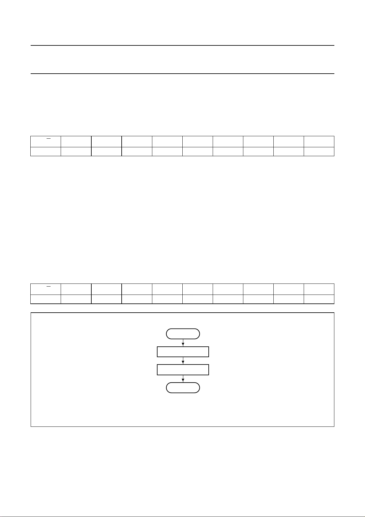
6.2.4 BOOSTER VOLTAGE OFF
The DC-to-DC converters are turned off and pins
V
LCDOUT1
and V
LCDOUT2
become 3-state.
In order to avoid any optical effect on the display, the
sequence given in Fig.2 must be used before the internal
display supply generation circuits are turned off.
The external LCD supply input voltages (V
V
) can be applied while the display voltage
LCDIN2
LCDIN1
and
Command Sleep_IN does not effect the setting of
BSTRON/BSTROFF or DISPON/DISPOFF, but switches
off the DC-to-DC converter (booster) and ties the display
outputs to V
SS1
.
For the effect of possible combinations of commands
Sleep_IN/Sleep_OUT and BSTRON/BSTROFF; see
Table 17 and Fig.4. Figure 7 shows the effects of the
combination of commands BSTRON and BSTROFF with
DISPON and DISPOFF.
generation (BSTROFF) is off. When BSTROFF, DISPON
and Sleep_OUT are set, the external LCD supply input
voltages (V
LCDIN1
and V
) must be applied, otherwise
LCDIN2
the display outputs will be undefined.
Table 6 Booster voltage off register bits
D/C76543210DEFAULT
00000001002H
handbook, halfpage
start
send DISPOFF (28H)
send BSTROFF (02H)
end
Fig.2 Booster voltage off flow chart.
2003 Feb 14 15
MGU911
Philips Semiconductors Objective specification
STN RGB - 132 × 132 × 3 driver PCF8833
6.2.5 BOOSTER VOLTAGE ON The LCD supply generation circuits will be switched on
whenthe Boostervoltage on(BSTRON) command issent.
The BSTRON commandhas a direct effect only whenthe
PCF8833 is not in Power-down mode (Sleep_OUT is not
active).
With a reset DISPON (see Section 6.2.18) and BSTRON
are set, the PCF8833 will start-up with Sleep_OUT (see
Section 6.2.7) following the built-in start-up sequence
which generates the requested voltages and switches on
the display, unless DISPOFF and/or BSTROFF was sent.
When theLCD supplygeneration circuits areswitched on,
it is necessary to wait for a certain time before the power
circuitsbecome stableand the displaycan beswitchedon.
Because this time is dependent on the required V
LCD
voltage,the externalcomponents used,the appliedsupply
voltage and some other parameters, the PCF8833
monitors the LCD supply generation circuit internally and
will only switch-on the display when the LCD supply
The status of the LCD supply generation circuits can be
monitored with the read display status (RDDST)
command; see Section 6.2.7.
Figure 3 shows two sequences for using the BSTRON
command, assuming BSTROFF and DISPOFF were set
before sending Sleep_OUT.In sequence A the command
to switch the display on (DISPON) issent to the PCF8833
before the BSTRON command is sent. Therefore the
display will only be switched on when the LCD supply
generation circuitgenerates a stable V
. Insequence B
LCD
the RDDST command is used to monitor the LCD supply
generation circuit and, after the D31 bit of the RDDST is
set to logic 1, the DISPON command will be sent;
see Section 6.2.7.
For the effect of possible combinations of commands
Sleep_IN/Sleep_OUT and BSTRON/BSTROFF; see
Table 17 and Fig.4. Figure 7 shows the effects of the
combination of commands BSTRON and BSTROFF with
DISPON and DISPOFF.
generation circuits are stable.
Table 7 Booster voltage on register bits
D/C76543210DEFAULT
00000001103H
handbook, full pagewidth
LCD will be switched on
start
send Sleep_OUT 11H
send DISPON 29H
send BSTRON 03H
when LCD supply
generation circuit
is stable
end
sequence A
Fig.3 Booster voltage on flow charts.
2003 Feb 14 16
start
send Sleep_OUT 11H
send BISTRON 03H
monitor D[31
RDDST 09H
send DISPON 29H
sequence B
]
D31 = 1
end
D31 = 0
MGU912
Philips Semiconductors Objective specification
STN RGB - 132 × 132 × 3 driver PCF8833
6.2.6 READ DISPLAY IDENTIFICATION INFORMATION The Read Display Identification Information (RDDIDIF)
command returns a 24-bit display identification
information. The identification information is valid only
5 ms after applying a hardware reset. Therefore the
RDDIDIF command should not be sent earlier than 5 ms
after a hardware reset.
The input andoutput data format is givenin Table 9. After
the command byte 04H is sent, the read starts with one
dummy clock cycle followed by the 3 status bytes (see
Fig.47).
Table 8 Read display identification information register bits
D/C76543210DEFAULT
0 0000010004H
Table 9 RDDIDIF data format for Serial mode
BIT D/
(S)DIN 0 0 0 0 0 0 1 0 0 04H
(S)DOUT − X (only one dummy clock cycle, not a full byte) X
(S)DOUT − D23 D22 D21 D20 D19 D18 D17 D16 45H
C76543210DEFAULT
− D15 D14 D13 D12 D11 D10 D9 D8 XX
− D7 D6 D5 D4 D3 D2 D1 D0 XX
When less than 25 read clock cycles are sent in Serial
mode, the identification information read must be
interrupted by a hardware reset or rising edge of SCE.
The definition of the display identification bits is given in
Table 11.
Table 10 RDDIDIF data format for Parallel mode
D/
C76543210DEFAULT
0 0000010004H
1 XXXXXXXXXX
1 D23 D22 D21 D20 D19 D18 D17 D16 45H
1 D15 D14 D13 D12 D11 D10 D9 D8 XX
1 D7D6D5D4D3D2D1D0 XX
Table 11 Description of the display identification bits
BIT BIT DESCRIPTION RD BYTE REMARK
D[23:16] manufacturer ID RDID1 hard wired = 45H
D15 driver/module ID
(STN B/W = 0 and
STN Colour = 1)
D[14:8] driver/module version ID
D[7:0] driver/module code RDID3
Note
1. RDID3 will be programmed in OTP cells. This ID can be set to 03H by the module maker.
RDID2 OTP programmed;
see Chapter 15
(1)
OTP programmed;
see Chapter 15
2003 Feb 14 17
Philips Semiconductors Objective specification
STN RGB - 132 × 132 × 3 driver PCF8833
6.2.7 READ DISPLAY STATUS The Read Display Status (RDDST) command returns a
32-bit display status information and can be accessed
when the PCF8833 is in normal Display mode (see
Section 6.2.11), in partial Display mode (see
Section 6.2.23) or in Sleep_IN mode; see Section 6.2.8.
The input and output data format is as follows: After the
command byte 09H is sent, the read starts with one
dummy clock cycle followed by the 4 status bytes (see
Fig.48).
Table 12 Read display status register bits
D/C76543210DEFAULT
00000100109H
Table 13 RDDST data format for Serial mode
BIT D/
(S)DIN 00000100109H
(S)DOUT − X (only one dummy clock cycle, not a full byte) XX
(S)DOUT − D31 D30 D29 D28 D27 D26 0 0 XX
C76543210DEFAULT
− 0 D22 D21 D20 D19 D18 D17 D16 XX
− D15 0 D13 D12 D11 D10 D9 0 XX
− 00000000XX
When less than 33 read clock cycles are sent in Serial
mode the status read must be interrupted by a hardware
reset or a rising edge of SCE.
The definition of the display statusbits isgiven inTable 11.
Table 14 RDDST data format for Parallel mode
D/C76543210DEFAULT
00000100109H
1 XXXXXXXXXX
1 D31 D30 D29 D28 D27 D26 0 0 XX
1 0 D22 D21 D20 D19 D18 D17 D16 XX
1 D15 0 D13 D12 D11 D10 D9 0 XX
100000000XX
2003 Feb 14 18

Philips Semiconductors Objective specification
STN RGB - 132 × 132 × 3 driver PCF8833
Table 15 Display identification bits description
BIT BIT DESCRIPTION STATUS
D31 booster voltage status logic 1 when BSTRON is selected and when the
LCD supply generation circuits are ready
logic 0 when BSTROFF is selected or when the
LCD supply generation circuits are not ready
D30 Yaddress order logic 1 when MY = 1
logic 0 when MY = 0
D29 X address order logic 1 when MX = 1
logic 0 when MX = 0
D28 vertical/horizontal addressing mode logic 1 when V = 1
logic 0 when V = 0
D27 line address order logic 1 when LAO = 1
logic 0 when LAO = 0
D26 RGB/BGR order logic 1 when RGB = 1
logic 0 when RGB = 0
D[25:23] no function, but can be read D[25:23] = 000
D[22:20] interface pixel format see Section 6.2.30
P2 = D22; P1 = D21 and P0 = D20
D19 Idle mode logic 1 when IDMON is selected
logic 0 when IDMOFF is selected
D18 Partial mode logic 1 when PTLON is selected
logic 0 otherwise
D17 Sleep_IN/OUT logic 1 when Sleep_OUT is selected
logic 0 when Sleep_IN is selected
D16 normal Display mode logic 1 when NORON is selected
logic 0 otherwise
D15 vertical Scroll mode logic 1 when SEP is selected
logic 0 otherwise
D14 no function; but can be read D14 = 0
D13 display inversion logic 1 when INVON is selected
logic 0 when INVOFF is selected
D12 all pixels on logic 1 when DAL is selected
logic 0 otherwise
D11 all pixels off logic 1 when DALO is selected
logic 0 otherwise
D10 display on/off logic 1 when DISPON is selected
logic 0 when DISPOFF is selected
D9 tearing effect line on/off logic 1 when TEON is selected
logic 0 when TEOFF is selected
D[8:0] no function; but can be read D[8:0] = 0:0000:0000
2003 Feb 14 19
Philips Semiconductors Objective specification
STN RGB - 132 × 132 × 3 driver PCF8833
6.2.8 SLEEP_IN By sending the Sleep_IN command, the PCF8833
immediatelyenters the Power-downmode,also referredto
as theSleep mode. In the Sleepmode the outputvoltages
of all LCD driver pins (rows and columns) are at V
SS1
(ground, all pixels are in off state), and the LCD supply
generation circuit and the oscillator are switched off. The
While in Sleep_IN mode all commands and data can be
sent and will be executed as in the Sleep_OUT state,
except some OTP related commands and temperature
readout related commands. In the Sleep_IN mode no
effect on the display can be seen.
The Sleep_IN mode is exited by command Sleep_OUT;
see Section 6.2.9.
Sleep_IN command does not change the state of the
DISPON/DISPOFF and BSTRON/BSTROFF commands,
but has the same effect as DISPOFF and BSTROFF;
see Table 17.
Table 16 Sleep_IN register bits
C76543210DEFAULT
D/
00001000010H
Table 17 Sleep_IN/OUT and BSTR_ON/OFF combination
BSTER_ON/BSTER_OFF Sleep_IN/Sleep_OUT
Booster
(1)
ON ON ON
ON OFF OFF
OFF ON OFF
OFF OFF OFF
Note
1. Booster is the built-in DC-to-DC converter also called voltage multiplier or charge pump.
6.2.9 SLEEP_OUT This command must be sent to allow the PCF8833 to
power-up (see Fig.4).
DISPON and BSTRON areset with a reset, the PCF8833
will start-up with Sleep_OUT followingthe built-in start-up
sequence which generates the requested voltages and
switches on the display, unless DISPOFF and/or
BSTROFF was sent after the last reset.
For the effects of possible combinations of commands
Sleep_IN/Sleep_OUT and BSTRON/BSTROFF; see
Table 17.
Figure 4 illustratesthe flow when sendingthe Sleep_OUT
command. The display is only switched on, when the
internally generated voltage V
is high enough.
LCD2
This time is self adapting and therefore dependent on
application conditions:
• It is longer for:
– Low V
DD2
– Higher resistors in supply wires and/or external
capacitors
– Higher external capacitors
– Higher required V
LCD2
voltage.
• Some other conditions, which may affect start-up time
are:
– Partial/full mode
– Selected bias system
– Temperature
– Selected temperature coefficients.
2003 Feb 14 20
Philips Semiconductors Objective specification
STN RGB - 132 × 132 × 3 driver PCF8833
Table 18 Sleep_OUT register bits
D/C76543210DEFAULT
00001000111H
handbook, full pagewidth
D31 = 0
ready
reset
HW or SW
Sleep_IN
D31 = 0
send Sleep_OUT
Sleep_OUT
booster
BSTRON
booster on
wait for D31 bit
D31 = 1
display
DISPON
display on display off
BSTROFF
DISPOFF
D31 is the booster voltage status bit; see Section 6.2.7.
Fig.4 Start-up, when leaving Power-down mode (i.e. after sending Sleep_OUT).
2003 Feb 14 21
MGU913
Philips Semiconductors Objective specification
STN RGB - 132 × 132 × 3 driver PCF8833
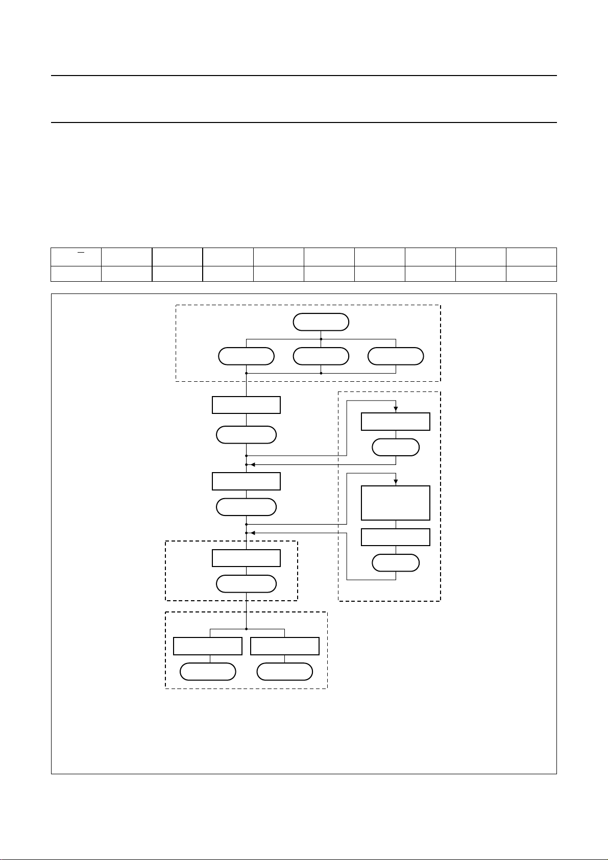
6.2.10 PARTIAL MODE ON
Partial mode on (PTLON) turns on the partial Display
mode.Only onepartialdisplay sizecanbe chosen.Normal
mode, Scroll mode, DALO and DAL are exited with this
command. When sending DAL after PTLON, only the
Anormal Displaymodecommand isusedto exitthe Partial
mode. Howthe partial displayarea can be programmed is
given in Section 6.2.23.
A sequence showing how the command PTLON can be
used is illustrated in Fig.5.
pixels of partial area are driven on.
Table 19 Partial mode on register bits
D/C76543210DEFAULT
00001001012H
handbook, full pagewidth
Initial state
(1)
Sleep_OUT
display on normal displaybooster on
send PTLAR
send DISPOFF
partial area def
display off
send PTLON
wait until
partial mode on
optional
send PTLAR
partial area def
exit partial mode
send NORON send SEP
normal display scroll mode
(1) If theinitial state is Sleep_IN, the same sequenceis valid, butSleep_OUT has to be sentto see theeffect on the display (afterdisplay voltage has
settled).
When sending DALafter PTLON, onlythe pixels ofpartial area are driven on. When sending INVON, in Partial mode only the pixels of partial area are
inverted. INVON is over-ruled by DAL and DALO. Pixels outside partial area always stay off.
display supply
voltage is settled
send DISPON
display on
optional
MGU914
Fig.5 Sequence how PTLON can be used.
2003 Feb 14 22

Philips Semiconductors Objective specification
STN RGB - 132 × 132 × 3 driver PCF8833
6.2.11 NORMAL DISPLAY MODE ON The normal Display mode on command (NORON) turns the display into Normal mode which is also the reset state. An explanation of how the command NORON can be used is illustrated in Fig.6.
Table 20 Normal Display mode on register bits
D/
CD7D6D5D4D3D2D1D0DEFAULT
00001001113H
6.2.12 D
ISPLAY INVERSION OFF
The Display inversionoff command (INVOFF) turns thedisplay into a non-inverted screen without modifying the display
data RAM. Display inversion off is the reset state of the PCF8833.
Table 21 Display inversion off register bits
C76543210DEFAULT
D/
00010000020H
6.2.13 D
ISPLAY INVERSION ON
The Displayinversion on command(INVON) turns thedisplay into an inverted screen without modifying the display data
RAM. The RAM data is read out and inverted while writing to the display.
The display Inversion mode can be switched off by sending the INVOFF command; see Section 6.2.12.
When sending INVON, in Partial mode only, the pixels of a partial area are inverted. INVON is overruled by DAL and
DALO. In Partial mode the pixels outside of the partial are always off.
Table 22 Display inversion on register bits
C76543210DEFAULT
D/
00010000121H
6.2.14 A
LL PIXELS OFF
The All pixels off command (DALO) can be switched off by sending the normal display on command (NORON) (see
Section 6.2.11) or by sending the partial Display mode on command (PTLON); see Section 6.2.10. Furthermore DALO
is left with the command DAL; see Section 6.2.15. When DALOis active all pixels are driven,as if the display RAM was
filled with all zeros (off-state). DALO does not change the data stored in the display RAM. Figure 6 illustrates how DAL
(all pixels on) and DALO (all pixels off) can be used.
All pixels will be switched off regardless of the display data RAM.
Table 23 All pixels off register bits
D/
C76543210DEFAULT
00010001022H
2003 Feb 14 23
Philips Semiconductors Objective specification
STN RGB - 132 × 132 × 3 driver PCF8833
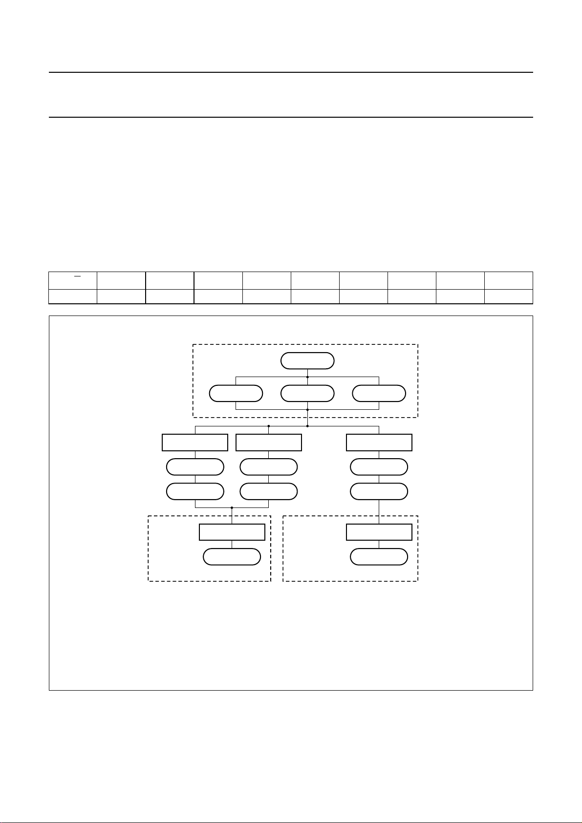
6.2.15 ALL PIXELS ON The All pixels on command (DAL) can be switched off by
sending the normal display on command (NORON); (see
Section 6.2.11) or by sendingthe partial Display mode on
command(PTLON); see Section 6.2.10.FurthermoreDAL
is left with thecommand DALO;see Section 6.2.14.When
DAL is active all pixels are driven, as if the display RAM
was filled with all ones (on-state). DAL does not change
When sending DAL after PTLON, only the pixels of the
partial areaare driven on.When sending INVON in Partial
mode only the pixels of the partial area are inverted.
INVON is over-ruled by DAL andDALO. Pixelsoutside the
partial are always off. Figure 6 illustrates how DAL (all
pixels on) and DALO (all pixels off) can be used.
All pixels will beswitched onregardless ofthe displaydata
RAM.
the data stored in the display RAM.
Table 24 All pixels on register bits
D/C76543210DEFAULT
00010001123H
handbook, full pagewidth
Initial state
(1)
Sleep_OUT
display on all pixel on/offbooster on
send SEP
exit pixel on/off
scroll mode on normal display partial mode on
send DAL/DALO
all pixel on/off
effect in
full display mode
(1) If theinitial stateis Sleep_IN, thesame sequenceis valid, but Sleep_OUThas to besent tosee the effect on the display (afterdisplay voltage
has settled).
When sending DAL after PTLON, only thepixels of partial area aredriven on. When sending INVON,in Partialmode only thepixels ofpartial area
are inverted. INVON is over-ruled by DAL and DALO. Pixels outside partial area always stay off.
send NORON
exit pixel on/off
effect in
partial display mode
send PTLON
exit pixel on/off
send DAL/DALO
all pixel on/off
MGU915
Fig.6 Flowchart representation of DAL and DALO.
2003 Feb 14 24

Philips Semiconductors Objective specification
STN RGB - 132 × 132 × 3 driver PCF8833
6.2.16 SET CONTRAST Usingthe Setcontrast command(SETCON) theV
ofthe VCON[6:0]register onthe V
programmingis explainedin Section 6.2.31.The VCON[6:0]is atwos complement
LCD
number; see Table 26. An overview over the complete programming range of V
voltageand thecontrast ofthe LCDcan beadjusted. The influence
LCD
can be found in Section 15.1.
LCD
Table 25 Set contrast register bits
D/C76543210DEFAULT
00010010125H
1 X VCON
VCON
6
VCON
5
VCON
4
VCON
3
VCON
2
VCON
1
00H
0
Table 26 Possible VCON values
VCON[6:0] DECIMAL EQUIVALENT V
OFFSET
LCD
0111111 63 2520 mV
0111110 62 2480 mV
0111101 61 2440 mV
:::
0000010 2 80 mV
0000001 1 40 mV
0000000 0 0 mV
1111111 −1 −40 mV
1111110 −2 −80 mV
:::
1000010 −62 −2480 mV
1000001 −63 −2520 mV
1000000 −64 −2560 mV
6.2.17 D
The Display off command (DISPOFF) connects all rows and columns to V
ISPLAY OFF
, i.e. all the pixels have a voltage of 0 V.
SS1
Since the reset state of the PCF8833 is Sleep_IN (see Section 6.2.8) the display will be in the off state after a reset.
The DISPOFF command can be switched off by sending the Display on command (DISPON); see Section 6.2.18.
Figure 7 shows the effects of the combination of commands BSTRON and BSTROFF with DISPON and DISPOFF.
Table 27 Display off register bits
D/
C76543210DEFAULT
00010100028H
6.2.18 D
ISPLAY ON
Using the Display on command (DISPON) the rows and columns are driven according to the current display data RAM
content and according to the display timing and settings.
The DISPON command is used to exit the DISPOFF state; see Section 6.2.17.
Figure 4 givesadditional information on the effectof the DISPON/DISPOFFcommand. Figure 7 showsthe effects of the
combination of commands BSTRON and BSTROFF with DISPON and DISPOFF.
2003 Feb 14 25
Philips Semiconductors Objective specification
STN RGB - 132 × 132 × 3 driver PCF8833
Table 28 Display on register bits
D/C76543210DEFAULT
00010100129H
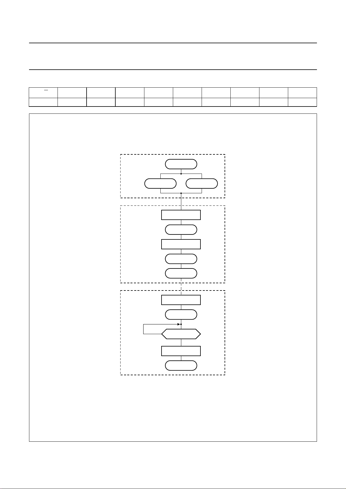
handbook, full pagewidth
Initial state
Booster off
Booster on
Sleep_OUT
send DISPOFF
display off
send BSTROFF
(2)
D31 = 0
booster off
send BSTRON
booster on
display onbooster on
(1)
D31 = 0
(1) When an external V
mode (Partial mode, Scroll mode, etc.) is not affected by sending DISPON/DISPOFF.
(2) D31 is the booster voltage status bit; see Section 6.2.7.
is applied, BSTROFF needs to be sent after reset (default = booster on). The setting of Display
LCD
wait for D31 bit
D31 = 1
send DISPON
display on
MGU916
Fig.7 Recommendation for using commands BSTRON/BSTROFF in combination with DISPON/DISPOFF.
2003 Feb 14 26
Philips Semiconductors Objective specification
STN RGB - 132 × 132 × 3 driver PCF8833
6.2.19 COLUMN ADDRESS SET The display data RAM parameters xs and xe define the column address range of the display data RAM for writing data.
Parameters xs and xe are defined between 0 and 131 (83H), and xs must be smaller then xe.
Table 29 Column address set register bits
D/C76543210DEFAULT
0001010102AH
1 xs[7] xs[6] xs[5] xs[4] xs[3] xs[3] xs[3] xs[0] 02H
1 xe[7] xe[6] xe[5] xe[4] xe[3] xe[2] xe[1] xe[0] 81H
6.2.20 P
The display data RAM parameters ys[7:0] and ye[7:0] define the page (row) address range of the display data RAM for
writing data. Parameters ys and ye are defined between 0 and 131 (83H), and ys must be smaller then ye.
Table 30 Page address set register bits
6.2.21 M
Data written tothe displaymemory (RAM)is validatedby theMemory write(RAMWR) command.Entering thiscommand
always returns the page address and columnaddress to the start addresses xs[7:0] and ys[7:0] respectively.Content of
the display data RAM is written by the data entered following this command, with the page and/or column address
automatically incremented.The data Writemode turned onby this commandcan be automaticallycancelled by entering
another command.
After a power-up the display RAM contentis undefined. Neither a hardwarereset nor a softwarereset changes the data
stored in display RAM. Sending display data must stop 160 ns before issuing a hardware reset, otherwise the last word
written to the display RAM may be corrupted.
Table 31 Memory write register bits
AGE ADDRESS SET
D/
C76543210DEFAULT
0001110112BH
1 ys[7] ys[6] ys[5] ys[4] ys[3] ys[3] ys[3] ys[0] 02H
1 ye[7] ye[6] ye[5] ye[4] ye[3] ye[2] ye[1] ye[0] 81H
EMORY WRITE
D/
C76543210DEFAULT
0001011012CH
1 D7D6D5D4D3D2D1D0XX
2003 Feb 14 27

Philips Semiconductors Objective specification
STN RGB - 132 × 132 × 3 driver PCF8833
6.2.22 COLOUR SET With the Colour set (RGBSET) command the mapping from the 256-colour interface data is translated to the 4 kbyte
colour RAM dataof the PCF8833 can be changed. The translation tablemust be changed, if necessary,before sending
256 colour data. For the red and green pixel 8 from the available 16 grey scales can be selected. For the blue pixel 4
from the 16 grey scales can be selected. The default or reset state of the colour mapping can be found in Table 32.
If the 256-to-4 kbyte colourmapping needsto bechanged, the wholetable mustbe sent.The mapping of colours isdone
when writing data into the RAM, through the application of the Look-Up Table (LUT).
Table 32 Colour set register bits
C D7 D6 D5 D4 D3 D2 D1 D0 DEFAULT DESCRIPTION
D/
000101101 2DH
1 X X X X R3 R2 R1 R0 00H red tone 000
1 X X X X R3 R2 R1 R0 02H red tone 001
1 X X X X R3 R2 R1 R0 04H red tone 010
1 X X X X R3 R2 R1 R0 06H red tone 011
1 X X X X R3 R2 R1 R0 09H red tone 100
1 X X X X R3 R2 R1 R0 0BH red tone 101
1 X X X X R3 R2 R1 R0 0DH red tone 110
1 X X X X R3 R2 R1 R0 0FH red tone 111
1 X X X X G3 G2 G1 G0 00H green tone 000
1 X X X X G3 G2 G1 G0 02H green tone 001
1 X X X X G3 G2 G1 G0 04H green tone 010
1 X X X X G3 G2 G1 G0 06H green tone 011
1 X X X X G3 G2 G1 G0 09H green tone 100
1 X X X X G3 G2 G1 G0 0BH green tone 101
1 X X X X G3 G2 G1 G0 0DH green tone 110
1 X X X X G3 G2 G1 G0 0FH green tone 111
1 X X X X B3 B2 B1 B0 00H blue tone 00
1 X X X X B3 B2 B1 B0 04H blue tone 01
1 X X X X B3 B2 B1 B0 0BH blue tone 10
1 X X X X B3 B2 B1 B0 0FH blue tone 11
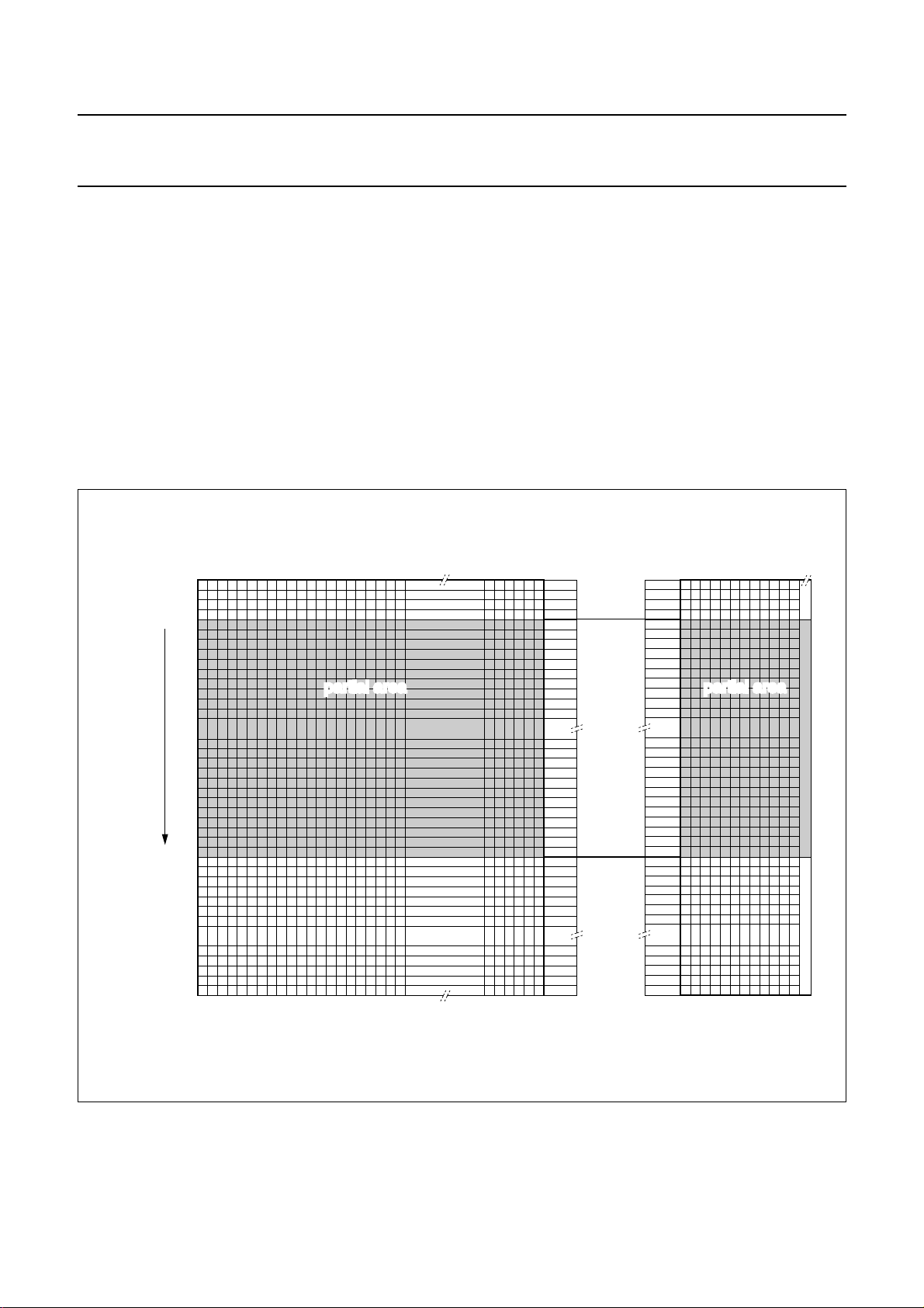
6.2.23 P
ARTIAL AREA
The Partialarea command (PTLAR) sets thepartial display areaand displaysthe RAM contentof this area.In thepartial
Display mode the drive voltage can be reduced.
Table 33 Partial area register bits
D/
C76543210DEFAULT
00011000030H
1 AA1S
1 AA1E
AA1S
7
AA1E
7
AA1S
6
AA1E
6
AA1S
5
AA1E
5
AA1S
4
AA1E
4
AA1S
3
AA1E
3
AA1S
2
AA1E
2
AA1S
1
1
AA1E
0
0
tbf
tbf
2003 Feb 14 28
Philips Semiconductors Objective specification
STN RGB - 132 × 132 × 3 driver PCF8833
The following steps must be followed to enter the Partial
mode:
• Set VOP (when the MMOTP cells are used the VOP for
the Partial mode is predefined)
• Set bias system (when the MMOTP cells are used the
bias system for the Partial mode is predefined)
• Set start address ofactive areaAA1S[7:0]; canbe set in
multiples of 4
• Set end address of active area AA1E[7:0] + 1; can be
set in multiples of 4
• Enter Partial mode (PTLON).
handbook, full pagewidth
AA1S[7:0] = 4
32
rows
AA1E[7:0] +1 = 36
RAM display
When setting the addresses the following conditionsmust
be ensured:
• (AA1E + 1) − AA1S = 32(only 1 partial display size
setting is possible)
• AA1 ≥ 0 and AA1E ≤ 131.
Figure 8 shows how to use the Partial mode with Line
Address Order (LAO) set to logic 0. Figure 9 gives an
example of Partial mode with LAO set to logic 1, and
Fig.10 shows the position of thepartial areawhen thestart
address of the active area is AA1S ≥ (131 + 1) − 31, i.e.
AA1S ≥ 101 (AA1S must be set in multiples of 4).
Figure 11 shows how the Partial mode can be used.
0
1
2
3
4
5
6
7
8
9
10
11
12
13
24
25
26
27
28
29
30
31
32
33
34
35
36
37
38
39
40
41
42
ROW 0
ROW 1
ROW 2
ROW 3
ROW 4
ROW 5
ROW 6
ROW 7
ROW 8
ROW 9
ROW 10
ROW 11
ROW 12
ROW 13
ROW 24
ROW 25
ROW 26
ROW 27
ROW 28
ROW 29
ROW 30
ROW 31
ROW 32
ROW 33
ROW 34
ROW 35
ROW 36
ROW 37
ROW 38
ROW 39
ROW 40
ROW 41
ROW 42
partial areapartial area
Fig.8 Partial Display mode for LAO = 0.
2003 Feb 14 29
127
128
129
130
131
ROW 127
ROW 128
ROW 129
ROW 130
ROW 131
MGU917

Philips Semiconductors Objective specification
STN RGB - 132 × 132 × 3 driver PCF8833
handbook, full pagewidth
AA1E[7:0] +1 = 128
32
rows
AA1S[7:0] = 96
RAM display
0
1
2
3
4
5
6
7
8
9
10
11
12
13
24
25
26
27
28
29
30
31
32
33
34
35
36
37
38
39
40
41
42
127
128
129
130
131
ROW 0
ROW 1
ROW 2
ROW 3
ROW 4
ROW 5
ROW 6
ROW 7
ROW 8
ROW 9
ROW 10
ROW 11
ROW 12
ROW 13
ROW 24
ROW 25
ROW 26
ROW 27
ROW 28
ROW 29
ROW 30
ROW 31
ROW 32
ROW 33
ROW 34
ROW 35
ROW 36
ROW 37
ROW 38
ROW 39
ROW 40
ROW 41
ROW 42
ROW 127
ROW 128
ROW 129
ROW 130
ROW 131
partial areapartial area
MGU918
Fig.9 Partial Display mode for LAO = 1.
2003 Feb 14 30

Philips Semiconductors Objective specification
STN RGB - 132 × 132 × 3 driver PCF8833
handbook, full pagewidth
AA1E[7:0] +1 = 28
AA1S[7:0] = 128
32
rows
RAM display
0
1
2
3
4
5
27
28
29
30
31
32
33
34
35
36
37
38
39
40
41
42
43
44
45
46
47
48
49
50
51
52
53
127
128
129
130
131
ROW 0
ROW 1
ROW 2
ROW 3
ROW 4
ROW 5
ROW 27
ROW 28
ROW 29
ROW 30
ROW 31
ROW 32
ROW 33
ROW 34
ROW 35
ROW 36
ROW 37
ROW 38
ROW 39
ROW 40
ROW 41
ROW 42
ROW 43
ROW 44
ROW 45
ROW 46
ROW 47
ROW 48
ROW 49
ROW 50
ROW 51
ROW 52
ROW 53
ROW 127
ROW 128
ROW 129
ROW 130
ROW 131
partial areapartial area
MGU919
Fig.10 Partial Display mode for LAO = 0 and AA1S[7:0] = 128.
2003 Feb 14 31

Philips Semiconductors Objective specification
STN RGB - 132 × 132 × 3 driver PCF8833
handbook, full pagewidth
Initial state
optional
exit partial mode
(1)
send PTLAR
partial area def
send PTLON
partial mode on
send PTLAR
partial area def
Sleep_OUT
display on normal displaybooster on
send DISPOFF
display off
wait until
display supply
voltage is settled
send DISPON
display on
optional
MGU920
send NORON send SEP
normal display scroll mode
(1) If the initial state is Sleep_IN, the same sequence is valid, but Sleep_OUT has to be sent to see the effect on the display (after the display
voltage has settled).
When sending DAL after PTLON, only thepixels of partial area aredriven on. When sending INVON,in Partialmode only thepixels ofpartial area
are inverted. INVON is over-ruled by DAL and DALO. Pixels outside partial area always stay off.
Fig.11 Recommended sequence for setting Partial mode.
2003 Feb 14 32

Philips Semiconductors Objective specification
STN RGB - 132 × 132 × 3 driver PCF8833
6.2.24 VERTICAL SCROLLING DEFINITION In thePCF8833 three differentscrolling modes can be used.These scrolling modesdiffer from eachother in theway the
RAM to display mapping is done. The vertical scrolling is defined as follows:
• Vertical scrolling definition (VSCRDEF) command
• TF[7:0] defines the number of lines for the top fixed area on the display, there is no top fixed area when TF[7:0] = 0
• SA[7:0] defines the number of lines for the scrolling area on the display
• BF[7:0] defines the number of lines for the bottom fixed area on the display, there is no bottom fixed area when
BF[7:0] = 0.
Figure 12 illustrates the 4 scrolling configurations that can be defined.
Table 34 Vertical scrolling definition register bits
D/C76543210DEFAULT
00011001133H
1TF
1SA
1BF
7TF6
7SA6
7BF6
TF
SA
BF
5
5
5
TF
SA
BF
4
4
4
TF
SA
BF
3
3
3
TF
SA
BF
2
2
2
TF
SA
BF
1
1
1
TF
SA
BF
0
0
0
00H
82H
00H
handbook, full pagewidth
centre screen scroll bottom screen scroll top screen scroll whole screen scroll
Fixed area (RAM content displayed)
Scrolling area
Fig.12 Scrolling modes on the display.
There are 3 different scrolling modes, which are selected as follows:
1. TF + SA + BF = 130 rolling Scroll mode; see Section 6.2.24.1
2. TF + SA + BF = 131 non-rolling Scroll mode; see Section 6.2.24.2
3. TF + SA + BF = 132 non-rolling Scroll mode; see Section 6.2.24.3.
The recommended sequence for setting up the scroll modes is illustrated in Fig.13.
MGU921
2003 Feb 14 33

Philips Semiconductors Objective specification
STN RGB - 132 × 132 × 3 driver PCF8833
handbook, full pagewidth
Initial state
set a new scroll area
(1)
Sleep_OUT
display on
send VSCRDEF
scroll area def
send SEP
scroll mode on
send NORON
normal display
send VSCRDEF
scroll area def
normal displaybooster on
send SEP
scroll mode on
exit scroll mode
send NORON
normal display partial mode
(1) If theinitial state isSleep_IN, the same sequence isvalid, but Sleep_OUThas to besent to see the effect on the display(after the
display voltage has settled).
send PLTON
MGU922
Fig.13 Recommended sequence for setting up Scroll modes.
2003 Feb 14 34

Philips Semiconductors Objective specification
STN RGB - 132 × 132 × 3 driver PCF8833
6.2.24.1 Rolling Scroll mode
The RAM-to-display mapping for the rolling Scroll mode
when a 132 × 130 (columns × rows) display is connected
to the PCF8833 is illustrated in Fig.14. In this case rows
0 and 131 must beleft open. When a132 × 132 display is
connected, there will be a one-to-one mapping between
the RAM and the display, and there will be no unused
rows.
The rolling Scroll mode is activated when the Set Entry
Scroll Point (SEP) is set; see Table 35.
Figure 15 gives an example for when the PCF8833 is
working in the rolling Scroll mode.
When the rolling Scroll mode is used the following
sequence can be applied:
• After the desired time interval increment the scroll
address to SEP + n for a n-line step
• Keep incrementing the scroll address (SEP) at regular
intervals.
The rolling Scroll mode is left when the normal Display
mode on (NORON) or the partial Display mode on
(PTLON) is selected.
Table 35 Set entry scroll point register bits
D/C7D6543210DEFAULT
00011011137H
1 SEP7 SEP6 SEP5 SEP4 SEP3 SEP2 SEP1 SEP0 00H
handbook, full pagewidth
]
TF[7:0
RAM (132 x 132)
display (132 x 130)
0
1
2
3
4
5
6
7
8
0
0
1
2
3
4
5
6
7
8
TF[7:0
]
]
SA[7:0
121
2 unused
rows
BF[7:0
]
122
123
124
125
126
127
128
129
130
131
Fig.14 RAM to display mapping for the rolling Scroll mode (TF + SA + BF = 130) for LAO = 0.
2003 Feb 14 35
120
121
124
125
126
127
128
129
130
131
131
MGU923
SA[7:0
BF[7:0
]
]

Philips Semiconductors Objective specification
STN RGB - 132 × 132 × 3 driver PCF8833
handbook, full pagewidth
TF = 8
2 unused
rows
BF = 8
RAM (132 x 132) display (132 x 130)
0
1
2
3
4
5
6
7
8
]
SEP[7:0
121
122
123
124
125
126
127
128
129
130
131
SEP
120
121
SEP−1
124
125
126
127
128
129
130
131
131
MGU924
0
0
1
2
3
TF = 8
4
5
6
7
SA = 114
8
9
BF = 8
Fig.15 The rolling Scroll mode (TF + SA + BF = 130) for LAO = 0.
2003 Feb 14 36

Philips Semiconductors Objective specification
STN RGB - 132 × 132 × 3 driver PCF8833
6.2.24.2 Non-rolling Scroll mode
The RAM-to-display mapping for the non-rolling Scroll
mode when a 132 × 130 (columns × rows) display is
connected to the PCF8833 is illustrated in Fig.16. In this
case unused rows and columns are to be left open, for
instance row 0 and 131. If a 132 × 132 display is
connected to the PCF8833 the content of row 0 and 131
will bethe sameas the contentwhich isdisplayed in row 1
and 130, respectively. By doing so, the display data RAM
will have 1 row in the background, whose content can be
updated when it is not displayed.
The non-rolling Scroll mode is activated when the Set
Entry Scroll point is set; see Table Fig.36.
An example is given in Figure 17 for the case when the
PCF8833 is working in the non-rolling Scroll mode
(TF + SA + BF = 131).
When the non-rolling Scroll mode is used the following
sequence can be applied:
• Fill the background memory
• After the desired time interval increment the scroll
address to SEP + n for a n-line step
• Keep filling the background memory and incrementing
scroll address (SEP) at regular intervals to obtain a
smooth scrolling.
Thenon-rolling Scrollmodeis leftwhenthe normalDisplay
mode on (NORON) or the partial Display mode on
(PTLON) is selected.
Table 36 Set entry scroll point register bits
D/C76543210DEFAULT
00011011137H
1 SEP7 SEP6 SEP5 SEP4 SEP3 SEP2 SEP1 SEP0 00H
handbook, full pagewidth
]
TF[7:0
]
SA[7:0
1 buffer
row
1 unused
row
]
BF[7:0
RAM (132 x 132)
display (132 x 130)
120
121
124
125
126
127
128
129
130
131
131
MGU925
0
0
1
2
3
4
5
6
7
8
TF[7:0
SA[7:0
BF[7:0
]
] −
1
]
0
1
2
3
4
5
6
7
8
121
122
123
124
125
126
127
128
129
130
131
Fig.16 RAM to display mapping for the non-rolling Scroll mode (TF + SA + BF = 131) for LAO = 0.
2003 Feb 14 37

Philips Semiconductors Objective specification
STN RGB - 132 × 132 × 3 driver PCF8833
handbook, full pagewidth
TF = 8
1 buffer row
1 unused row
BF = 8
RAM (132 x 132) display (132 x 130)
0
1
2
3
4
5
6
7
8
]
SEP[7:0
121
122
123
124
125
126
127
128
129
130
131
SEP
121
122
SEP−2
124
125
126
127
128
129
130
131
131
MGU926
0
0
1
2
3
4
5
6
7
8
9
TF = 8
SA − 1 = 114
BF = 8
Fig.17 The non-rolling Scroll mode (TF + SA + BF = 131) for LAO = 0.
6.2.24.3 Non-rolling Scroll mode
The RAM-to-display mapping for the non-rolling Scroll
mode when a 132 × 130 (columns × rows) display is
connected to the PCF8833 is illustrated in Fig.18. In this
case unused rows and columns are to be left open, for
instance row 0 and 131. If a 132 × 132 display is
connected to the PCF8833 the content of row 0 and 131
will be the same as the content which is displayed in row
1 and 130,respectively. Bydoing sothe displaydata RAM
will have2 rows in the background,whose content can be
updated when they are not displayed.
The non-rolling Scroll mode is activated when the Set
Entry Scroll Point is set; see Table Fig.37.
Figure 19 shows an example for when the PCF8833 is
working in the non-rolling Scroll mode
(TF + SA + BF = 132).
When the non-rolling Scroll mode is used the following
sequence can be applied.
• Fill the background memory
• After the desired time interval increment the scroll
address to SEP + n for a n-line step
• Keep filling the background memory and incrementing
scroll address (SEP) at regular intervals to obtain a
smooth scrolling.
Thenon-rolling Scrollmodeis leftwhenthe normalDisplay
mode on (NORON) or the partial Display mode on
(PTLON) is selected.
2003 Feb 14 38

Philips Semiconductors Objective specification
STN RGB - 132 × 132 × 3 driver PCF8833
Table 37 Set entry scroll point register bits
D/C76543210DEFAULT
00011011137H
1 SEP7 SEP6 SEP5 SEP4 SEP3 SEP2 SEP1 SEP0 00H
handbook, full pagewidth
]
TF[7:0
]
SA[7:0
2 buffer
rows
]
BF[7:0
RAM (132 x 132)
display (132 x 130)
120
121
124
125
126
127
128
129
130
131
131
MGU927
0
0
1
2
3
4
5
6
7
8
TF[7:0
SA[7:0
BF[7:0
]
] −
2
]
0
1
2
3
4
5
6
7
8
121
122
123
124
125
126
127
128
129
130
131
Fig.18 RAM to display mapping for the non-rolling Scroll mode (TF + SA + BF = 132) for LAO = 0.
2003 Feb 14 39

Philips Semiconductors Objective specification
STN RGB - 132 × 132 × 3 driver PCF8833
handbook, full pagewidth
TF = 8
2 buffer rows
BF = 8
RAM (132 x 132) display (132 x 130)
0
1
2
3
4
5
6
7
8
]
SEP[7:0
121
122
123
124
125
126
127
128
129
130
131
SEP
122
123
SEP−3
124
125
126
127
128
129
130
131
131
MGU928
0
0
1
2
3
4
5
6
7
8
9
TF = 8
SA − 2 = 114
BF = 8
Fig.19 The non-rolling Scroll mode (TF + SA + BF = 132) for LAO = 0.
2003 Feb 14 40

Philips Semiconductors Objective specification
STN RGB - 132 × 132 × 3 driver PCF8833
6.2.24.4 Effect of LAO on scroll modes
An exampleof when the PCF8833is working inthe non-rolling Scroll mode(TF + SA + BF = 132) with the Line Address
Order (LAO) bit set to logic 1, is illustrated in Fig.20. The Scroll modes described in Sections 6.2.24.1and 6.2.24.2 also
work on the same principle when the LAO bit is set to logic 1.
handbook, full pagewidth
BF = 8
2 buffer rows
TF = 8
RAM (132 x 132) display (132 x 130)
0
1
2
3
4
5
6
7
8
9
10
]
SEP[7:0
123
124
125
126
127
128
129
130
131
SEP+3
123
SEP−1
SEP
124
125
126
127
128
129
130
131
131
MGU929
0
0
1
2
3
4
5
6
7
8
9
BF = 8
SA − 2 = 114
TF = 8
Fig.20 The non-rolling Scroll mode (TF + SA + BF = 132); with LAO = 1.
2003 Feb 14 41

Philips Semiconductors Objective specification
STN RGB - 132 × 132 × 3 driver PCF8833
6.2.25 TEARING EFFECT LINE OFF The Tearing effect line off (TEOFF) command ties the TE pin LOW.
Table 38 Tearing effect line off register bits
D/
C76543210DEFAULT
00011010034H
6.2.26 T
EARING EFFECT LINE ON
The Tearing effect line on (TEON) command turns the TE line of the display on.
The TE signal indicates the start of a super-frame (equals 16 frames). In 4 kbyte colour mode a whole super-frame is
needed to write full colour depth. In 8-colour mode the available colour depth is written in one frame.The tearing signal
goes HIGH when the last line of a super-frame is read. The HIGH time is 850 µs (see Fig.21).
Table 39 Tearing effect line on register bits; note 1
C76543210DEFAULT
D/
00011010135H
1XXXXXXXX00H
Note
1. X = don’t care.
handbook, full pagewidth
TE signal
superframe period
(16 frames )
850 µs
Fig.21 Tearing effect line: distribution of pulses.
2003 Feb 14 42
MGU930

Philips Semiconductors Objective specification
STN RGB - 132 × 132 × 3 driver PCF8833
6.2.27 MEMORY DATA ACCESS CONTROL The displaydata RAM access conditions canbe defined byusing the Memorydata access control(MADCTL) command. The used single control bits together with their reset states are given in Table 41.
Table 40 Memory data access control register bits
D/C76543210DEFAULT
00011011036H
1 MY MX V LAO
(1)
Note
1. Refer toSection 6.2.24.4 for anexplanation of LAOon scroll modesand to Section 6.2.23for an explanationof LAO
on Partial mode.
Table 41 Explanation of the memory data access control bits
BIT LOGIC 0 (RESET STATE) LOGIC 1
MY no mirror Y mirror Y
MX no mirror X mirror X
V RAM write in X direction vertical RAM write; in Y direction
LAO line address order (top to bottom) line address order (bottom to top)
RGB RGB BGR
RGB X X X 00H
The relationship between RAM and display for the MX, MY, RGB and LAO control bits is illustrated Fig.22.
Combinations of MX, MY and V are described in more detail in Section 7.2.
handbook, full pagewidth
page address
interface
131
column drivers
D3 = 0:RGB
131
2
1
0
D6 = 0
D6 = 1
D3 = 1:BGR
0,0
012
column address
0
1
2
RAM
131
131
012131
MGU931
D7 = 1D7 = 0
0
1
2
D4 = 1D4 = 0
131
2
1
0
DISPLAY
row drivers
Fig.22 Display data RAM access control.
2003 Feb 14 43

Philips Semiconductors Objective specification
STN RGB - 132 × 132 × 3 driver PCF8833
6.2.28 IDLE MODE OFF
The Idle mode off(IDMOFF) command turns off the Idle mode and the PCF8833 is working in the 4 kbyte colour mode.
This command is similar to the Idle mode on command (IDMON); see Section 6.2.29.
Table 42 Idle mode off register bits
D/C76543210DEFAULT
00011100038H
6.2.29 I
The Idle mode on (IDMON) command activates the Idle mode of the LCD driver in order to reduce the power
consumption. When theIdle mode is switched on,the number of colours isreduced to 8 (only the MSBof data stored in
the RAM is used). In addition to the reduction in the number of colours, the frame frequency can also be reduced. The
frame frequencyfor the Idlemode can be programmed separately from the framefrequency in 4 kbytecolour mode; see
Section 6.2.41.
Table 43 Idle mode on register bits
6.2.30 C
By using the Colour interface pixel format command (COLMOD) different interface RGB formats can be chosen. The
choice of an RGB format also influences the way display data is transferred to the display data RAM via the interface;
see Section 7.1.3.
The different interface RGB formats are given in Table 45.
Table 44 Colour interface pixel format register bits; note 1
DLE MODE ON
C76543210DEFAULT
D/
00011100139H
OLOUR INTERFACE PIXEL FORMAT
C76543210DEFAULT
D/
0001110103AH
1XXXXXP2P1P003H
Note
1. X = don’t care.
2003 Feb 14 44

Philips Semiconductors Objective specification
STN RGB - 132 × 132 × 3 driver PCF8833
Table 45 Interface formats
P2 P1 P0
INTERFACE
FORMATS
0 0 0 no action
0 0 1 no action
0 1 0 8-bit/pixel
0 1 1 12-bit/pixel
(1)
(2)
1 0 0 no action
1 0 1 16-bit/pixel
(3)
1 1 0 no action
1 1 1 no action
Notes
1. PCF8833 is switched into 256 colour mode,
256 colours are mapped to the 4 kbyte RAM with a
LUT; see Section 6.2.22.
2. PCF8833 is switchedinto 4 kbyte colour mode, which
is also the reset state.
3. PCF8833is switched into64 kbytecolour mode, which
is achieved by means of dithering.
6.2.31 SET V
OP
The set VOPcommand (SETVOP) is used to program the
optimum LCD supply voltage V
LCD
.
The reset state of VPR[8:0] is 257DEC (13.88 V).
The optimum LCD supply voltage can be calculated as
explainedin Section 6.2.43.TheVOPvalueis programmed
via the VPR register. Besides the VPR register the V
OP
value can be calibrated by meansof OTPcells orchanged
with the VCON register (see Fig.23).
The generated V
can be calculated with equation (1).
LCD
Figure 24 is the graphical equivalent to equation (1).
V
V
a MMVOPCAL 5:0[]VCON 6:0[]
LCD
PR
+=
8:0[]
〉b×
++〈
(1)
Where:
• a is a fixed constant value; see Table 47
• b is a fixed constant value; see Table 47
• VPR[8:0] is the programmed VOP value; the
programming range for VPR[8:0] is 5 to 410 (19AH)
• MMVOPCAL[5:0] is the value of the offset stored in the
OTP cells in twos complement format; see Section 15.1
• VCON[6:0] is the setcontrast valuewhich canbe setvia
the interface and is in twos complement format; see
Section 6.2.16.
The VOP[8:0] value must be in the V
programming
LCD
range as shown in Fig.24. Evaluating equation (1),values
outside ofthe programming range indicated in Fig.24 may
result. Calculated values below 0 will be mapped to
VOP= 0; resulting VOP values higher than 445 will be
mapped to VOP= 445. An overview of the complete
programming range of V
can be found in Section 15.1.
LCD
As the programming range for the internally generated
V
allows values above the maximum allowed V
LCD
(20 V) the user has to ensure, while setting the V
LCD
PR
register andselecting thetemperature compensation, that
under all conditions and including all tolerances the V
LCD
remains below 20 V.
Table 46 Set V
CD7D6D5D4D3D2D1D0DEFAULT
D/
register bits; note 1
OP
010110000B0H
1XXXXVPR
1XXXVPR
4
VPR
8
3
VPR
VPR
7
2
VPR
VPR
6
1
VPR
VPR
5
0
08H
01H
Note
1. X = don’t care.
2003 Feb 14 45

Philips Semiconductors Objective specification
STN RGB - 132 × 132 × 3 driver PCF8833
Table 47 Parameters of V
SYMBOL VALUE UNIT
b 0.04 V
a 3.6 V
handbook, full pagewidth
8 7 6 5 4 3 2 1 0
LCD
[
]
8:0
V
PR
VCON[6:0
]
MMVOPCAL[5:0
]
[
]
8:0
V
OP
ab
V
LCD
MGU932
Fig.23 Setting of VOP.
handbook, full pagewidth
V
LCD
a
00 01 02
03 04 05
b
06
Fig.24 V
programming range (05H to 19AH)
. . .
programming range of the PCF8833.
LCD
410DEC
MGU933
V
OP
2003 Feb 14 46

Philips Semiconductors Objective specification
STN RGB - 132 × 132 × 3 driver PCF8833
6.2.32 BOTTOM ROW SWAP The Bottom Row Swap(BRS) command enables the bottom rows of the PCF8833 to be swapped (mirrored) in order to
make an optimum glass layout.
The function of the BRS command in combination with the function of the Top Row Swap (TRS) is illustrated in
Figures 25, 26, 27 and 28. A description of the TRS function is given in Section 6.2.33.
The reset state of the BRS command is defined in Table 49.
Table 48 Bottom row swap register bits
D/C76543210DEFAULT
01011010BRSB4H
Table 49 Bottom row swap reset state
BIT LOGIC 0 (RESET STATE) LOGIC 1
BRS bottom rows are not mirrored bottom rows are mirrored
6.2.33 TOP ROW SWAP The Top Row Swap (TRS) command enables the top rows of the PCF8833 to be swapped (mirrored) in order to make
an optimum glass layout.
The function of the TRS command in combination with BRS is illustrated in Figures 25, 26, 27 and 28. The description
of BRS function can be found in Section 6.2.32.
The reset state of the TRS command is given in Table 51.
Table 50 Top row swap register bits
CD7D6D5D4D3D2D1D0DEFAULT
D/
01011011TRSB6H
Table 51 Top row swap reset state
BIT LOGIC 0 (RESET STATE) LOGIC 1
TRS top rows are not mirrored top rows are mirrored
2003 Feb 14 47

Philips Semiconductors Objective specification
STN RGB - 132 × 132 × 3 driver PCF8833
handbook, full pagewidth
36 rows 32 rows
32 rows 32 rows
64
95
96
131
96131
PCF8833
6495
columns
DISPLAY
6332
310
31
32
63
MGU934
0
Fig.25 Row sequence for BRS = 0 and TRS = 0.
handbook, full pagewidth
36 rows 32 rows
32 rows 32 rows
64
95
96
131
13196
PCF8833
6495
columns
DISPLAY
Fig.26 Row sequence for BRS = 0 and TRS = 1.
2003 Feb 14 48
3263
310
31
32
63
MGU935
0

Philips Semiconductors Objective specification
STN RGB - 132 × 132 × 3 driver PCF8833
handbook, full pagewidth
36 rows 32 rows
64
95
96
131
96131 6332
PCF8833
9564 032
columns
DISPLAY
32 rows32 rows
0
31
32
63
MGU936
Fig.27 Row sequence for BRS = 1 and TRS = 0.
handbook, full pagewidth
36 rows 32 rows
64
95
96
131
13196
PCF8833
9564
columns
DISPLAY
Fig.28 Row sequence for BRS = 1 and TRS = 1.
2003 Feb 14 49
3263
031
32 rows32 rows
0
31
32
63
MGU937

Philips Semiconductors Objective specification
STN RGB - 132 × 132 × 3 driver PCF8833
6.2.34 SUPER FRAME INVERSION The Super frame inversion command (FINV), which is the inversion of the row functions after all rows are written to can
be switchedoff for the PCF8833.When switched off, the inversion of therow functions will then only be donewith N-line
inversion. Inversion of the row functions is needed so as to avoid a DC component over the LCD display. A detailed
description of the N-line inversion is given in Section 6.2.45.
The FINV control bit reset state is defined in Table 52.
Table 52 Super frame inversion register bits
D/C76543210DEFAULT
0 1 0 1 1 1 0 0 FINV B9H
Table 53 Super frame inversion reset state
BIT LOGIC 0 LOGIC 1 (RESET STATE)
FINV super frame inversion is off super frame inversion is on
6.2.35 DATA ORDER The data order (DOR) of the data which will be written into the RAM can be changed (swapped). The DOR command is explained and the reset state defined in Table 55.
Table 54 Data order register bits
D/C76543210DEFAULT
0 1 0 1 1 1 0 1 DOR BAH
Table 55 Data order reset state
BIT LOGIC 0 (RESET STATE) LOGIC 1
DOR normal data order MSB/LSB transposed for RAM data
6.2.36 TEMPERATURE COMPENSATED FRAME FREQUENCY The PCF8833 incorporates a temperature segmented frame frequency programming; see Section 6.2.41. This
segmented frame frequency can be disabled by using the temperature compensated frame frequency (TCDFE)
command.
The TCDFE control bit reset state is defined in Table 57.
When the non-segmented frame frequency is chosen, the frame frequency in segment B (DFB) is valid;
see Section 6.2.41.
Table 56 Temperature compensated frame frequency register bits
D/C76543210DEFAULT
0 1 0 1 1 1 1 0 TCDFE BDH
2003 Feb 14 50

Philips Semiconductors Objective specification
STN RGB - 132 × 132 × 3 driver PCF8833
Table 57 Temperature compensated frame frequency reset state
BIT LOGIC 0 LOGIC 1 (RESET STATE)
TCDFE non-segmented frame frequency segmented frame frequency
6.2.37 T
EMPERATURE COMPENSATED V
LCD
The PCF8833 incorporates a temperaturesegmented VOPprogramming; see Section 6.2.40. By usingthe temperature
compensated V
(TCVOPE) command the temperature segmented V
LCD
can be disabled.
LCD
The TCVOPE control bit reset state is defined in Table 59.
When the non-segmented V
programming is chosen the LCD supply voltage is flat, i.e. no compensation over the
LCD
specified temperature range (offset VT in Fig.30 is 0).
The TCVOPE command is also used to read back the temperature via the interface; see Section 6.2.44.
Table 58 Temperature segmented V
C76543210DEFAULT
D/
register bits
LCD
0 1 0 1 1 1 1 1 TCVOPE BFH
Table 59 Temperature segmented V
reset state
LCD
BIT LOGIC 0 LOGIC 1 (RESET STATE)
TCVOPE no temperature compensated V
6.2.38 I
NTERNAL OR EXTERNAL OSCILLATOR
LCD
segmented temperature compensated V
LCD
The Internal/external oscillator (EC) command selects the internal or external oscillator. When an external oscillator is
used the external clock signal has to be connected to the OSC pad; see Section 7.6.
The EC control bit reset state is defined in Table 61.
Table 60 Internal/external oscillator register bits
D/C76543210DEFAULT
01100000ECC0H
Table 61 Internal/external oscillator reset state
BIT LOGIC 0 (RESET STATE) LOGIC 1
EC internal oscillator external clock applied
2003 Feb 14 51

Philips Semiconductors Objective specification
STN RGB - 132 × 132 × 3 driver PCF8833
6.2.39 SET MULTIPLICATION FACTOR The Set multiplication factor (SETMUL) command sets the multiplication factor of voltage multiplier 1. A detailed
explanation of the LCD voltage supply architecture is given in Section 7.8.
The different multiplication factor settings for voltage multiplier 1 are given in Table 63.
Table 62 Set multiplication factor register bits; note 1
D/CD7D6D5D4D3D2D1D0DEFAULT
011000010C2H
1XXXXXXS1S003H
Note
1. X = don’t care.
Table 63 Multiplication factor settings voltage multiplier
S1 S0 MULTIPLICATION FACTOR
002×multiplication
013×multiplication
104×multiplication
115×multiplication; note 1
Note
1. Reset state.
6.2.40 SET TCVOP SLOPES A, B, C AND D The Set TCVOP slopes A, B, C and D (TCVOPAB and TCVOPCD) command splits the temperature range into 4 parts
and can be programmed by using the following commands.
Due to the temperature dependency of the liquid crystals viscosity, the LCD controlling voltage V
might have to be
LCD
adjusted at different temperatures to maintain optimum contrast.
There arefour equally spaced temperatureregions. For each temperature region a differenttemperature coefficient can
be selected. Each coefficient can be selected from a choice of eight different slopes, or multiplication factors
(see Table 66)by settingTCVOPAB andTCVOPCD.The controlledV
willnot bechanged linearly, butin 40 mVsteps
LCD
(parameter b in Table 47). Slopes SLA, SLB, SLC and SLD are overwritten by OTP values if these are set.
Table 64 Set TCVOP slopes A and B register bits; note 1
D/
C76543210DEFAULT
011000011C3H
1 X SLB
2
SLB
1
SLB
0
X SLA
2
SLA
1
SLA
0
34H
Note
1. X = don’t care.
2003 Feb 14 52

Philips Semiconductors Objective specification
STN RGB - 132 × 132 × 3 driver PCF8833
Table 65 Set TCVOP slopes C and D register bits; note 1
D/C76543210DEFAULT
011000100C4H
1 X SLD
2
Note
1. X = don’t care.
Table 66 Set TCVOP slopes multiplication factors; note 1
SLD
1
SLD
0
X SLC
2
SLC
1
SLC
0
75H
SLA[2:0]
SLB[2:0]
SLC[2:0]
SLD[2:0]
MA
MB
MC
MD
111 1.250 −53.33 mV/°C
110 1.000 −42.66 mV/°C
101 0.875 −37.33 mV/°C
100 0.750 −32.00 mV/°C
011 0.625 −26.66 mV/°C
010 0.500 −21.33 mV/°C
001 0.375 −16.00 mV/°C
000 0.250 −10.66 mV/°C
Note
1. For the reset state refer to Table 4. Values overwritten by OTP.
handbook, full pagewidth
V
LCD
MA MCMB MD
SLOPE
MGU938
20 50 80−40 −10
Fig.29 Example of segmented temperature coefficients.
2003 Feb 14 53
T (°C)

Philips Semiconductors Objective specification
STN RGB - 132 × 132 × 3 driver PCF8833
Temperature compensation is implemented by adding an
offset to the VOPvalue. Previously, in Section 6.2.31, V
OP
was calculated by adding VPR, VCON and MMVOPCAL
settings together. Now, an additional offset VTis added.
The final result for V
calculation is a 9-bit positive
LCD
number. Care must betaken bythe userto ensurethat the
ranges of VPR, MMVOPCAL, VCON and temperature
compensationdo notcause clipping,and henceundesired
results (seeFig.24). Theadders will notpermit overflowor
underflow and will clamp results to eitherend of the range
(VOP= 0 or 445). Also, temperatures outside the range
−40 to +79 °C will be clamped to the last valid offset.
Thetemperature readoutgenerates an8-bitresult TD[7:0].
This temperature readout number is used fortemperature
compensation.
handbook, full pagewidth
SLB SLC SLD
SLA
The resolution of the readout is
(−40 to +80 °C)/128 = 0.9375 °C/LSB; where 0
represents −40 °C and 127 represents +79 °C;
see Section 6.2.44.
Thetemperature readoutfunctioncan alsobeused toread
back the temperature value via the interface;
see equation (12).
The offset value may be calculated from Table 67. The
effect on V
can be calculated by multiplying the offset
LCD
value with the value of b.
For example T = −8 °C: TD = 34 and MB = 0.5:
V
LCD(OS)
A complete overview of the programming range of V
=40mV×(64 − 34) × 0.5 = 600 mV.
LCD
can be found in Section 15.1.
TEMPERATURE
READOUT
8TD
−40
zero
offset
VCON[5:0
[
]
8:0
+80
T (°C)
]
0
V
PR
OFFSET
MMVOPCAL[5:0
V
OP
8
V
T
ab
]
[
]
8:0
9
V
MGU939
LCD
Fig.30 Segmented temperature compensation.
2003 Feb 14 54

Philips Semiconductors Objective specification
STN RGB - 132 × 132 × 3 driver PCF8833
Table 67 Offset value
TEMPERATURE RANGE TD EQUIVALENT OFFSET EQUATION VT
<−40 °C032×(MB + MA)
−40 °C to < −10 °C 0 to 31 (32 × MB)+MA×(32 − TD)
−10 to < 20 °C 32 to 63 (64 − TD) × MB
20 °Cto<50°C64to95−(TD − 64) × MC
50 to < 80 °C 96 to 127 −((32 × MC) + MD × (TD − 96))
≥80 °C >127 −(32 × MC + 31 × MD)
6.2.41 FRAME FREQUENCY PROGRAMMING The PCF8833 incorporates temperature segmented
Frame frequency programming (TCDF). The temperature
range is split into 4 areas as shown in Fig.31.
In each of the segments a Division Factor (DF) can be
programmed which determines the Frame Frequency
(FF). In equation (2) the frame frequency can be
calculated from a given division factor.
1
×
f
--------- -
osc
132
=
FF
------------------------- DF
Where f
is the oscillator frequency which is defined in
osc
Chapter 13.
The Divider Factor (DF) is a 7-bit number so the upper
programming range is limited to 127DEC resulting in a
minimum frame frequency of 35.8 Hz. The lower
programming range is limited to 20DEC resulting in a
maximum frame frequency of 227 Hz. The frame
frequency is derived from the built-in oscillator, and thus
the tolerance of the frame frequencyhas thesame ratioas
that given for the oscillator frequency; see Chapter 13.
(2)
When Partial mode is selected (see Sections 6.2.10 and
6.2.23) the same segmented frame frequencies will be
used as for the full Display mode.
Table 68 Frame frequency programming register bits; note 1
D/
C76543210DEFAULT
011000101C5H
1 X DFA
1 X DFB
1 X DFC
1 X DFD
6
6
6
6
DFA
DFB
DFC
DFD
5
5
5
5
DFA
DFB
DFC
DFD
4
4
4
4
DFA
DFB
DFC
DFD
3
3
3
3
DFA
DFB
DFC
DFD
2
2
2
2
DFA
DFB
DFC
DFD
1
1
1
1
DFA
DFB
DFC
DFD
0
0
0
0
38H
35H
30H
25H
Note
1. X = don’t care.
2003 Feb 14 55

Philips Semiconductors Objective specification
STN RGB - 132 × 132 × 3 driver PCF8833
handbook, full pagewidth
DFA DFCDFB DFD
frame
frequency
MGU940
35 49 79−40 −11
T (°C)
Fig.31 Segmented temperature frame frequency.
6.2.42 FRAME FREQUENCY PROGRAMMING IN 8-COLOUR MODE
When the Idle mode is selected (see Section 6.2.29) the frame frequency is determined from division factor DF8. In the
Idle mode thePCF8833 works in 8-colour mode and therefore a lower frame frequency can be chosen which willbe the
same over the whole temperature range. Calculation of the frame frequency and determining the division factor is the
same as explained in Section 6.2.41.
When Partial mode is selected (see Sections 6.2.10 and 6.2.23) the same frame frequency will be used as for the full
Display mode in Idle mode.
Table 69 Frame frequency programming in 8-colour mode register bits; note 1
D/
C76543210DEFAULT
011000110C6H
1 X DF8
6
DF8
5
DF8
4
DF8
3
DF8
2
DF8
1
DF8
0
35H
Note
1. X = don’t care.
6.2.43 SET BIAS SYSTEM The LCD supply voltage and the bias voltages, which can be chosen,depend on the Liquid Crystal (LC) that is used.In
equation (3) the relationship between the VON/V
ratio of LC parameters and the bias system (a) for a given display
OFF
size (N) is given.
V
ON
------------V
OFF
2
a
-----------------------------=
a2N2a–+
N2a++
(3)
2003 Feb 14 56

Philips Semiconductors Objective specification
STN RGB - 132 × 132 × 3 driver PCF8833
When the required bias system (a) is defined, the LCD
supply voltage for a display size Ncan bedetermined; see
equation (4).
LCD
2a VON×
-------------------------------------- -×=
Pa
N
2
N2a++()
(4)
The parameter P in equation (4) is the number of
simultaneous selected rows. For the maximum number of
rows of 132, P = 4 is chosen. When partial Display mode
is selected the P value is set to 1 internally.
handbook, full pagewidth
V
LCD2
V2H
V1H
VC
V1L
V2L
V
SS
P = 4
F
G
VC
−G
−F
max
max
The bias voltages needed in a MRA LCD driver depends
on the number of simultaneous selected rows (P). The
bias voltages of the PCF8833 are given for P = 4 and
P = 1; see Fig.32. In the PCF8833 the maximum column
voltage (GMAX) is always lower or equal to the row
voltage F.
V
LCD2
V2H
V2L
V
VC
SS
P = 1
F
G
max
VC
−G
max
−F
MGU941
Fig.32 Bias levels for a MRA system with P = 4 and P = 1.
The bias voltage levels are a function of the row voltage
F and a:
V
=
F
------------ -
FG
≥
max
G
=
F
---------------------- -
F
------------- G
max
LCD
2
max
=
a×
p
a
-- p
(5)
(6)
(7)
(8)
Depending on the value of p, the bias levels are set in the
ratio of:
p=1:αR−2R − 2R −αR
p=4:αR−R−R−R−R−αR
Where the value of α is in the range from 0 to 4.
The value of F is determined by (α +2)×R and the value
of G
The relationship between the ratio F/G
------------- G
is determined by 2 × R.
max
a
F
max
α 2+()R×
-- -
---------------------------- -
p
2R×
α 2+()
----------------- 2
max
1
and α:
α
+== = =
--2
(9)
or:
α
-------------
G
max
1–
2×=
(10)
F
The relationbetween a and α fora given p is the following:
α
a
---
2
1+
p×= α
a
1–
-- -
p
2×=
(11)
This leads tothe following bias systems givenin Table 70.
2003 Feb 14 57

Philips Semiconductors Objective specification
STN RGB - 132 × 132 × 3 driver PCF8833
Table 70 Bias system ratios
VB[3:0] F/G
max
α
P=1(N=32)
(1)
P=4(N=132)
0000 1.000 0.00 not allowed not allowed
0001 1.250 0.50
0010 1.375 0.75
0011 1.500 1.00 1.500
0100 1.625 1.25 1.625
0101 1.750 1.50 1.750
0110 1.875 1.75 1.875
0111 2.000 2.00 2.000 8.0
1000 2.125 2.25 2.125 8.5
1001 2.250 2.50 2.250 9.0
1010 2.375 2.75 2.375 9.5
1011 2.500 3.00 2.500 10.0
1100 2.625 3.25 2.625 not allowed
1101 2.750 3.50 2.750
1110 2.875 3.75 2.875
1111 3.000 4.00 3.000
Notes
1. For Partial mode internally P = 1 is set, otherwise P = 4 is selected. Limitations for Partial mode given in
Section 6.2.43.2 for respectively for full Display mode given in Section 6.2.43.1 have to be taken into account.
2. Reset state.
a
(1)
(2)
Table 71 Set bias system register bits; note 1
C76543210DEFAULT
D/
011000111C7H
1XXXXVB
3VB2
VB
1
VB
0
0BH
Note
1. X = don’t care.
6.2.43.1 Limitations on bias voltages in Normal mode
V
: 1.5 to 3.3 V
DD1
V
: 5.5 to 11 V
LCD1
V
: 10 to 20 V
LCD2
(V
− V
LCD2
V
LCD2
----------------
2
but for V
LCD1
–
V
LVD1
: 10 to 11 V:
LCD2
): 4.5 to 9 V
0 to 1 V=
V
LCD2
----------------
V
–
2
LCD1
0 to 0.5 V=
6.2.43.2 Limitations on bias voltages in Partial mode
V
: 1.5 to 3.3 V
DD1
V
: 2.9 to 12 V
LCD1
V
: 3.8 to 12 V
LCD2
–()
V
LCD2VLCD1
max
0.5 V=
2003 Feb 14 58

Philips Semiconductors Objective specification
STN RGB - 132 × 132 × 3 driver PCF8833
6.2.44 TEMPERATURE READBACK
The PCF8833 has a built-in temperature readback
(RDTEMP) measurement device. The measured value is
provided as an 8-bit digital value TD[7:0] which can be
read back via the interface.
The temperature can be determined from TD[7:0] using
the following formula:
T 0.9375 TD 40–×()°C=
(12)
A measurementcan beinitiated by sendingthe instruction
to setTCVOPE (toeither logic 1 or logic 0),irrespective of
whether temperature compensation is disabled or not.
After initialization, the measurement will take
approximately 5 ms to complete. It is recommended to
read the register twice to qualify the returned result,
especially if the measurement is triggered automatically.
The input and output data format for the temperature
readback is given in Table 73.
Temperature measurements are started automatically
every ten seconds when the digital temperature
compensation is active (default).
Table 72 Temperature readback register bits
D/
C76543210DEFAULT
011011000C8H
Table 73 Temperature readback data format
SYMBOL D/
C76543210DEFAULT
(S)DIN 011011000C8H
(S)DOUT − TD[7] TD[6] TD[5] TD[4] TD[3] TD[2] TD[1] TD[0] XX
6.2.45 N-
LINE INVERSION
The N-line inversion (NLI) command inverts the row functions after N-line row time slots in order to avoid a DC
component onthe LCD display. Thus, whenN-line is setto 19DEC inversion of therow functions willoccur after 76 rows.
With FINV = 1(see Section 6.2.34) the super-frame inversion is activeand the NLIcounter always starts at super-frame
start.
When FINV = 0 a DCvoltage mayremain onthe displaydepending on the NLI setting.When FINV = 0and NLI = 0there
is no inversion, which results in a DC voltage on the display.
Table 74 N-line inversion register bits
D/C76543210DEFAULT
0 11001001C9H
1 NLI
7
NLI
6
NLI
5
NLI
4
NLI
3
NLI
2
NLI
1
NLI
0
13H
Table 75 N-line inversion
NLI[7:0] DESCRIPTION
0000 0000 no N-line inversion (super frame inversion)
0000 0001 inversion after 4 rows in full Display mode or 1 row in Partial mode
0000 0010 inversion after 8 rows in full Display mode or 2 rows in Partial mode
::
2003 Feb 14 59

Philips Semiconductors Objective specification
STN RGB - 132 × 132 × 3 driver PCF8833
6.2.46 READBACK
The PCF8833 can be identified when the readback
commands (RDID1, RDID2 and RDID3) are sent via the
interface. When the readback command is sent, the
PCF8833 will send back an 8-bit number.
Depending on theSCLK speed the readback bit D7might
get corrupted. When the speed is reduced to at least half
ofthe specifiedmaximum speed,atleast forthe D7 bit,the
transferred bit is valid.
Table 76 RDID1 data format
SYMBOL D/C76543210DEFAULT
(S)DIN 0 1 1 0 1 1 0 1 0 DAH
(S)DOUT − 0100010145H
Table 77 RDID2 data format; note 1
SYMBOL D/
(S)DIN 0 1 1 0 1 1 0 1 1 DBH
(S)DOUT − XXXXXXXX80H
Note
1. X = don’t care.
C76543210DEFAULT
ID1 is the manufacture ID and is hardwired in the
PCF8833.
ID2 is the version ID and is programmed in the module
maker OTP cells; see Chapter 15.
ID3 is the module ID and is programmed in the module
maker OTP cells; see Chapter 15.
Table 78 RDID3 data format; note 1
SYMBOL D/C76543210DEFAULT
(S)DIN 0 1 1 0 1 1 1 0 0 DCH
(S)DOUT − XXXXXXXX03H
Note
1. X = don’t care.
6.2.47 ENABLE OR DISABLE FACTORY DEFAULTS (SFD)
The Enable or disable factory defaults (SFD) command will enable or disable the factory defaults stored in the MMOTP
cells; see Section 15.2. These factory defaults can be set by the module maker. If the OTP bit EFD (enable factory
defaults) has been set, these values can not be changed via the interface and the SFD command will have no effect.
Otherwise, the data specified by commands will only be used if SFD is set to logic 0.
The reset state of the SFD is defined in Table 80.
Table 79 Enable/disable factory defaults register bits
D/
C76543210DEFAULT
01110111SFDEFH
2003 Feb 14 60

Philips Semiconductors Objective specification
STN RGB - 132 × 132 × 3 driver PCF8833
Table 80 Enable/disable factory defaults reset state
BIT LOGIC 0 LOGIC 1 (RESET STATE)
SFD registers must be set via the interface OTP programmed data is used
7 FUNCTIONAL DESCRIPTION
7.1 MPU interfaces
The PCF8833 can interface to a microcontroller with an 8-bit parallel or a serial interface to transmit both data and
commands to the PCF8833.
7.1.1 H
ARDWIRED INTERFACE SELECTION
The selection ofa given interface is done by setting pins PS0,PS1 and PS2 as shownin Table 81. Inputs PS1 and PS2
must be connected to V
DD1
or V
SS1
.
Table 81 Interface selection; note 1
PS2 PS1 PS0 INTERFACE READBACK SELECT
X X 0 serial (3-line) via the read instruction
X X 1 8080 MPU basic
RD write strobe
Note
1. X = don’t care.
7.1.2 GENERAL PROTOCOL
The generally supported protocol for programming the LCD driver is shown in Fig.33.
handbook, full pagewidth
TBTB TBTB TB PS
MGU942
S = start data transmission; P = stop data transmission; TB = transmission byte.
Fig.33 Programming protocol.
2003 Feb 14 61

Philips Semiconductors Objective specification
STN RGB - 132 × 132 × 3 driver PCF8833
7.1.3 DISPLAY DATA FORMATTING
Different display data formats are available because
different colour depths are supported by the PCF8833.
The colour depths supported are as follows:
• 4 kbyte colours (12-bit/pixel), RGB 4 :4:4 bits input;
see Table 82. The data coming from the interface is
directly stored in RAM.
• 65 kbyte colours (16-bit/pixel), RGB 5 : 6 : 5 bits input;
see Table 83.The 16-bit datacoming from theinterface
is mapped by means of dithering to 12-bit data. The
dithered 12-bit data is then stored in the RAM.
• 256 colours (8-bit/pixel), RGB 3:3:2bits input; see
Table 84. The 8-bit data coming from the interface is
mapped by means of the Look-Up Table (LUT) (see
Section 6.2.22) to 12-bit data. The mapped 12-bit data
is then stored in the RAM.
There are 3 bytes used to define 2 pixels with the 12-bit
colour depth information; see Table 82. The most
significant bits are R3, G3 and B3. Data is transferred to
theRAM onlywhen all theinformation i.e.RGBdata ofthat
particular pixel is sent.
Table 82 Write data for RGB 4 :4:4bits input
There are 2 bytes used to transfer 1 pixel with the 16-bit
colour depth information; see Table 83. The most
significant bitsare R4, G5 and B4.When the datatransfer
is stoppedafter thefirst write, thedata isnot transferred to
the display data RAM. The 16-bit data coming from the
interface is mapped by means of dithering to 12-bit data.
The dithered 12-bit data is then stored in the RAM.
In one byte, 1 pixel is transferred with the 8-bit colour
depth information; see Table 84. Themost significant bits
are R2, G2 and B1. The 8-bit data coming from the
interface is mapped by means of a look-up table (see
Section 6.2.22) to 12-bit data. The mapped 12-bit data is
then stored in the RAM.
BYTE D/C76543210
1st write 1 R
2nd write 1 B
3rd write 1 G
3
3
3
R
2
B
2
G
2
R
1
B
1
G
1
R
0
B
0
G
0
G
3
R
3
B
3
G
2
R
2
B
2
G
1
R
1
B
1
G
0
R
0
B
0
Table 83 Write data for RGB 5 :6:5bits input
BYTE D/C76543210
1st write 1 R
2nd write 1 G
4
2
R
3
G
1
R
2
G
0
R
1
B
4
R
0
B
3
G
5
B
2
G
4
B
1
G
3
B
0
Table 84 Write data for RGB 3 :3:2bits input
BYTE D/C76543210
1st write 1 R
2
R
1
R
0
G
2
G
1
G
0
B
1
B
0
7.2 Display data RAM and access arbiter
7.2.1 D
ISPLAY DATA RAM
The PCF8833 has an integrated 132 × 132 × 12-bit single port static RAM. This 209 kbit memory allows a 132 × 132
(RGB) image with a 12-bpp resolution (4 kbyte colour) to be stored on-chip.
2003 Feb 14 62

Philips Semiconductors Objective specification
STN RGB - 132 × 132 × 3 driver PCF8833
7.2.2 RAM ACCESS ARBITER
The function of the arbiter is to handle the data flow. If a
write access is done on the RAM and a read access is
requested at the same time, then the arbiter will ensure
that there are no data collisions. Writing data to the RAM
has priority. Therefore no handshaking is done at the
interface side and the data can be applied to the interface
without having data read/write errors on the RAM.
7.2.3 WR ADDRESS COUNTER
The address counter sets the addresses of the display
data RAM for writing.
Data is written pixel wise into the RAM of the PCF8833.
Thedata foronepixel iscollected(RGB 4:4:4bit)before
it is written into the display data RAM. The RAM locations
are addressed by the address pointers. The address
ranges are X = 0 to X = 131 (83H) and Y = 0 to
Y = 131 (83H). Addressesoutside of theseranges arenot
allowed.
Before writing to the RAM a window must be defined into
which data will be written. The window is programmable
via the command registers xs andys (designatingthe start
address) and xe and ye (designating the end address).
For example, if the whole display content is written, the
windowwill bedefined bythefollowing values:xs = 0 (0H),
ys = 0 (0H), xe = 131 (83H) and ys = 131 (83H).
In the vertical addressing mode (V = 1), the Y address
increments after each pixel. After the last Y address
(Y = ye), Y wraps around to ys and X increments to
address the next column. In horizontal addressing mode
(V = 0), the X address increments after each pixel. After
the last X address (X = xe), X wraps around to xs and
Y increments to address the next row. After the very last
address (X = xe and Y = ye) the address pointers wrap
around to address (X = xs and Y = ys).
For flexibility in handling a wide variety of display
architectures, the command ‘Memory Data Access
Control (MADCTL)’ (see Section 6.2.27) defines flags
MX and MY, which allows mirroring of the X and
Y addresses. All combinations of flags are allowed.
Figures 34, 35 and 36 show the possible combinations of
writing to the display RAM. When MX, MY and V is
changed, the data must be re-written to the display RAM.
7.2.4 DISPLAY ADDRESS COUNTER
The display address counter generates the addresses for
readout of the display data RAM.
handbook, halfpage
0
Y address
131
xexs
V = 0; MX = 0 and MY = 0. V = 1; MX = 0 and MY = 0.
MGU943
1310 X address
handbook, halfpage
ys
ye
0
Y address
131
xexs
Fig.34 Sequence of writing data bytes into RAM showing function of V bit.
MGU944
ys
ye
1310 X address
2003 Feb 14 63

Philips Semiconductors Objective specification
STN RGB - 132 × 132 × 3 driver PCF8833
handbook, halfpage
handbook, halfpage
0
Y address
131
131
xexs
V = 0; MX = 0 and MY = 1. V = 0; MX = 1 and MY = 0.
xexs
MGU945
1310 X address
MGU947
xsxe
handbook, halfpage
ys
ye
handbook, halfpage
0
Y address
131
xsxe
131
MGU946
ys
ye
0131 X address
MGU948
Y address
0
ye
ys
1310 X address
V = 0; MX = 0 and MY = 0. V = 0; MX= 1 and MY = 1.
Y address
0
ye
ys
0131 X address
Fig.35 Sequence of writingdata bytes intoRAM with horizontaladdressing (V = 0) showingfunction MX and MY.
2003 Feb 14 64

Philips Semiconductors Objective specification
STN RGB - 132 × 132 × 3 driver PCF8833
handbook, halfpage
handbook, halfpage
0
Y address
131
131
xexs
V = 1; MX = 0 and MY = 0. V = 1; MX = 1 and MY = 0.
xexs
MGU949
1310 X address
MGU951
xsxe
handbook, halfpage
ys
ye
handbook, halfpage
0
Y address
131
xexs
131
MGU950
ys
ye
0131 X address
MGU952
ye
Y address
0
ys
1310 X address
V = 1; MX = 0 and MY = 1. V = 1; MX = 1 and MY = 1.
Y address
0
0131 X address
Fig.36 Sequence of writing data bytes into RAM with vertical addressing (V = 1) showing function MX and MY.
2003 Feb 14 65
ye
ys

Philips Semiconductors Objective specification
STN RGB - 132 × 132 × 3 driver PCF8833
7.3 Command decoder
The command decoder identifies commandwords arriving
at theinterface and routesthe following databytes to their
destination. The command set is given in Chapter 6.
7.4 Grey scale controller
For a grey scale driving scheme, Frame Rate Control
(FRC) with carefully controlled mixing of the FRC pattern
on eachpixel is used. Thespecial mixing ensures that the
pattern placed on each pixel is different from each of its
neighbours. In frame rate control 16 frames form together
to produce a super-frame. All 16 frames have the same
duration.
7.5 Timing generator
The timing generator produces the various signals
required to drive the internal circuitry. Internal chip
operation is not affected by operations on the data bus.
7.6 Oscillator
The on-chip oscillator provides the clock signal for the
display system.No external componentsare required and
the OSC input must be connected to V
. An external
DD1
clock signal,if used, isconnected to theOSC input. Inthis
case the internal oscillator must be switched off by a
software command; see Section 6.2.38.
7.7 Reset
The chip has a hardware and a software reset. After
power-up a hardware reset (pin RES) must be applied.
The hardware and software reset give the same results.
After a reset, the chip has the following state; see
Section 6.2.2:
• All column and row outputs are set to V
(display off)
SS1
• RAM data undefined
• Power-down mode
• Command register set to default states; see Table 4.
7.8 LCD voltage generator and bias level generator
The LCDvoltage generator andthe bias level generator is
illustrated in Fig.37. The V
is generated by means of
LCD
two voltage multipliers, with voltage multiplier 1 being
programmable; see Section 6.2.39.
Behaviour of voltage multiplier 2 depends on the mode.
In the full Display mode, voltage multiplier 2 behaves as a
doubler. In the partial Display mode voltage multiplier 2
feeds the voltage of V
LCDIN1
directly to V
LCDOUT2
.
The LCD voltage generator requires in total 9 external
components (capacitors). The recommended values and
voltage ranges for the external components are specified
in Table 85. The given values should be referred to as
informationonly. Itis recommendedto checkhow patterns
with high load are displayed before finalizing the values.
Thebias levelgeneratorgenerates therequired biaslevels
according to the programmed bias systems; see
Section 6.2.43.
To save power it is recommended to apply capacitors to
bias level pads (V2H, V1H, VC, V1L and V2L) of
approximately 1 µF. A capacitor at VC pad is expected to
be the most effective. Depending on theapplication of the
VC capacitorit might beadvantageous or evennecessary
to set the OPT bit VCBW = 1; see Table 97 and
Section 15.8.
Table 85 External components
ITEM CAPACITOR VALUE VOLTAGE RANGE
C1 to C4; C
C5; C
VLCD1
VLCD2
C
VDD2
C
VDD1
1 to 4.7 µF16V
1 to 4.7 µF25V
1 to 4.7 µF 4.5 V
1 µF 3.3 V
2003 Feb 14 66

Philips Semiconductors Objective specification
STN RGB - 132 × 132 × 3 driver PCF8833
handbook, full pagewidth
C4
C3
C2
C1
C
VOLTAGE
MULTIPLIER 1
C4+
C4−
C3+
C3−
C2+
C2−
C1+
C1−
V
DD2
V
SS2
VDD2
V
LCDOUT2
LCDSENSE
C
C
VDD1
VLCD2
V
LCDOUT1
C5
V
LCDIN1
C5+
C5−
VOLTAGE
MULTIPLIER 2
C
VLCD1
MONITOR
V
DD3
V
SS1
V
Fig.37 LCD voltage and bias level generator.
V
LCDIN2
BIAS
LEVEL
GENERATION
V
DD1
V
SS1
MGU953
V
LCD
V2H
V1H
VC
V1L
V2L
V
SS
7.9 Column drivers, data processing and data
latches
The column drivers section includes 132 × 3 column
outputs (C0 to C395) which should be connected directly
to the LCD. Whenless than396 columns arerequired, the
unused column outputs must be left open-circuit.
The column output signals are generated in the data
processingblock byreading outdatafrom thedisplayRAM
and processing with the appropriate orthogonal function
which represents the simultaneously selected rows.
7.10 Row drivers
The row drivers section includes 132 row outputs which
should be connected directly to the LCD. When less than
132 rowsare requiredthe unusedcolumn outputsmust be
left open-circuit.
When the PCF8833 is operating in full Display mode,
4 rows are always selected simultaneously. In partial
Display mode the active row output signals are selected
one after the other.
8 PARALLEL INTERFACE
The 8080-series 8-bit bidirectional interface can be used
for communication between the microcontroller and the
PCF8833.The selectionof thisinterfaces isdonewith pins
PS2, PS1 and PS0; see Section 7.1.1.
The interface functions of the 8080-series parallel
interface are given in Table 86.
Table 86 8080-series parallel interface function; note 1.
D/C RD WR OPERATION
0 1 R command write
1 1 R command data write
1 1 R display data write
0 R 1 read status register
1 R 1 none
1 R R forbidden
Note
1. R = rising edge.
2003 Feb 14 67

Philips Semiconductors Objective specification
STN RGB - 132 × 132 × 3 driver PCF8833
When sending commands to the PCF8833 the D/C line
must be pulled HIGH when the command data is
transferred (see Fig.38). The same is valid when RAM
data is sent to the PCF8833 (see Fig.39).
The PCF8833 can send data backto themicrocontroller in
2 different ways. The protocol for the RDID1, RDID2,
RDID3 and RDTEMP commands is illustrated in Fig.40.
Descriptions of these commands is given in Chapter 6.
Whenreading outRDTEMPit isrecommendedto readthis
data several times to validate the readout number.
handbook, full pagewidth
CS
D/C
WR
D7 to D0
S PTB TB TB TB TB TB
command
command
data
command command command command
When using the RDDIDIF (see Section 6.2.6) or RDDST
(see Section 6.2.7) commands the PCF8833 sends
24 or 32 databits respectively backto the microcontroller.
The protocol for the RDDIDIF and RDDST commands is
illustrated in Fig.41.
The parallel interface timing diagram is illustrated in
Fig.52. For the dummy read cycle the time t
ACC
is
referenced to the rising edge of the RD signal.
MGU954
handbook, full pagewidth
D7 to D0
(input)
Fig.38 Parallel bus protocol, write to register (PS[2:0] = XX1).
S Pcommand RAM data RAM data RAM data RAM data
CS
D/C
WR
command RAM data RAM data RAM data RAM data RAM data
Fig.39 Parallel bus protocol, write to display RAM (PS[2:0] = XX1).
RAM data
MGU955
2003 Feb 14 68

Philips Semiconductors Objective specification
STN RGB - 132 × 132 × 3 driver PCF8833
handbook, full pagewidth
CS
D/C
WR
RD
D7 to D0
(input)
D7 to D0
(output)
read
command
dummy
read
dummy
read
TBTBTBS TB TB
commandcommand
MGU956
Fig.40 Parallel bus protocol, read from register (PS[2:0] = XX1) for RDID1, RDID2, RDID3 and RDTEMP
commands.
P
handbook, full pagewidth
CS
D/C
WR
RD
D7 to D0
(input)
D7 to D0
(output)
read
command
dummy
read
RDDIDIF = 24 bits, RDDST = 32 bits
RDDIDIF = 24 bits, RDDST = 32 bits
TBTBS TB
commandcommand
Fig.41 Parallel bus protocol, read from register (PS[2:0] = XX1) for the RDDIDIF and RDDST commands.
2003 Feb 14 69
P
MGU957

Philips Semiconductors Objective specification
STN RGB - 132 × 132 × 3 driver PCF8833
9 SERIAL INTERFACE
Communicationwith themicrocontroller canalso occurvia
a clock-synchronized serial peripheral interface. The
selection of this interface is achieved with pin PS0; see
Section 7.1.1.
The serial interface is a 3-line bidirectional interface for
communication between the microcontroller and the LCD
driver chip. The 3 lines are chip enable (SCE), Serial
Clock (SCLK) and Serial Data (SD). The PCF8833 is
connected tothe SD pin of the microcontroller by two pins
SDIN (data input) and SDOUT (data output) which are
connected together.
9.1 Write mode
The Write mode of the interface means that the
microcontroller writes commands and data to the
PCF8833.Each datapacket containsa controlbit D/Cand
a transmission byte.If bit D/C is logic 0,the following byte
is interpreted as a command byte. The command set is
givenin Table 1.If bit D/Cis logic 1,thefollowing bytesare
stored in the display data RAM or registers. After every
RAM data byte the address counter increments
automatically. Figure 42 shows the general format of the
Write mode and the definition of the transmission byte.
Any instruction can be sent in any order to the PCF8833;
the MSB is transmitted first. The serial interface is
initialized when SCE is HIGH. In this state, SCLK pulses
have no effect and no power is consumed by the serial
interface. A falling edge on pin SCE enables the serial
interface and indicates the start of data transmission.
Figure 42 shows the protocol of the Write mode:
• When SCE is HIGH, SCLKs are ignored. The serial
interface is initialized during the HIGH time of SCE.
• At the falling edge of SCE SCLK must be LOW (see
Fig.51)
• SDIN is sampled at the rising edge of SCLK
• D/C indicates, whether thebyte isa command(D/C=0)
or data(D/C = 1). Itis sampled with the firstrising SCLK
edge.
• If SCE stays LOW after the last bit of a data/command
byte, the serial interface will receive the D/C bit of the
next byte at the next rising edge of SCLK (see Fig.43).
• A reset pulse at pin RES interrupts the transmission.
The data being written into the RAM may be corrupted.
The registersare cleared. If SCE is LOW after therising
edge of RES, the serial interface is ready to receivethe
D/C bit of a data/command byte; see Figs 44 and 50.
handbook, full pagewidth
D7 D6 D5 D4 D3 D2 D1 D0
D/C
MSB LSB
D/C
transmission byte (TB)
may be a command OR a data byte
TB
D/C
TB
Fig.42 Serial data stream, Write mode.
2003 Feb 14 70
D/C
TB
MGU958

Philips Semiconductors Objective specification
STN RGB - 132 × 132 × 3 driver PCF8833
handbook, full pagewidth
SCE
SCLK
SDIN
Fig.43 Serial bus protocol, write to register with control bit in transmission (PS[2:0] = XX0).
handbook, full pagewidth
SCE
RES
SCLK
DC DC
b6b7 b5 b4 b3 b2 b1 b0 b7 b6 b5 b4 b3 b2 b1 b0
TBTB
TB
PS
MGU959
PS
SDIN
handbook, full pagewidth
SCE
RES
SCLK
SDIN
Fig.45 Serial bus protocol, Write mode, interrupted by chip enable (SCE); (PS[2:0] = XX0).
DC DC
b6b7 b5 b4 b3 b2 b7 b6 b5 b4 b3 b2 b1 b0
Fig.44 Serial bus protocol, Write mode, interrupted by reset (RES); (PS[2:0] = XX0).
TB
DC DC
b6b7 b5 b4 b3 b2 b7 b6 b5 b4 b3 b2 b1 b0
MGU960
PS
MGU961
2003 Feb 14 71

This text is here in white to force landscape pages to be rotated correctly when browsing through the pdf in the Acrobat reader.This text is here in
_white to force landscape pages to be rotated correctly when browsing through the pdf in the Acrobat reader.This text is here inThis text is here in
white to force landscape pages to berotated correctly when browsingthrough the pdf in the Acrobat reader. white toforce landscape pages tobe ...
2003 Feb 14 72
2003 Feb 14 72
9.2 Read mode
The Read mode of the serial interface means that the microcontroller reads data from the PCF8833. The PCF8833 can send data back to the
microcontrollerin twodifferent ways.Theserial busprotocol fortheRDID1, RDID2,RDID3 andRDTEMPcommands isillustrated inFig.46.Descriptions
of thesecommands are given inSection 6.2. After acommand has been issued,a byte is transmitted in the oppositedirection (using SDOUT). In order
to reach the timing characteristics as given in Chapter 13 data bit b7 must be handled as a don’t care. When the speed of the clock is slowed down to
at least half of maximum speed, at least for reading b7, the reading of data bit b7 is valid.
The PCF8833 samples the SDIN data at rising SCLK edges, but shifts SDOUT data at falling SCLK edges. Thus the microcontroller is supposed to
read SDOUT data at rising SCLK edges.
After the read command has been sent, the SDIN line must be set to 3-state not later than the falling SCLK edge of the last bit (see Fig.46).
When usingthe RDDIDIF (see Section 6.2.6) or RDDST (seeSection 6.2.7) commands thePCF8833 sends 24 or 32 databits respectively backto the
microcontroller. The serial bus protocols for the RDDIDIF and RDDST commands are illustrated in Figs. 47 and 48. After one of these commands has
been sent 3 or 4 bytes respectively are transmitted in the opposite direction (using SDOUT) after one dummy clock cycle is given.
The 8th read bit is shorter than the others because it is terminated by the rising SCLK edge; see Figs 46, 47 and 48. The last rising SCLK edge sets
SDOUT to 3-state.
Philips Semiconductors Objective specification
Philips Semiconductors Objective specification
STN RGB - 132 × 132 × 3 driver PCF8833
STN RGB - 132 × 132 × 3 driver PCF8833
The serial interface timing diagram is illustrated in Fig.51. For the dummy read cycle the time t
SCE
SCLK
SDIN
SDOUT
DC
b6b7 b5 b4 b3 b2 b1 b0
b6b7 b5 b4 b3 b2 b1
b0
Fig.46 Serial bus protocol, Read mode (PS[2:0] = XX0) for RDID1,RDID2, RDID3 and RDTEMP commands.
is referenced to the rising edge of the SCLK signal.
ACC
TBTB TB
b7 b6 b5 b4 b3 b2 b1 b0
DC
MGU962
PS

This text is here in white to force landscape pages to be rotated correctly when browsing through the pdf in the Acrobat reader.This text is here in
_white to force landscape pages to be rotated correctly when browsing through the pdf in the Acrobat reader.This text is here inThis text is here in
white to force landscape pages to berotated correctly when browsingthrough the pdf in the Acrobat reader. white toforce landscape pages tobe ...
2003 Feb 14 73
2003 Feb 14 73
Philips Semiconductors Objective specification
Philips Semiconductors Objective specification
STN RGB - 132 × 132 × 3 driver PCF8833
STN RGB - 132 × 132 × 3 driver PCF8833
SCE
SCLK
SDIN
SDOUT
SCE
DC
b6b7 b5 b4 b3 b2 b1 b0
d23 d22 d21. . . d3 d2 d1
DC
d0
Fig.47 Serial bus protocol, Read mode (PS[2:0] = XX0) for the RDDIDIF command.
TBTB TB
b7 b6 b5 b4 b3 b2 b1 b0
MGU963
TBTB TB
PS
PS
SCLK
SDIN
SDOUT
DC
b6b7 b5 b4 b3 b2 b1 b0
d31 d30 d29. . . d3 d2 d1
DC
d0
Fig.48 Serial bus protocol, Read mode (PS[2:0] = XX0) for the RDDST command.
b7 b6 b5 b4 b3 b2 b1 b0
MGU964

Philips Semiconductors Objective specification
STN RGB - 132 × 132 × 3 driver PCF8833
10 LIMITING VALUES
In accordance with the Absolute Maximum Rating System (IEC 60134); note 1.
SYMBOL PARAMETER MIN. MAX. UNIT
V
SS2
V
DD1
V
DD2
V
DD3
V
LCDIN1
V
LCDIN2
V
LCDSENSE
V
OTP(gate)
V
OTP(drain)
I
DDn
I
SSn
V
, V
I
O
I
I
I
O
P
tot
T
stg
T
j
system ground voltage −0.5 +0.5 V
logic supply voltage 1 −0.5 +4.0 V
supply voltage 2 for the internal voltage generator −0.5 +6.5 V
analog supply 3 for the internal voltage generator −0.5 +4.0 V
LCD supply voltage input 1 −0.5 +16 V
LCD supply voltage input 2 −0.5 +20 V
voltage multiplier input voltage −0.5 +20 V
supply voltage 1 for OPT programming −0.5 +10 V
supply voltage 2 for OPT programming (V
) −0.5 +10 V
write
supply current at all VDD pins −50 +50 mA
negative supply current at all VSS pins −50 +50 mA
input/output voltage except for row and column outputs −0.5 VDD+ 0.5 V
output voltage for row and column outputs −0.5 V
LCD2
+ 0.5 V
DC input current −10 +10 mA
DC output current −10 +10 mA
total power dissipation − 300 mW
storage temperature −55 +125 °C
junction temperature − 125 °C
Note
1. Parameters are valid over the operating temperature range; all voltages are referenced to V
; unless otherwise
SS1
specified.
11 HANDLING
Inputs and outputs are protected against electrostatic discharge in normal handling. However, to be totally safe, it is
recommended to take normal precautions appropriate to handling MOS devices (see
“Handling MOS Devices”
).
2003 Feb 14 74

Philips Semiconductors Objective specification
STN RGB - 132 × 132 × 3 driver PCF8833
12 DC CHARACTERISTICS
V
= 1.5 to 3.3 V; V
DD1
DD2=VDD3
otherwise specified.
SYMBOL PARAMETER CONDITIONS MIN. TYP. MAX. UNIT
Supplies
V
V
DD1
DD2
logic supply voltage 1 1.5 − 3.3 V
supply voltage 2 for the internal
voltage generator
V
DD3
supply voltage 3 for the internal
voltage generator
V
LCDIN1
V
LCDIN2
V
LCDOUT1
V
LCDOUT2
V
LCD(tol)
LCD supply voltage input 1 LCD input voltage 1
LCD supply voltage input 2 LCD input voltage 2
LCD supply voltage output 1 LCD voltage internally
LCD supply voltage output 2 LCD voltage internally
tolerance of generated V
Static current consumption
I
DD1
I
DD2, IDD3
logic supply current notes 5 and 6 − 1.5 5 µA
supply current for the internal
voltage generator
Dynamic current consumption
I
DD1
I
DD1
logic supply current Normal mode; note 5 − 100 −µA
logic supply current during RAM
access
I
DD2, IDD3
supply current for the internal
voltage generator
I
DD(tot)
totalsupply current(V
V
)
DD3
Logic inputs and outputs
V
OL
V
OH
V
IL
V
IH
I
L
LOW-level output voltage IOL= 0.5 mA V
HIGH-level output voltage IOH= −0.5 mA 0.8V
LOW-level input voltage V
HIGH-level input voltage 0.7V
leakage current VI=V
= 2.4 to 3.5 V; VSS=0V; V
note 1 2.4 − 4.5 V
note 1 2.4 − 3.5 V
externally supplied (both
voltage multipliers are
disabled)
externally supplied (both
voltage multipliers are
disabled)
generated with voltage
multiplier 1 (voltage
generator enabled); note 2
generated with voltage
multiplier 2 (voltage
generator enabled); note 2
LCD
with calibration; note 3 −70 − +70 mV
notes 5 and 6 − 0.5 1 µA
Normal mode;notes 5 and 7;
see Fig.49
Normal mode; note 5 − tbf −µA
DD1+VDD2,
Normal mode; note 5 − tbf −µA
or V
DD1
= 3.8 to 20.0 V; T
LCD
SS1
= −40 to +85 °C; unless
amb
−−16.0 V
−−20.0 V
3.8 − 10.0 V
3.8 − 20.0 V
− 1000 −µA
SS1
SS1
− 0.2V
− V
DD1
− 0.3V
− V
DD1
DD1
DD1
DD1
DD1
V
V
V
V
−1 − +1 µA
2003 Feb 14 75

Philips Semiconductors Objective specification
STN RGB - 132 × 132 × 3 driver PCF8833
SYMBOL PARAMETER CONDITIONS MIN. TYP. MAX. UNIT
Column and row outputs
R
o(col)
column output resistance
C0 to C395
R
o(row)
V
bias(col)
V
bias(row)
row output resistance R0 to R131 V
bias tolerance C0 to C395 −100 0 100 mV
bias tolerance R0 to R131 −100 0 100 mV
Notes
1. V
2. The maximum possible V
DD2
and V
always have to be higher than or equal to V
DD3
voltage that may be generated is dependent on supply voltage V
LCD
(display) load.
3. Valid for values of temperature, VPR and TC used at the calibration and with temperature calibration disabled.
4. Power-save mode.
5. Conditions are: V
V
, interface inactive, internal V
SS1
0 µA and T
amb
= 2.75 V, V
DD1
=25°C.
DD2
LCD
6. During power-down all static currents are switched off.
7. V
= 1.8 V and interface cycle time T
DD1
V
LCD2
LCD2
= 2.75 V, V
LCD2
generation, V
= 333 ns.
cyc
=10V −−5kΩ
=10V −−5kΩ
.
DD1
, temperature and
DD2
= 13.9 V, voltage multiplier 1 at 5 × V
output is loaded by 400 µA and V
LCD2
, inputs at V
DD2
output is loaded by
LCD1
DD1
or
handbook, halfpage
I
DD1, IDD3
(mA)
(1) V
(2) V
(3) V
(4) V
DD1
DD1
DD1
DD1
= 1.5 V
= 1.8 V
= 2.5 V
= 3.3 V
Fig.49 Dynamic current consumption I
display RAM at ambient temperature.
8
6
(4)
4
(3)
2
(2)
(1)
0
04
DD1, IDD3
268
for different V
DD1
f
cyc
supplies when writing data from interface to
MGU965
(MHz)
2003 Feb 14 76

Philips Semiconductors Objective specification
STN RGB - 132 × 132 × 3 driver PCF8833
13 AC CHARACTERISTICS
V
= 1.5 to 3.3 V; V
DD1
DD2=VDD3
specified.
SYMBOL PARAMETER CONDITIONS MIN. TYP. MAX. UNIT
f
frame
f
osc
f
clk(ext)
LCD frame frequency (internal clock) V
oscillator frequency notes 2 and 3 − 600 − kHz
external clock frequency − tbf − kHz
Reset; see Fig.50
t
W(RESL)
t
RSS
t
SU;RESL
t
RT
t
RI
Serial interface; V
T
SCYC
t
SHW
t
SLW
t
SDS
t
SDH
t
ACC
t
OH
t
SCC
t
CHW
t
CSS
t
CSH
reset LOW pulse width note 4 500 −−ns
reset spike suppression −−100 ns
reset LOW pulse set-up time after power-on 0 − 1 µs
initialization note 5 0 − 5ms
interface ready after reset pulse 0 − 1 µs
DD1(min)
serial clock SCLK period (SCLK) 150 −−ns
SCLK pulse width HIGH 60 −−ns
SCLK pulse width LOW 60 −−ns
SDIN data set-up time 60 −−ns
SDIN data hold time 60 −−ns
SDOUT access time CL=30pF 10 − 50 ns
SDOUT output disable time CL= 5 pF;
SCLK to SCE time 20 −−ns
SCE pulse width HIGH 40 −−ns
SCE to SCLK set-up time 60 −−ns
SCE to SCLK hold time 65 −−ns
8-bit parallel (8080-type) interface; V
t
CS
t
AH
t
AS
T
CYC
t
CCLW
t
CCLR
t
CCHW
t
CCHR
t
DS
t
DH
t
ACC
t
OH
CS-WR and CS-RD time note 7 10 −−ns
D/C address hold time 10 −−ns
address set-up time 10 −−ns
system cycle time 160 −−ns
WR control pulse width LOW Write mode 38 −−ns
RD control pulse width LOW Read mode 38 −−ns
WR control pulse width HIGH Write mode 90 −−ns
RD control pulse width HIGH Read mode 90 −−ns
D0 to D7 data set-up time 10 −−ns
D0 to D7 data hold time 10 −−ns
read access time note 8; CL=30pF −−30 ns
output disable time note 8; CL= 5 pF;
= 2.4 to 3.5 V; V
SS1=VSS2
= 1.65 V; note 6; see Fig.51
DD1(min)
= 1.65 V; note 6; see Fig.52
=0V; T
= 3.0 V − tbf − Hz
DD1
= −40 to +85 °C; note 1; unless otherwise
amb
25 − 50 ns
R=3kΩ
30 − 160 ns
R=3kΩ; note 9
2003 Feb 14 77

Philips Semiconductors Objective specification
STN RGB - 132 × 132 × 3 driver PCF8833
Notes
1. V
2. Not directly observable at any pin.
3. After calibration the following f
4. All timing values are valid within theoperating supply voltage andambient temperature range and are referenced to
5. The initializationincorporates the start-upof the internalcircuitry including thereadout of theOTP cells. Thestart-up
6. The input signal rise time and fall time (trand tf) are specified at 15 ns or less. When the cycle time is used at high
7. CS can be permanently tied LOW.
8. The output disable time and read access time is applicable after the second read cycle (see Fig.40).
9. For V
DD2
and V
always have to be larger than or equal to V
DD3
can be expected at 25 °C: 600 kHz ±4%; at different temperatures an additional
osc
variation of +0.12%/°C will not be exceeded.
VILand VIH with an input voltage swing of V
SS1
to V
DD1
time for the internal voltage generation is not included.
speed, the specification is tr+tf≤(t
= 1.8 V possible variation of tOH is between 40 and 80 ns for a temperature range of −40 to +85 °C.
DD1
CYC
− t
CCLW
− t
CCHW
.
DD1
.
) or tr+tf≤(t
CYC
– t
CCLR
− t
CCHR
).
handbook, full pagewidth
V
DD1
RES
Status
V
DD1
RES
Status
Interface:
commands/data
V
IH
V
IL
not acceptedaccepted
t
RT
V
V
IL
resetting
IH
t
RT
normal operation
t
RI
t
SU;RESL
t
W(RESL)
not accepted accepted
t
W(RESL)
resetting normal operation
t
W(RESL)
t
RI
t
RSS
MGU966
Fig.50 Reset timing.
2003 Feb 14 78

Philips Semiconductors Objective specification
STN RGB - 132 × 132 × 3 driver PCF8833
handbook, full pagewidth
SCE
SCLK
SDIN
SDOUT
t
CHW
t
r
high-impedance
t
CSS
T
t
SDS
SCYC
t
ACC
t
SLW
Fig.51 Serial interface timing.
t
CSH
t
t
SHW
t
r
t
SDH
t
OH
SCC
t
CHW
MGU967
handbook, full pagewidth
D/C
CS
WR, RD
D0 to D7
(Write)
D0 to D7
(Read)
t
AS
t
, t
CCLR
CCLW
t
DS
t
ACC
Fig.52 Parallel interface timing (8080 type).
t
DH
T
t
AH
CYC
t
CCHR
t
OH
, t
CCHW
t
CS
MGU968
2003 Feb 14 79

Philips Semiconductors Objective specification
STN RGB - 132 × 132 × 3 driver PCF8833
14 APPLICATION INFORMATION
handbook, full pagewidth
DISPLAY 132 × 132 (RGB)
66 396 66
PCF8833
DD2
DD3VDD1
V
V
SS1VSS2
V
LCDSENSE
LCDOUT2
LCDIN2
V
V
V
LCDOUT1
LCDIN1
V
V
MGU969
I/O
Fig.53 Application configuration.
Figure 54 shows a typical supply and capacitor connections for the PCF8833.
2003 Feb 14 80

Philips Semiconductors Objective specification
STN RGB - 132 × 132 × 3 driver PCF8833
handbook, full pagewidth
GND
GND
GND
GND
C5
C4
C3
C2
C1
common
resistance
< 2 Ω
< 2 Ω
5 Ω
5 Ω
ITO/connector
resistance
12 Ω
600 Ω
15 Ω
15 Ω
200 Ω
15 Ω
30 Ω
60 Ω
15 Ω
< 1 kΩ
60 Ω
60 Ω
30 Ω
15 Ω
30 Ω
30 Ω
30 Ω
30 Ω
30 Ω
30 Ω
30 Ω
30 Ω
V
OTP(drain)
VOTP(gate)
V
SS1
V
SS2
V
DD3
V
DD2
V
DD1
V
LCDOUT2
V
LCDIN2
V
LDSENSE
C5+
C5−
V
LCDOUT1
V
LCDIN1
C4+
C4−
C3+
C3−
C2+
C2−
C1+
C1−
PCF8833
MGU970
The indicated resistor values are the maximum recommended values. The recommended capacitor values are given in Table 85.
Fig.54 I/O configuration for the PCF8833.
2003 Feb 14 81

Philips Semiconductors Objective specification
STN RGB - 132 × 132 × 3 driver PCF8833
15 MODULE MAKER PROGRAMMING
TheOne TimeProgrammable (OTP) technologyhas been
implemented in the PCF8833. It enables the module
maker to perform an LCD supplyvoltage calibrationafter it
has been assembled on an LCD module. The module
maker canalso pre-define commandset registers inorder
to provide the setmaker with a ‘plug and play’ module
where only display related data has to be sent.
The PCF8833 features the following module maker
programming facilities:
• V
calibration
LCD
• Multiplication factor S[1:0] to FS[1:0] for full Display
mode and PS[1:0]) for partial Display mode
• Set VPR[8:0] to FVPR[8:0] for full Display mode and
PVPR[8:0] for partial Display mode
• Set bias system VB[3:0] to FVB[3:0] for full Display
mode and PVB[3:0] for partial Display mode
• Segmentedtemperature compensationslopes forV
LCD
SLA [2:0], SLB[2:0], SLC[2:0] and SLD[2:0]
• Segmented temperature frame frequencies DFA[6:0],
DFB[6:0], DFC[6:0] and DFD[6:0]
• Frame frequency 8-colour mode DF8[6:0]
• Identification bits ID2[7:0] and ID3[7:0]
• TRS and BRS
• Factory default bit EFD
• Seal bit.
15.1 V
calibration
LCD
The first feature included is the ability to adjust the V
voltage with a 6-bit code (MMVOPCAL). This code is
implemented in twos complement notation giving rise to a
positive or negative offsetto theVPRregister. The adder in
the circuit has underflow and overflow protection. In the
event of an overflow, the output will be clamped to
VOP= 445; duringan underflowthe output willbe clamped
to 0.
Figure 55illustrates howthe highvoltagegenerator setting
is controlled. Compared to equation (1) in
V
OP
Section 6.2.31, Fig.55 also takes the temperature
compensation VTinto account (see Section 6.2.40),which
,
is reflected in the following equation:
V
=a+(VT[7:0] + MMVOPCAL[5:0] +
LCD
VCON[6:0] + VPR[8:0]) × b
LCD
handbook, full pagewidth
Temperature compensation VT, 8-bit value
[
]
7:0
V
T
OTP V
MMVOPCAL[5:0
VCON register, 7-bit
VCON[6:0
VPR register, 9-bit value
V
PR
calibration, 6-bit offset
LCD
]
]
[
]
8:0
range −128 to +127
range −32 to +31
range −64 to +63
range 0 to 445
usable range 5 to 410
Fig.55 V
LCD
2003 Feb 14 82
calibration.
+
range 0 to 445
V
OP
MGU971
to high voltage
generator

Philips Semiconductors Objective specification
STN RGB - 132 × 132 × 3 driver PCF8833
Table 87 Possible MMVOPCAL values
MMVOPCAL[5:0] DECIMAL EQUIVALENT V
011111 31 +1240 mV
011110 30 +1200 mV
011101 29 +1160 mV
:::
000010 2 +80 mV
000001 1 +40 mV
000000 0 0 mV
111111 −1 −40 mV
111110 −2 −80 mV
:::
100010 −30 −1200 mV
100001 −31 −1240 mV
100000 −32 −1280 mV
15.2 Factory defaults
The factorydefault setting ofthe following features can be
predefined with OTP cells:
• Multiplication factor S[1:0] for full and partial Display
mode
• Set VPR[8:0] for full and partial Display mode
• Set biassystem VB[3:0] forfull and partialDisplay mode
• Segmentedtemperature compensationslopes forV
SLA[2:0], SLB[2:0], SLC[2:0] and SLD[2:0]
• Segmented temperature frame frequencies DFA[6:0],
DFB[6:0], DFC[6:0] and DFD[6:0]
• Frame frequency 8-colour mode DF8[6:0]
• TRS and BRS
• Identification bits ID2[7:0] and ID3[7:0].
LCD
OFFSET
LCD
It is possible to change to settings defined by registers
which can be set via the interface, except ID2[7:0] and
ID3[7:0] which are defined only by OTP cells. The
selection of the factory defaults mode is made by setting
the factory default OTP bit EFD.
The operation can be thought of as a switch that selects
between two sources for the data. When the factory
defaults are selected (EFD = 1), changing the values via
the interface is not possible, not even by sending the SFD
,
command.
Table 88 Factory default bit EFD
EFD ACTION
0 configuration data is taken from the interface if SFD = 0 or from the OTP if SFD = 1
1 OTP values are used for configuration
2003 Feb 14 83

Philips Semiconductors Objective specification
STN RGB - 132 × 132 × 3 driver PCF8833
handbook, full pagewidth
INTERFACE
INTERFACE
SFD
default = 1
OTP CELL
EFD
default = 0
INTERFACE
REGISTERS
e.g. SLA[2:0
OTP DEFAULTS
e.g. SLA[2:0
Fig.56 Factory defaults.
15.3 Seal bit
The module maker programming is performed in the
Calibration mode. This mode is entered via a special
interface command (CALMM). To prevent erroneous
programming, a seal bit has been implemented which
prevents the device from entering Calibration mode. This
seal bit, once programmed, cannot be reversed, thus
further changes in programmed values are not possible.
Applying the programming voltage when not in CALMM
mode will have no effect on the programmed values.
Table 89 Seal bit definition
SEAL BIT ACTION
0 Calibration mode enabled
1 Calibration mode disabled
15.4 OTP architecture
An OTP cell is divided into a non-volatile programmable
instance containing the value and a register, where the
value is made accessible to the rest of the chip.
In the PCF8833 104 OTP cells are available for the
module maker. These cells are organised in a matrix of
7 rows and15 columns, wherethe lastrow is only partially
used; see Table 90. All the rows of one particular column
of the matrix are filled in parallelby sending 1 byte of data
with the OTPSHTIN command. Byte 15 is sent first
(containing PVB[3:0], BRS and TRS) and byte 0 last
(containing MMVOP[5:0] or SEAL).
OR
0
]
1
]
to temperature
compensation circuit
MGU972
Bit 7 ofevery databyte is notused. Anexample sequence
on how to fill the matrix is given in Table 96.
The default value of the OTP cells is shown in Table 91.
These values may be changed by programming the OTP
cell.The programmingof acell willinvert thedefault value.
This inversion may only happen once per cell, as the
programming is irreversible.
Table 93 shows an example on how to program the OTP
cells to receive the values given in Table 92. Some
examples are given below:
1. The default for DFA[0] is 0; see Table 91, and it is
required to have DFA[0] = 1; see Table 92. This
means that the value needs to be inverted. Therefore
the OTP cell has to be programmed (a 1 in Table 93).
2. The default for DFA[4] is 1; see Table 91, and it is
required to have DFA[4] = 0; see Table 92. This
means that the value needs to be inverted. Therefore
the OTP cell has to be programmed (a 1 in Table 93).
3. The default for DFA[5] is 1; see Table 91, and it is
required to have DFA[5] = 1; see Table 92. This
means that it is not necessary to change the value.
Therefore it is not necessary to program the OTP cell
(a 0 in Table 93).
4. The default for DFA[6] is 0; see Table 91, and it is
required to have DFA[6] = 0; see Table 92. This
means that it is not necessary to change the value.
Therefore it is not necessary to program the OTP cell
(a 0 in Table 93).
2003 Feb 14 84

This text is here in white to force landscape pages to be rotated correctly when browsing through the pdf in the Acrobat reader.This text is here in
_white to force landscape pages to be rotated correctly when browsing through the pdf in the Acrobat reader.This text is here inThis text is here in
white to force landscape pages to berotated correctly when browsingthrough the pdf in the Acrobat reader. white toforce landscape pages tobe ...
2003 Feb 14 85
2003 Feb 14 85
Table 90 OTP array: content
BIT0 123456789101112131415
0 SEAL DFA
1 MMVOP
2 MMVOP
DFA1DFB1DFC1DFD1DF81ID21ID30ID37SLA1SLC1FVPR1FVPR7PVPR4VCBW BRS
0
DFA2DFB2DFC2DFD2DF82ID22ID31FS
1
DFB0DFC0DFD0DF80ID20ID27ID36SLA0SLC0FVPR0FVPR6PVPR
0
3 MMVOP2DFA3DFB3DFC3DFD3DF83ID23ID32FS
4 MMVOP3DFA4DFB4DFC4DFD4DF84ID24ID33PS
5 MMVOP4DFA5DFB5DFC5DFD5DF85ID25ID34PS
6 MMVOP5DFA6DFB6DFC6DFD6DF86ID26ID3
5
(1)
SLA2SLC2FVPR2FVPR8PVPR5FVB0PVB
0
(1)
SLB0SLD0FVPR3PVPR0PVPR6FVB1PVB
1
(2)
SLB1SLD1FVPR4PVPR1PVPR7FVB2PVB
0
(2)
SLB2SLD2FVPR5PVPR2PVPR8FVB3PVB
1
not used
EFD TRS
3
Notes
1. FS[1:0] is the multiplication factor used in full Display mode, compare to S[1:0]; see Section 6.2.39.
2. PS[1:0] is the multiplication factor used in partial Display mode, compare to S[1:0]; see Section 6.2.39.
Philips Semiconductors Objective specification
Philips Semiconductors Objective specification
STN RGB - 132 × 132 × 3 driver PCF8833
STN RGB - 132 × 132 × 3 driver PCF8833
0
1
2
3

Philips Semiconductors Objective specification
STN RGB - 132 × 132 × 3 driver PCF8833
Table 91 OTP array: default values
BIT0123456789101112131415
00010110100110100
10011010100000100
20001000111101011
30101100011101011
40101100011100101
50110010010101011
6 0 0 0 0 0 0 0 0 not used
Table 92 OTP array: desired values
BIT0123456789101112131415
00100110100110100
11001010100000100
20011000111101011
31101100011101011
41001100011100101
50110010010101011
6 0 0 0 0 0 0 0 0 not used
Table 93 OTP array: values to be programmed
BIT0123456789101112131415
00110000000000000
11010000000000000
20010000000000000
31000000000000000
41100000000000000
50000000000000000
6 0 0 0 0 0 0 0 0 not used
2003 Feb 14 86

Philips Semiconductors Objective specification
STN RGB - 132 × 132 × 3 driver PCF8833
15.5 Interface commands
Table 94 contains a list of all OTP related commands.
Table 94 OTP related commands
NAME D/C
COMMAND BYTE
D7 D6 D5 D4 D3 D2 D1 D0
CALMM 0 1 1 1 1 0 0 0 0 F0 CALMM command
1 X X ORA2ORA1ORA0X OPE CALMM entry CALMM mode
Sleep_OUT 0 0 0 0 1 0 0 0 1 11 generate a refresh of the
OTPSHTIN 0 1 1 1 1 0 0 0 1 F1 start shifting datain the shift
1XD
D5D4D3D2D1D
6
SFD 0 1 1 1 0 1 1 1 SFD EE/EF set factory default (see
(1)
HEX DESCRIPTION
(CALMM) enable
programming (OPE) set
address (ORA)
OTP if CALMM = 0
0
register; the shifting is
executedas long as D/C=1
Sections 6.2.47 and 15.2)
Note
1. X = don’t care. For hexadecimal representation, don’t care bits are assumed to be 0.
15.5.1 CALIBRATION MODULE MAKER MODE When CALMM = 1 the device enters the calibration
module maker mode. This mode enables the filling of the
OTP matrix and allows programming of the non-volatile
OTP cells to take place.
The V
OTP(drain)
pad is not connected directly to the OTP
cells, but through a switch that must be closed for
programming by setting OPE to logic 1.
15.5.3 SHIFT IN The OTP matrix (see Table 90) is filled using the
OTPSHTIN command, which is similar to the RAM write
command.First theappropriate commandissent, thenthe
following data bytes are shifted bytewise into the OTP
matrix from left to right, i.e. the new byte is loaded into
byte 0,whereas thedataof byte 0is shifted intobyte 1 and
so on.Bit 7 of the datais not used. Theshifting is enabled
as long as D/C remains at logic 1.
TheOTP rowto beprogrammed maybe chosen bysetting
the OTP row address ORA[2:0].
15.6 Suggestion on how to calibrate V
MMVOP
15.5.2 REFRESH Theaction ofthe refreshinstructionis toforce theregisters
of the OTP matrix to load the value from the non-volatile
part of the OTP cell. This instruction takes up to 1 ms to
complete. During this time all other instructions may be
sent.
In the PCF8833 the refresh instruction is associated with
In order to calibrate the programming of V
sequence in Table 95 is suggested to determine what
MMVOP value has to be programmed.
It is assumed that the relevant parameters, the V
programming,VPRandthe numberof stages S,are setvia
the interface. This implies that SFD is set to logic 0 and
that all OTP settings except MMVOP are ignored.
the Sleep_OUT instruction such that the shift register is
automatically refreshed every time the Sleep_OUT
instruction is sent.
LCD2
LCD2
using
, the
LCD2
No refresh may be started when in CALMM mode, i.e.
whenever CALMM = 1.
2003 Feb 14 87

This text is here in white to force landscape pages to be rotated correctly when browsing through the pdf in the Acrobat reader.This text is here in
_white to force landscape pages to be rotated correctly when browsing through the pdf in the Acrobat reader.This text is here inThis text is here in
white to force landscape pages to berotated correctly when browsingthrough the pdf in the Acrobat reader. white toforce landscape pages tobe ...
2003 Feb 14 88
2003 Feb 14 88
Table 95 Sequence to determine MMVOP
(1)
ADDR DESCRIPTION
STEP D/
C
COMMAND BYTE
76543210
100000000101Hreset (may also be hardware reset)
2 −−−−−−−−−−wait 1 ms for refresh to take effect
3011101110EEHset SFD = 0 in order to use interface
values
400010100028Hsend DISPOFF to prevent rows and
columns to toggle
5010110000B0Hset V
1XXXXVPR
1 X X X VPR
VPR
4
8
3
VPR
VPR
VPR
7
VPR
2
VPR
6
VPR
1
−
5
−
0
to desired value
PR
6011000010C2Hset multiplication stages to desired
value
1XXXXXXS
1
S
0
−
7011110000F0Henter CALMM mode
1 X X 0 0 0 x 0 1 01H ORA = 000 OPE = 0 CALMM = 1
800001000111Hsend Sleep_OUT (no refresh
because CALMM = 1)
9 −−−−−−−−−−wait until D31 = 1 (V stable); note 2
10011110001F1Hsend OTPSHTIN; note 3
1 X MMVOP5MMVOP4MMVOP3MMVOP2MMVOP1MMVOP
11 −−−−−−−−−−check V
0 − set MMVOP[5:0] and SEAL = 0
0
after V
LCD2
LCD2
12 −−−−−−−−−−repeat steps 10 to 11 until desired
V
is reached
LCD2
13011110000F0Hexit CALMM mode; if required
1 X X 0 0 0 x 0 0 00H ORA = 000 OPE = 0 CALMM = 0
has settled
Philips Semiconductors Objective specification
Philips Semiconductors Objective specification
STN RGB - 132 × 132 × 3 driver PCF8833
STN RGB - 132 × 132 × 3 driver PCF8833
Notes
1. X = don’t care. For hexadecimal representation, don’t care bits are assumed to be logic 0.
2. D31 is the booster voltage status bit; see Section 6.2.7.
3. The chip stays in shift operation as long as D/
C is logic 1.

Philips Semiconductors Objective specification
STN RGB - 132 × 132 × 3 driver PCF8833
15.7 Example of filling the shift register
Table 96 shows the sequence of commands to fill the OTP matrix as defined in Table 93.
Table 96 Sequence for filling the OTP matrix
STEP D/C
COMMAND BYTE
76543210
1 00000000101Hreset (may also be hardware
2 wait 1 ms for refresh to take
3 011110000F0Henter CALMM mode
1 X X 0 0 0 X 0 1 01H ORA = 000; OPE = 0;
4 011110001F1Hsend OTPSHTIN; note 2
shift15 1 X X 00000000Hset PVB[3:0]; BRS and TRS
shift14 1 X X 00000000Hset FVB[3:0]; 0 and EFD
shift13 1 X X 00000000Hset PVPR[8:3]
shift12 1 X X 00000000Hset PVPR[2:0] and FVPR[8:6]
shift11 1 X X 00000000Hset FVPR[5:0]
shift10 1 X X 00000000Hset SLD[2:0] and SLC[2:0]
shift9 1 X X 00000000Hset SLB[2:0] and SLA[2:0]
shift8 1 X X 00000000Hset PS[1:0]; FS[1:0] and ID3[7:6]
shift7 1 X 000000000Hset ID3[5:0] and ID2[7]
shift6 1 X 000000000Hset ID2[6:0]
shift5 1 X 000000000Hset DF8[6:0]
shift4 1 X 000000000Hset DFD[6:0]
shift3 1 X 000000000Hset DFC[6:0]
shift2 1 X 000011107Hset DFB[6:0]
shift1 1 X 001000111Hset DFA[6:0]
shift0 1 X 00110101AHset MMVOP[5:0] and SEAL
5 011110000F0Hexit CALMM mode; if required
1 X X 0 0 0 X 0 0 00H ORA = 000; OPE = 0;
(1)
ADDR
DESCRIPTION
reset)
effect
CALMM = 1
CALMM = 0
Notes
1. X = don’t care. For hexadecimal representation, don’t care bits are assumed to be logic 0.
2. The chip stays in shift operation as long as D/
C is logic 1.
15.8 Programming flow
In order to program an OTPcell, the associated registermust be set tologic 1 and a programmingvoltage of 8 V should
to be applied to pins V
OTP(gate)
and V
OTP(drain)
for 50 ms. It is strongly recommended to use the sequence shown in
Table 97 to program the OTP cells. In any event the requirements stated in Section 15.9 must be met.
Important: Whenever a new row in the OTP matrix is selected (change of ORA[2:0]), the OTP cells must not be
connected to pin V
OTP(drain)
(set OPE = 0). For an example see steps 9 to 11 in Table 97.
2003 Feb 14 89

This text is here in white to force landscape pages to be rotated correctly when browsing through the pdf in the Acrobat reader.This text is here in
_white to force landscape pages to be rotated correctly when browsing through the pdf in the Acrobat reader.This text is here inThis text is here in
white to force landscape pages to berotated correctly when browsingthrough the pdf in the Acrobat reader. white toforce landscape pages tobe ...
2003 Feb 14 90
2003 Feb 14 90
Table 97 Sequence to program OTP cells
STEP D/C
COMMAND BYTE
(1)
ADDR DESCRIPTION
76543210
0 set V
OTP(gate)
=0V; V
OTP(drain)
100000000101reset (may also be hardware reset)
2 wait 1 ms for refresh to take effect
3 set V
OTP(gate)
=8V; V
OTP(drain)
4011110000F0enter CALMM mode
1 X X 0 0 0 X 0 1 01 ORA = 000; OPE = 0; CALMM = 1
5011110001F1send OTPSHTIN; note 2
shift15 1 X X PVB
shift14 1 X X FVB
PVB
3
FVB
3
PVB
2
FVB
2
PVB
1
1
FVB
0
0
BRS TRS set PVB[3:0]; BRS and TRS
VCBW EFD set FVB[3:0]; VCBW andEFD; note 3
:
shift0 1 x MMVOP5MMVOP4MMVOP3MMVOP2MMVOP1MMVOP
0 set MMVOP[5:0] and SEAL = 0
0
6011110000F0select row 0 in OTP matrix
1 X X 0 0 0 X 0 1 01 ORA = 000; OPE = 0; CALMM = 1
7011110000F0enable programming
1 X X 0 0 0 X 1 1 03 ORA = 000; OPE = 1; CALMM = 1
8 wait for 50 ms until OTP cells are
programmed
9011110000F0disable programming
1 X X 0 0 0 X 0 1 01 ORA = 000; OPE = 0; CALMM = 1
10011110000F0select row 1 in OTP matrix
1 X X 0 0 1 X 0 1 09 ORA = 001; OPE = 0; CALMM = 1
11011110000F0enable programming
1 X X 0 0 1 X 1 1 0B ORA = 001; OPE = 1; CALMM = 1
=0V
=8V
Philips Semiconductors Objective specification
Philips Semiconductors Objective specification
STN RGB - 132 × 132 × 3 driver PCF8833
STN RGB - 132 × 132 × 3 driver PCF8833

This text is here in white to force landscape pages to be rotated correctly when browsing through the pdf in the Acrobat reader.This text is here in
_white to force landscape pages to be rotated correctly when browsing through the pdf in the Acrobat reader.This text is here inThis text is here in
white to force landscape pages to berotated correctly when browsingthrough the pdf in the Acrobat reader. white toforce landscape pages tobe ...
2003 Feb 14 91
2003 Feb 14 91
STEP D/
12 wait for 50 ms until OTP cells are
13011110000F0disable programming
14 repeat steps 10 to 13 for rows 2 to 6
15011110000F0exit CALMM mode
16 set V
Notes
1. X = don’t care. For hexadecimal representation, don’t care bits are assumed to be logic 0.
2. The chip stays in shift operation as long as D/
3. When VCBW = 1 the VCbuffer isswitched toa weak buffer. Default isVCBW = 0, wherethe VCbuffer is powerful. To savepower acapacitor could
be connected to VC pad. Depending on the application it might be advantageous or even necessary to program VCBW = 1.
C
76543210
1 X X 0 0 1 X 0 1 09 ORA = 001; OPE = 0; CALMM = 1
1 X X 0 0 0 X 0 0 00 ORA = 000; OPE = 0; CALMM = 0
COMMAND BYTE
C is logic 1.
(1)
ADDR DESCRIPTION
programmed
OTP(gate)
=0V; V
OTP(drain)
=0V
Philips Semiconductors Objective specification
Philips Semiconductors Objective specification
STN RGB - 132 × 132 × 3 driver PCF8833
STN RGB - 132 × 132 × 3 driver PCF8833

Philips Semiconductors Objective specification
STN RGB - 132 × 132 × 3 driver PCF8833
15.9 Programming specification
For programming OTP cells, the V
V
OTP(gate)
and V
OTP(drain)
can be applied at the same time or can have a staggered sequence as indicated by cases
OTP(gate)
and V
OTP(drain)
voltages have to be applied as indicated in Fig.57. Voltages
a and b of Fig.57.
Depending on the series resistance in the supply wires, up to 16 OTP bits can be programmed at the same time. Each
OTP cell can only be programmed once.
Table 98 Programming specification (see Fig.57)
SYMBOL PARAMETER CONDITION MIN. TYP. MAX. UNIT
V
OTP(gate)
voltage applied to V
relative to V
SS1
OTP(gate)
pin
programming active;
note 1
tbf 8 tbf V
programming inactive tbf 0 tbf V
V
OTP(drain)
voltage applied to V
relative to V
SS1
OTP(drain)
pin
programming active;
note 1
tbf 8 tbf V
programming inactive tbf 0 tbf V
I
OTP(gate)
current drawn by V
OTP(gate)
during
tbf 100 tbf µA
programming
I
OTP(drain)
T
amb(prog)
current drawn by V
OTP(drain)
programming
ambient temperature during
during
per programmed OTP
cell
tbf 500 tbf µA
02540°C
programming
t
OPESU
t
OPEHD
t
WRITEPW
set-up time of OPEas a function of
V
OTP(gate)
and V
OTP(drain)
hold time of OPE as a function of
V
OTP(gate)
and V
OTP(drain)
V
OTP(gate)
V
OTP(drain)
V
OTP(gate)
V
OTP(drain)
and
> 0 V
and
> 0 V
1 −−ms
1 −−ms
pulse width ofprogramming voltage 45 50 55 ms
Note
1. The voltagedrop across theITO track andany connector mustbe taken into account to guarantee a sufficientlyhigh
voltage at the chip pins.
2003 Feb 14 92

Philips Semiconductors Objective specification
STN RGB - 132 × 132 × 3 driver PCF8833
handbook, full pagewidth
OPE
V
OTP(gate)
V
OTP(drain)
OPE
V
OTP(gate)
V
OTP(drain)
t
OPESU
(a) V
t
OPESU
(b) V
OTP(drain)
OTP(gate)
t
WRITEPW
applied before V
t
WRITEPW
applied before V
t
OPEHD
OTP(gate)
t
OPEHD
OTP(drain)
MGU973
Fig.57 Programming waveforms, OPE rises after V
2003 Feb 14 93
OTP(gate)
and V
OTP(drain)
.

Philips Semiconductors Objective specification
STN RGB - 132 × 132 × 3 driver PCF8833
16 INTERNAL PROTECTION CIRCUITS
handbook, full pagewidth
V
DD1
V
SS1
V
-SUPPLY
SS2
V
DD2
V
SS2
V
SS1
V
LCDIN2
V
LCDIN2
4 MΩ
V
SS1
V2L, V1L V2H, V1H, VC T7
V
LCDIN1
V
LCDIN2
V
LCDIN1
V
LCDOUT2, VLCDSENSE
4 MΩ
V
DD2
V
SS1
V
SS2
V
LCDIN1
V
SS1
V
LCDIN2
V
LCDOUT2
V
LCDSENSE
V
SS1
V
LCDOUT1
V
DD3
V
SS1
V
LCDOUT1
V
SS1
V
LCDIN2
V
SS1
Fig.58 Protection circuit diagram; part 1.
2003 Feb 14 94
V
SS1
V
SS1
MGU977

Philips Semiconductors Objective specification
STN RGB - 132 × 132 × 3 driver PCF8833
handbook, full pagewidth
WR, DC/SCLK, RD,
PS[2:0], OSC, CS/SCE,
T1, T2, T3, T4, T5, T6,
SDOUT, D[7:1], TE, D0/SDIN
V
DD1
V
SS1
C1+, C2+, C3+, C4+,
–
C5+, C5
V
SS1
RES, V
DD(tieoff),
V
SS(tieoff)
C1–, C2–, C3–, C4
V
V
V
V
DD1
SS1
–
DD1
SS1
V
OTP(gate), VOTP(drain)
200 kΩ
V
C0 to C395,
R0 to R131
V
SS1
V
LCDIN2
SS1
MGU978
Fig.59 Protection circuit diagram; part 2.
2003 Feb 14 95

Philips Semiconductors Objective specification
STN RGB - 132 × 132 × 3 driver PCF8833
17 BONDING PAD INFORMATION
handbook, full pagewidth
pad 463
CS/SCE
V
V
V
D0/SDIN
SDOUT
D/C/SCLK
V
DD(tieoff)
V
OTP(drain)
V
OTP(gate)
V
SS(tieoff)
V
V
R63
R32
RES
SS1
SS2
DD1
DD3
DD2
PS0
PS1
PS2
OSC
TE
D7
D3
D6
D5
D2
D1
D4
WR
RD
pad 462
R31
C191
R0
C395
C384
C383
C336
C335
C288
C287
T6
T5
T4
T3
T2
T1
C240
C239
V
SS(tieoff)
V
LCDOUT1
V
LCDIN1
V
LCDOUT2
V
LCDSENSE
V
LCDIN2
C1
C1
C2
C2
C3
C3
C4
C4
C5
C5
V1H
V2H
V2L
V1L
VC
R96
T7
+
−
+
−
+
−
+
−
+
−
C144
C143
C96
C95
C48
C47
C0
R64
C192
active pads
dummy pads
alignment marks
Fig.60 Bonding pad location.
2003 Feb 14 96
R131
pad 769
R95
pad 1
MGU976

Philips Semiconductors Objective specification
STN RGB - 132 × 132 × 3 driver PCF8833
Table 99 Bonding pad locations
All x and y coordinates arereferenced to the centre of the
chip (dimensions in µm; see Fig.61).
COORDINATES
SYMBOL PAD
xy
dummy 1 −11351.208 −1035.694
R95 2 −11231.880 −1035.694
R94 3 −11179.080 −1035.694
R93 4 −11126.280 −1035.694
R92 5 −11073.480 −1035.694
R91 6 −11020.680 −1035.694
R90 7 −10967.880 −1035.694
R89 8 −10915.080 −1035.694
R88 9 −10862.280 −1035.694
R87 10 −10809.480 −1035.694
R86 11 −10756.680 −1035.694
R85 12 −10703.880 −1035.694
R84 13 −10651.080 −1035.694
R83 14 −10598.280 −1035.694
R82 15 −10545.480 −1035.694
R81 16 −10492.680 −1035.694
R80 17 −10439.880 −1035.694
R79 18 −10387.080 −1035.694
R78 19 −10334.280 −1035.694
R77 20 −10281.480 −1035.694
R76 21 −10228.680 −1035.694
R75 22 −10175.880 −1035.694
R74 23 −10123.080 −1035.694
R73 24 −10070.280 −1035.694
R72 25 − 10017.480 −1035.694
R71 26 −9964.680 −1035.694
R70 27 −9911.880 −1035.694
R69 28 −9859.080 −1035.694
R68 29 −9806.280 −1035.694
R67 30 −9753.480 −1035.694
R66 31 −9700.680 −1035.694
R65 32 −9647.880 −1035.694
R64 33 −9595.080 −1035.694
C0 34 −9369.448 −1030.568
C1 35 −9322.984 −1030.568
C2 36 −9276.520 −1030.568
C3 37 −9230.056 −1030.568
SYMBOL PAD
COORDINATES
xy
C4 38 −9183.592 −1030.568
C5 39 −9137.128 −1030.568
C6 40 −9090.664 −1030.568
C7 41 −9044.200 −1030.568
C8 42 −8997.736 −1030.568
C9 43 −8951.272 −1030.568
C10 44 −8904.808 −1030.568
C11 45 −8858.344 −1030.568
C12 46 −8811.880 −1030.568
C13 47 −8765.416 −1030.568
C14 48 −8718.952 −1030.568
C15 49 −8672.488 −1030.568
C16 50 −8626.024 −1030.568
C17 51 −8579.560 −1030.568
C18 52 −8533.096 −1030.568
C19 53 −8486.632 −1030.568
C20 54 −8440.168 −1030.568
C21 55 −8393.704 −1030.568
C22 56 −8347.240 −1030.568
C23 57 −8300.776 −1030.568
C24 58 −8254.312 −1030.568
C25 59 −8207.848 −1030.568
C26 60 −8161.384 −1030.568
C27 61 −8114.920 −1030.568
C28 62 −8068.456 −1030.568
C29 63 −8021.992 −1030.568
C30 64 −7975.528 −1030.568
C31 65 −7929.064 −1030.568
C32 66 −7882.600 −1030.568
C33 67 −7836.136 −1030.568
C34 68 −7789.672 −1030.568
C35 69 −7743.208 −1030.568
C36 70 −7696.744 −1030.568
C37 71 −7650.280 −1030.568
C38 72 −7603.816 −1030.568
C39 73 −7557.352 −1030.568
C40 74 −7510.888 −1030.568
C41 75 −7464.424 −1030.568
C42 76 −7417.960 −1030.568
2003 Feb 14 97

Philips Semiconductors Objective specification
STN RGB - 132 × 132 × 3 driver PCF8833
SYMBOL PAD
COORDINATES
xy
C43 77 −7371.496 −1030.568
C44 78 −7325.032 −1030.568
C45 79 −7278.568 −1030.568
C46 80 −7232.104 −1030.568
C47 81 −7185.640 −1030.568
C48 82 −7081.976 −1030.568
C49 83 −7035.512 −1030.568
C50 84 −6989.048 −1030.568
C51 85 −6942.584 −1030.568
C52 86 −6896.120 −1030.568
C53 87 −6849.656 −1030.568
C54 88 −6803.192 −1030.568
C55 89 −6756.728 −1030.568
C56 90 −6710.264 −1030.568
C57 91 −6663.800 −1030.568
C58 92 −6617.336 −1030.568
C59 93 −6570.872 −1030.568
C60 94 −6524.408 −1030.568
C61 95 −6477.944 −1030.568
C62 96 −6431.480 −1030.568
C63 97 −6385.016 −1030.568
C64 98 −6338.552 −1030.568
C65 99 −6292.088 −1030.568
C66 100 −6245.624 −1030.568
C67 101 −6199.160 −1030.568
C68 102 −6152.696 −1030.568
C69 103 −6106.232 −1030.568
C70 104 −6059.768 −1030.568
C71 105 −6013.304 −1030.568
C72 106 −5966.840 −1030.568
C73 107 −5920.376 −1030.568
C74 108 −5873.912 −1030.568
C75 109 −5827.448 −1030.568
C76 110 −5780.984 −1030.568
C77 111 −5734.520 −1030.568
C78 112 −5688.056 −1030.568
C79 113 −5641.592 −1030.568
C80 114 −5595.128 −1030.568
C81 115 −5548.664 −1030.568
SYMBOL PAD
COORDINATES
xy
C82 116 −5502.200 −1030.568
C83 117 −5455.736 −1030.568
C84 118 −5409.272 −1030.568
C85 119 −5362.808 −1030.568
C86 120 −5316.344 −1030.568
C87 121 −5269.880 −1030.568
C88 122 −5223.416 −1030.568
C89 123 −5176.952 −1030.568
C90 124 −5130.488 −1030.568
C91 125 −5084.024 −1030.568
C92 126 −5037.560 −1030.568
C93 127 −4991.096 −1030.568
C94 128 −4944.632 −1030.568
C95 129 −4898.168 −1030.568
C96 130 −4794.504 −1030.568
C97 131 −4748.040 −1030.568
C98 132 −4701.576 −1030.568
C99 133 −4655.112 −1030.568
C100 134 −4608.648 −1030.568
C101 135 −4562.184 −1030.568
C102 136 −4515.720 −1030.568
C103 137 −4469.256 −1030.568
C104 138 −4422.792 −1030.568
C105 139 −4376.328 −1030.568
C106 140 −4329.864 −1030.568
C107 141 −4283.400 −1030.568
C108 142 −4236.936 −1030.568
C109 143 −4190.472 −1030.568
C110 144 −4144.008 −1030.568
C111 145 −4097.544 −1030.568
C112 146 −4051.080 −1030.568
C113 147 −4004.616 −1030.568
C114 148 −3958.152 −1030.568
C115 149 −3911.688 −1030.568
C116 150 −3865.224 −1030.568
C117 151 −3818.760 −1030.568
C118 152 −3772.296 −1030.568
C119 153 −3725.832 −1030.568
C120 154 −3679.368 −1030.568
2003 Feb 14 98

Philips Semiconductors Objective specification
STN RGB - 132 × 132 × 3 driver PCF8833
SYMBOL PAD
COORDINATES
xy
C121 155 −3632.904 −1030.568
C122 156 −3586.440 −1030.568
C123 157 −3539.976 −1030.568
C124 158 −3493.512 −1030.568
C125 159 −3447.048 −1030.568
C126 160 −3400.584 −1030.568
C127 161 −3354.120 −1030.568
C128 162 −3307.656 −1030.568
C129 163 −3261.192 −1030.568
C130 164 −3214.728 −1030.568
C131 165 −3168.264 −1030.568
C132 166 −3121.800 −1030.568
C133 167 −3075.336 −1030.568
C134 168 −3028.872 −1030.568
C135 169 −2982.408 −1030.568
C136 170 −2935.944 −1030.568
C137 171 −2889.480 −1030.568
C138 172 −2843.016 −1030.568
C139 173 −2796.552 −1030.568
C140 174 −2750.088 −1030.568
C141 175 −2703.624 −1030.568
C142 176 −2657.160 −1030.568
C143 177 −2610.696 −1030.568
C144 178 −2507.032 −1030.568
C145 179 −2460.568 −1030.568
C146 180 −2414.104 −1030.568
C147 181 −2367.640 −1030.568
C148 182 −2321.176 −1030.568
C149 183 −2274.712 −1030.568
C150 184 −2228.248 −1030.568
C151 185 −2181.784 −1030.568
C152 186 −2135.320 −1030.568
C153 187 −2088.856 −1030.568
C154 188 −2042.392 −1030.568
C155 189 −1995.928 −1030.568
C156 190 −1949.464 −1030.568
C157 191 −1903.000 −1030.568
C158 192 −1856.536 −1030.568
C159 193 −1810.072 −1030.568
SYMBOL PAD
COORDINATES
xy
C160 194 −1763.608 −1030.568
C161 195 −1717.144 −1030.568
C162 196 −1670.680 −1030.568
C163 197 −1624.216 −1030.568
C164 198 −1577.752 −1030.568
C165 199 −1531.288 −1030.568
C166 200 −1484.824 −1030.568
C167 201 −1438.360 −1030.568
C168 202 −1391.896 −1030.568
C169 203 −1345.432 −1030.568
C170 204 −1298.968 −1030.568
C171 205 −1252.504 −1030.568
C172 206 −1206.040 −1030.568
C173 207 −1159.576 −1030.568
C174 208 −1113.112 −1030.568
C175 209 −1066.648 −1030.568
C176 210 −1020.184 −1030.568
C177 211 −973.720 −1030.568
C178 212 −927.256 −1030.568
C179 213 −880.792 −1030.568
C180 214 −834.328 −1030.568
C181 215 −787.864 −1030.568
C182 216 −741.400 −1030.568
C183 217 −694.936 −1030.568
C184 218 −648.472 −1030.568
C185 219 −602.008 −1030.568
C186 220 −555.544 −1030.568
C187 221 −509.080 −1030.568
C188 222 −462.616 −1030.568
C189 223 −416.152 −1030.568
C190 224 −369.688 −1030.568
C191 225 −323.224 −1030.568
C192 226 −219.560 −1030.568
C193 227 −173.096 −1030.568
C194 228 −126.632 −1030.568
C195 229 −80.168 −1030.568
C196 230 −33.704 −1030.568
C197 231 +12.760 −1030.568
C198 232 +59.224 −1030.568
2003 Feb 14 99

Philips Semiconductors Objective specification
STN RGB - 132 × 132 × 3 driver PCF8833
SYMBOL PAD
COORDINATES
xy
C199 233 +105.688 −1030.568
C200 234 +152.152 −1030.568
C201 235 +198.616 −1030.568
C202 236 +245.080 −1030.568
C203 237 +291.544 −1030.568
C204 238 +338.008 −1030.568
C205 239 +384.472 −1030.568
C206 240 +430.936 −1030.568
C207 241 +477.400 −1030.568
C208 242 +523.864 −1030.568
C209 243 +570.328 −1030.568
C210 244 +616.792 −1030.568
C211 245 +663.256 −1030.568
C212 246 +709.720 −1030.568
C213 247 +756.184 −1030.568
C214 248 +802.648 −1030.568
C215 249 +849.112 −1030.568
C216 250 +895.576 −1030.568
C217 251 +942.040 −1030.568
C218 252 +988.504 −1030.568
C219 253 +1034.968 −1030.568
C220 254 +1081.432 −1030.568
C221 255 +1127.896 −1030.568
C222 256 +1174.360 −1030.568
C223 257 +1220.824 −1030.568
C224 258 +1267.288 −1030.568
C225 259 +1313.752 −1030.568
C226 260 +1360.216 −1030.568
C227 261 +1406.680 −1030.568
C228 262 +1453.144 −1030.568
C229 263 +1499.608 −1030.568
C230 264 +1546.072 −1030.568
C231 265 +1592.536 −1030.568
C232 266 +1639.000 −1030.568
C233 267 +1685.464 −1030.568
C234 268 +1731.928 −1030.568
C235 269 +1778.392 −1030.568
C236 270 +1824.856 −1030.568
C237 271 +1871.320 −1030.568
SYMBOL PAD
COORDINATES
xy
C238 272 +1917.784 −1030.568
C239 273 +1964.248 −1030.568
C240 274 +2067.912 −1030.568
C241 275 +2114.376 −1030.568
C242 276 +2160.840 −1030.568
C243 277 +2207.304 −1030.568
C244 278 +2253.768 −1030.568
C245 279 +2300.232 −1030.568
C246 280 +2346.696 −1030.568
C247 281 +2393.160 −1030.568
C248 282 +2439.624 −1030.568
C249 283 +2486.088 −1030.568
C250 284 +2532.552 −1030.568
C251 285 +2579.016 −1030.568
C252 286 +2625.480 −1030.568
C253 287 +2671.944 −1030.568
C254 288 +2718.408 −1030.568
C255 289 +2764.872 −1030.568
C256 290 +2811.336 −1030.568
C257 291 +2857.800 −1030.568
C258 292 +2904.264 −1030.568
C259 293 +2950.728 −1030.568
C260 294 +2997.192 −1030.568
C261 295 +3043.656 −1030.568
C262 296 +3090.120 −1030.568
C263 297 +3136.584 −1030.568
C264 298 +3183.048 −1030.568
C265 299 +3229.512 −1030.568
C266 300 +3275.976 −1030.568
C267 301 +3322.440 −1030.568
C268 302 +3368.904 −1030.568
C269 303 +3415.368 −1030.568
C270 304 +3461.832 −1030.568
C271 305 +3508.296 −1030.568
C272 306 +3554.760 −1030.568
C273 307 +3601.224 −1030.568
C274 308 +3647.688 −1030.568
C275 309 +3694.152 −1030.568
C276 310 +3740.616 −1030.568
2003 Feb 14 100
 Loading...