

Page 1

INTEGRATED CIRCUITS
DATA SH EET
PCF8576
Universal LCD driver for low
multiplex rates
Product specification
Supersedes data of 1998 Feb 06
File under Integrated Circuits, IC12
2001 Oct 02
Page 2

Philips Semiconductors Product specification
Universal LCD driver for low multiplex rates PCF8576
CONTENTS
1 FEATURES
2 GENERAL DESCRIPTION
3 ORDERING INFORMATION
4 BLOCK DIAGRAM
5 PINNING
6 FUNCTIONAL DESCRIPTION
6.1 Power-on reset
6.2 LCD bias generator
6.3 LCD voltage selector
6.4 LCD drive mode waveforms
6.5 Oscillator
6.5.1 Internal clock
6.5.2 External clock
6.6 Timing
6.7 Display latch
6.8 Shift register
6.9 Segment outputs
6.10 Backplane outputs
6.11 Display RAM
6.12 Data pointer
6.13 Subaddress counter
6.14 Output bank selector
6.15 Input bank selector
6.16 Blinker
7 CHARACTERISTICS OF THE I2C-BUS
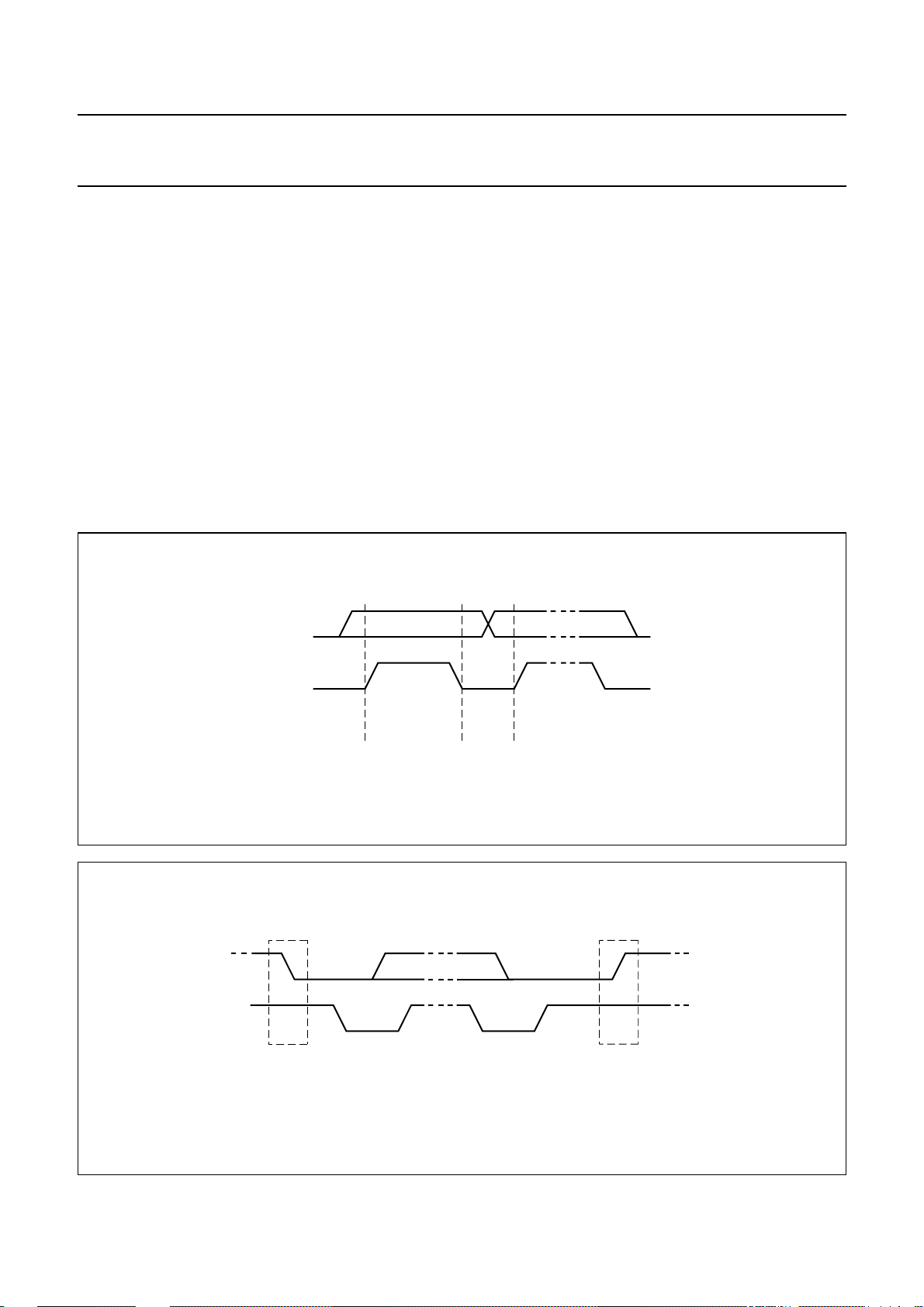
7.1 Bit transfer (see Fig.12)
7.2 START and STOP conditions (see Fig.13)
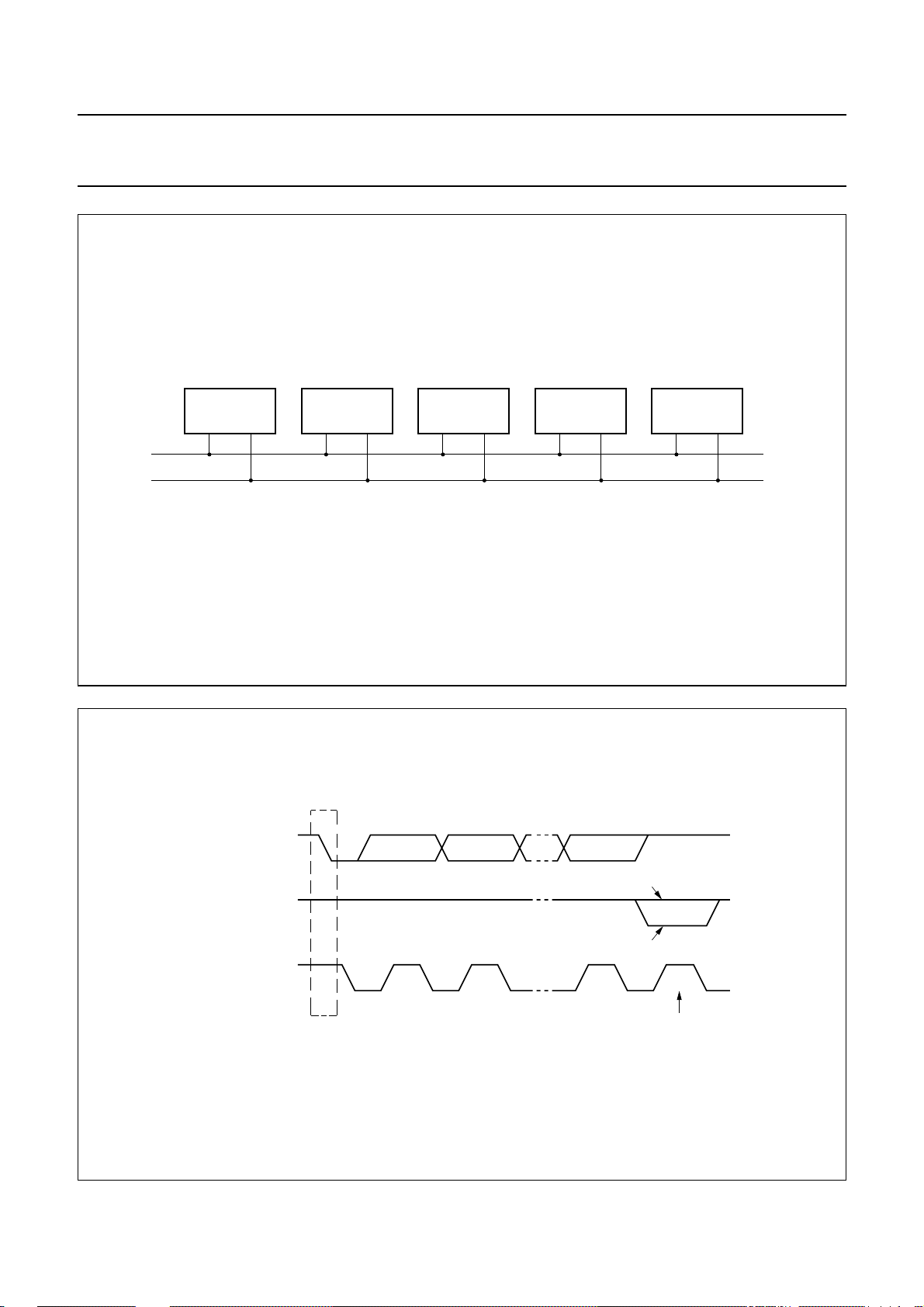
7.3 System configuration (see Fig.14)
7.4 Acknowledge (see Fig.15)
7.5 PCF8576 I2C-bus controller
7.6 Input filters
7.7 I2C-bus protocol
7.8 Command decoder
7.9 Display controller
7.10 Cascaded operation
8 LIMITING VALUES
9 HANDLING
10 DC CHARACTERISTICS
11 AC CHARACTERISTICS
11.1 Typical supply current characteristics
11.2 Typical characteristics of LCD outputs
12 APPLICATION INFORMATION
12.1 Chip-on-glass cascadability in single plane
13 BONDING PAD INFORMATION
14 TRAY INFORMATION: PCF8576U
15 TRAY INFORMATION: PCF8576U/2
16 PACKAGE OUTLINES
17 SOLDERING
17.1 Introduction to soldering surface mount
packages
17.2 Reflow soldering
17.3 Wave soldering
17.4 Manual soldering
17.5 Suitability of surface mount IC packages for
wave and reflow soldering methods
18 DATA SHEET STATUS
19 DEFINITIONS
20 DISCLAIMERS
21 PURCHASE OF PHILIPS I2C COMPONENTS
2001 Oct 02 2
Page 3

Philips Semiconductors Product specification
Universal LCD driver for low multiplex rates PCF8576
1 FEATURES
• Single-chip LCD controller/driver
• Selectable backplanedrive configuration: static or 2/3/4
backplane multiplexing
• Selectable display bias configuration: static,1⁄2 or1⁄
• Internal LCD bias generation with voltage-follower
buffers
• 40 segment drives: up to twenty 8-segment numeric
characters; up to ten 15-segment alphanumeric
characters; or any graphics of up to 160 elements
• 40 × 4-bit RAM for display data storage
• Auto-incremented display data loading across device
subaddress boundaries
• Display memory bank switching in static and duplex
drive modes
• Versatile blinking modes
• LCD and logic supplies may be separated
• Wide power supply range: from 2 V for low-threshold
LCDs and up to 9 V for guest-host LCDs and
high-threshold (automobile) twisted nematic LCDs
• Low power consumption
• Power-saving mode for extremely low power
consumption in battery-operated and telephone
applications
• I2C-bus interface
• TTL/CMOS compatible
• Compatible with any 4-bit, 8-bit or 16-bit
microprocessors/microcontrollers
3
• May be cascaded for large LCD applications (up to
2560 segments possible)
• Cascadable with 24-segment LCD driver PCF8566
• Optimized pinning for plane wiring in both single and
multiple PCF8576 applications
• Space-saving56-leadplasticverysmalloutlinepackage
(VSO56)
• Very low external component count (at most one
resistor, even in multiple device applications)
• Compatible with chip-on-glass technology
• Manufactured in silicon gate CMOS process.
2 GENERAL DESCRIPTION
The PCF8576 is a peripheral device which interfaces to
almost any Liquid Crystal Display (LCD) with low multiplex
rates. It generates the drive signals for any static or
multiplexed LCD containing up to four backplanes and up
to40 segmentsandcaneasily be cascaded for larger LCD
applications. The PCF8576 is compatible with most
microprocessors/microcontrollersandcommunicatesvia a
two-line bidirectional I2C-bus. Communication overheads
are minimized by a display RAM with auto-incremented
addressing, by hardware subaddressing and by display
memory switching (static and duplex drive modes).
3 ORDERING INFORMATION
TYPE NUMBER
NAME DESCRIPTION VERSION
PCF8576T VSO56 plastic very small outline package; 56 leads SOT190-1
PCF8576U − chip in tray −
PCF8576U/2 − chip with bumps in tray −
PCF8576U/5 − unsawn wafer −
PCF8576U/10 FFC chip on film frame carrier (FFC) −
PCF8576U/12 FFC chip with bumps on film frame carrier (FFC) −
2001 Oct 02 3
PACKAGE
Page 4

This text is here in white to force landscape pages to be rotated correctly when browsing through the pdf in the Acrobat reader.This text is here in
_white to force landscape pages to be rotated correctly when browsing through the pdf in the Acrobat reader.This text is here inThis text is here in
white to force landscape pages to be rotated correctly when browsing through the pdf in the Acrobat reader. white to force landscape pages to be ...
2001 Oct 02 4
4 BLOCK DIAGRAM
Philips Semiconductors Product specification
Universal LCD driver for low multiplex rates PCF8576
V
DD
V
LCD
CLK
SYNC
OSC
V
SS
SCL
SDA
5
R
R
LCD BIAS
R
12
4
3
6
11
2
1
GENERATOR
TIMING BLINKER
OSCILLATOR
INPUT
FILTERS
VOLTAGE
SELECTOR
POWER-
ON
RESET
2
I C - BUS
CONTROLLER
LCD
10
BP014BP215BP116BP3
13
BACKPLANE
OUTPUTS
PCF8576
DISPLAY
CONTROLLER
COMMAND
DECODER
INPUT
BANK
SELECTOR
S0 to S39
40
17 to 56
DISPLAY SEGMENT OUTPUTS
DISPLAY LATCH
SHIFT REGISTER
DISPLAY
RAM
40 x 4 BITS
DATA
POINTER
OUTPUT
BANK
SELECTOR
SUBADDRESS
COUNTER
9
SA0
Fig.1 Block diagram (for VSO56 package; SOT190-1).
handbook, full pagewidth
A07A18A2
MBK276
Page 5

Philips Semiconductors Product specification
Universal LCD driver for low multiplex rates PCF8576
5 PINNING
SYMBOL PIN DESCRIPTION
2
SDA 1 I
SCL 2 I
SYNC 3 cascade synchronization input/output
CLK 4 external clock input/output
V
DD
5 supply voltage
OSC 6 oscillator input
A0 to A2 7 to 9 I
SA0 10 I
V
V
SS
LCD
11 logic ground
12 LCD supply voltage
BP0, BP2, BP1 and BP3 13 to 16 LCD backplane outputs
S0 to S39 17 to 56 LCD segment outputs
C-bus serial data input/output
2
C-bus serial clock input
2
C-bus subaddress inputs
2
C-bus slave address input; bit 0
2001 Oct 02 5
Page 6

Philips Semiconductors Product specification
Universal LCD driver for low multiplex rates PCF8576
handbook, halfpage
SDA
SCL
SYNC
CLK
V
DD
OSC
A0
A1
A2
SA0
V
SS
V
LCD
BP0
BP2
BP1
BP3
S0
S1
S2
S3
S4
S5
S6
S7
S8
S9
S10
S11
1
2
3
4
5
6
7
8
9
10
11
12
13
14
PCF8576T
15
16
17
18
19
20
21
22
23
24
25
26
27
28
MBK278
56
S39
55
S38
54
S37
53
S36
52
S35
51
S34
50
S33
49
S32
48
S31
47
S30
46
S29
45
S28
44
S27
43
S26
42
S25
41
S24
40
S23
39
S22
38
S21
37
S20
36
S19
35
S18
34
S17
33
S16
32
S15
31
S14
30
S13
29
S12
Fig.2 Pin configuration; SOT190-1.
2001 Oct 02 6
Page 7

Philips Semiconductors Product specification
Universal LCD driver for low multiplex rates PCF8576
6 FUNCTIONAL DESCRIPTION
The PCF8576 is a versatile peripheral device designed to
interface to any microprocessor/microcontroller to a wide
variety of LCDs. It can directly drive any static or
multiplexed LCD containing up to four backplanes and up
to 40 segments. The display configurations possible with
the PCF8576 depend on the number of active backplane
outputs required; a selection of display configurations is
The host microprocessor/microcontroller maintains the
2-line I2C-bus communication channel with the PCF8576.
The internal oscillator is selected by connecting pin OSC
to pin VSS. The appropriate biasing voltages for the
multiplexed LCD waveforms are generated internally. The
only other connections required to complete the system
are to the power supplies (VDD, VSS and V
) and the
LCD
LCD panel chosen for the application.
given in Table .
All of the display configurations given in Table can be
implemented in the typical system shown in Fig.3.
Selection of display configurations
NUMBER OF 7-SEGMENTS NUMERIC
14-SEGMENTS
ALPHANUMERIC
DOT MATRIX
BACKPLANES SEGMENTS DIGITS
INDICATOR
SYMBOLS
CHARACTERS
INDICATOR
SYMBOLS
4 160 20 20 10 20 160 dots (4 × 40)
3 120 15 15 8 8 120 dots (3 × 40)
2 80 10 10 5 10 80 dots (2 × 40)
1 40552 1240dots (1 × 40)
handbook, full pagewidth
V
DD
HOST
MICRO-
PROCESSOR/
MICRO-
CONTROLLER
V
SS
t
r
R
2C
B
SDA
SCL
OSC
R
OSC
V
DD
512
1 17 to 56
2
PCF8576
6
78
A0 A1 A2SSSA0 V
Fig.3 Typical system configuration.
2001 Oct 02 7
V
LCD
13 to 16
91011
40 segment drives
4 backplanes
LCD PANEL
(up to 160
elements)
MBK277
Page 8

Philips Semiconductors Product specification
Universal LCD driver for low multiplex rates PCF8576
6.1 Power-on reset
At power-on the PCF8576 resets to a starting condition as
follows:
1. All backplane outputs are set to VDD.
2. All segment outputs are set to VDD.
3. Thedrive mode ‘1 : 4 multiplex with1⁄3bias’ is selected.
4. Blinking is switched off.
5. Input and output bank selectors are reset (as defined
in Table 4).
6. The I2C-bus interface is initialized.
7. The data pointer and the subaddress counter are
cleared.
Data transfers on the I2C-bus should be avoided for 1 ms
following power-on to allow completion of the reset action.
6.2 LCD bias generator
The full-scale LCD voltage (Vop) is obtained from
VDD− V
compensatedexternallythroughtheV
. The LCD voltage may be temperature
LCD
supplytopin 12.
LCD
Fractional LCD biasing voltages are obtained from an
internal voltage divider of the three series resistors
connectedbetween VDDandV
.The centre resistor can
LCD
be switched out of the circuit to provide a1⁄2bias voltage
level for the 1 : 2 multiplex configuration.
6.3 LCD voltage selector
The LCD voltage selector co-ordinates the multiplexing of
the LCD in accordance with the selected LCD drive
configuration. The operation of the voltage selector is
controlled by MODE SET commands from the command
decoder. The biasing configurations that apply to the
preferred modes of operation, together with the biasing
characteristics as functions of Vop=VDD− V
LCD
and the
resulting discrimination ratios (D), are given in Table 1.
A practical value for Vopis determined by equating V
off(rms)
with a defined LCD threshold voltage (Vth), typically when
the LCD exhibits approximately 10% contrast. In the static
drive mode a suitable choice is Vop>3Vth approximately.
1
Multiplex drive ratios of 1 : 3 and 1 : 4 with
⁄2bias are
possible but the discrimination and hence the contrast
ratios are smaller ( = 1.732 for 1 : 3 multiplex or
21
= 1.528 for 1 : 4 multiplex).
---------3
3
The advantage of these modes is a reduction of the LCD
full-scale voltage V
• 1 : 3 multiplex (
Vop= = 2.449 V
6V
×
as follows:
op
1
⁄2bias):
off rms〈〉
off(rms)
• 1 : 4 multiplex (1⁄2bias):
43×()
= = 2.309 V
V
op
--------------------- 3
These compare with Vop=3V
off(rms)
when1⁄3bias is used.
off(rms)
Table 1 Preferred LCD drive modes: summary of characteristics
LCD DRIVE MODE
NUMBER OF
BACKPLANES LEVELS
LCD BIAS
CONFIGURATION
V
off(rms)
-------------------- V
op
V
on(rms)
-------------------- V
op
D
static 1 2 static 0 1 ∞
1:2 2 3
1:2 2 4
1:3 3 4
1:4 4 4
1
⁄
2
1
⁄
3
1
⁄
3
1
⁄
3
0.354 0.791 2.236
0.333 0.745 2.236
0.333 0.638 1.915
0.333 0.577 1.732
V
=
-------------------- V
on(rms)
off(rms)
2001 Oct 02 8
Page 9
Philips Semiconductors Product specification
Universal LCD driver for low multiplex rates PCF8576
6.4 LCD drive mode waveforms
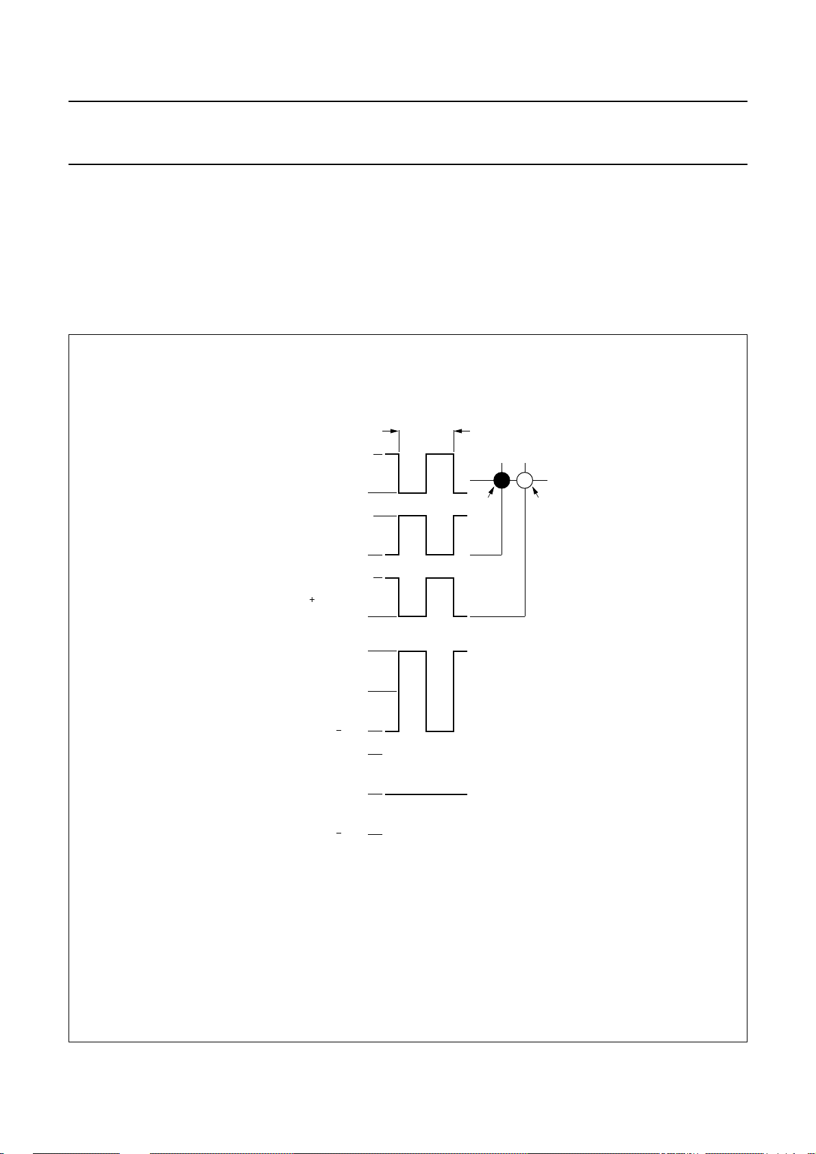
The static LCD drive mode is used when a single
backplaneisprovidedintheLCD.Backplaneandsegment
drive waveforms for this mode are shown in Fig.4.
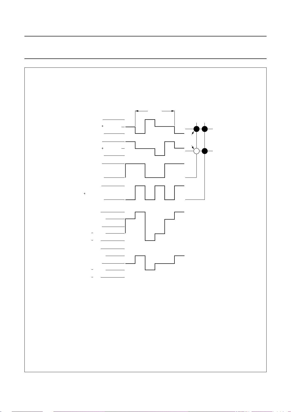
When two backplanes are provided in the LCD, the 1 : 2
multiplex mode applies. The PCF8576 allows use of
1
⁄2bias or1⁄3bias in this mode as shown in Figs 5 and 6.
V
DD
BP0
V
LCD
V
DD
S
n
V
LCD
V
DD
S
n 1
V
LCD
(a) waveforms at driver
V
op
When three backplanes are provided in the LCD, the 1 : 3
multiplex drive mode applies, as shown in Fig.7.
When four backplanes are provided in the LCD, the 1 : 4
multiplex drive mode applies, as shown in Fig.8.
T
frame
LCD segments
state 1
(on)
state 2
(off)
state 1 0
V
op
V
op
state 2 0
V
op
(b) resultant waveforms
at LCD segment
V
t() V
t() V
state1
V
on(rms)Vop
t() V
V
state2
V
off(rms)
S
n
=
S
n1+
0V=
BP0
t() V
BP0
t()–=
t()–=
Fig.4 Static drive mode waveforms (Vop=VDD− V
2001 Oct 02 9
MBE539
LCD
).
Page 10
Philips Semiconductors Product specification
Universal LCD driver for low multiplex rates PCF8576
T
frame
V
(V )/2V
BP0
V
V
(V )/2V
BP1
V
V
S
n
V
V
S
n 1
V
V
V /2
state 1 0
V /2
V
V
V /2
state 2
V /2
V
DD
DD LCD
LCD
DD
LCD
DD
LCD
DD
LCD
DD
LCD
op
op
op
op
op
op
0
op
op
(a) waveforms at driver
(b) resultant waveforms
at LCD segment
LCD segments
state 1
state 2
MBE540
V
t() V
t() V
op
t() V
op
BP0
BP1
t()–=
t()–=
state1
V
on(rms)
V
state2
V
off(rms)
0.791V
=
t() V
0.354V
=
S
n
S
n
Fig.5 Waveforms for the 1 : 2 multiplex drive mode with1⁄2bias (Vop=VDD− V
2001 Oct 02 10
LCD
).
Page 11

Philips Semiconductors Product specification
Universal LCD driver for low multiplex rates PCF8576
T
V
DD
V V /3
BP0
BP1
S
n
S
n 1
state 1 0
state 2 0
DD
V 2V /3
DD
V
LCD
V
DD
V V /3
DD
V 2V /3
DD
V
LCD
V
DD
V V /3
DD
V 2V /3
DD
V
LCD
V
DD
V V /3
DD
V 2V /3
DD
V
LCD
V
op
2V /3
op
V /3
op
V /3
op
2V /3
op
V
op
V
op
2V /3
op
V /3
op
V /3
op
2V /3
op
V
op
op
op
op
op
op
op
op
op
frame
(a) waveforms at driver
(b) resultant waveforms
at LCD segment
LCD segments
state 1
state 2
MBE541
V
t() V
t() V
op
t() V
op
BP0
BP1
t()–=
t()–=
state1
V
on(rms)
V
state2
V
off(rms)
0.745V
=
t() V
0.333V
=
S
n
S
n
Fig.6 Waveforms for the 1 : 2 multiplex drive mode with1⁄3bias (Vop=VDD− V
2001 Oct 02 11
LCD
).
Page 12

Philips Semiconductors Product specification
Universal LCD driver for low multiplex rates PCF8576
T
V
V V /3
BP0
V 2V /3
V
V
V V /3
BP1
V 2V /3
V
V
BP2/S23
V V /3
V 2V /3
V
V
V V /3
S
n
V 2V /3
V
V
n 1
V V /3
V 2V /3
S
V
V
n 2
V V /3
V 2V /3
S
V
V
2V /3
V /3
state 1 0
V /3
2V /3
V
V
2V /3
V /3
state 2 0
V /3
2V /3
V
DD
DD
DD
LCD
DD
DD
DD
LCD
DD
DD
DD
LCD
DD
DD
DD
LCD
DD
DD
DD
LCD
DD
DD
DD
LCD
op
op
op
op
op
op
op
op
op
op
op
op
op
op
op
op
op
op
op
op
op
op
op
op
frame
(a) waveforms at driver
(b) resultant waveforms
at LCD segment
LCD segments
state 1
state 2
MBE542
V
t() V
t() V
op
t() V
op
BP0
BP1
t()–=
t()–=
state1
V
on(rms)
V
state2
V
off(rms)
0.638V
=
t() V
0.333V
=
S
n
S
n
Fig.7 Waveforms for the 1 : 3 multiplex drive mode (Vop=VDD− V
2001 Oct 02 12
LCD
).
Page 13

Philips Semiconductors Product specification
Universal LCD driver for low multiplex rates PCF8576
T
V
DD
V V /3
n
DD
V 2V /3
DD
V
LCD
V
DD
V V /3
DD
V 2V /3
DD
V
LCD
V
DD
V V /3
DD
V 2V /3
DD
V
LCD
V
DD
V V /3
DD
V 2V /3
DD
V
LCD
V
DD
V V /3
DD
V 2V /3
DD
V
LCD
V
DD
V V /3
DD
V 2V /3
DD
V
LCD
V
DD
V V /3
DD
V 2V /3
DD
V
LCD
V
DD
V V /3
DD
V 2V /3
DD
V
LCD
V
op
2V /3
op
V /3
op
V /3
op
2V /3
op
V
op
V
op
2V /3
op
V /3
op
V /3
op
2V /3
op
V
op
BP0
BP1
BP2
BP3
S
S
n 1
S
n 2
S
n 3
state 1 0
state 2 0
op
op
op
op
op
op
op
op
op
op
op
op
op
op
op
op
frame
(a) waveforms at driver
(b) resultant waveforms
at LCD segment
state 1
state 2
LCD segments
MBE543
V
state1
V
on(rms)
V
state2
V
off(rms)
t() V
0.577V
=
t() V
0.333V
=
S
S
t() V
n
t() V
n
t()–=
BP0
op
t()–=
BP1
op
Fig.8 Waveforms for the 1 : 4 multiplex drive mode (Vop=VDD− V
2001 Oct 02 13
LCD
).
Page 14
Philips Semiconductors Product specification
Universal LCD driver for low multiplex rates PCF8576
6.5 Oscillator
6.5.1 INTERNAL CLOCK The internal logic and the LCD drive signals of the
PCF8576 are timed either by the internal oscillator or from
an external clock. When the internal oscillator is used,
pin OSC should be connected to pin VSS. In this event, the
output from pin CLK provides the clock signal for
cascaded PCF8566s in the system.
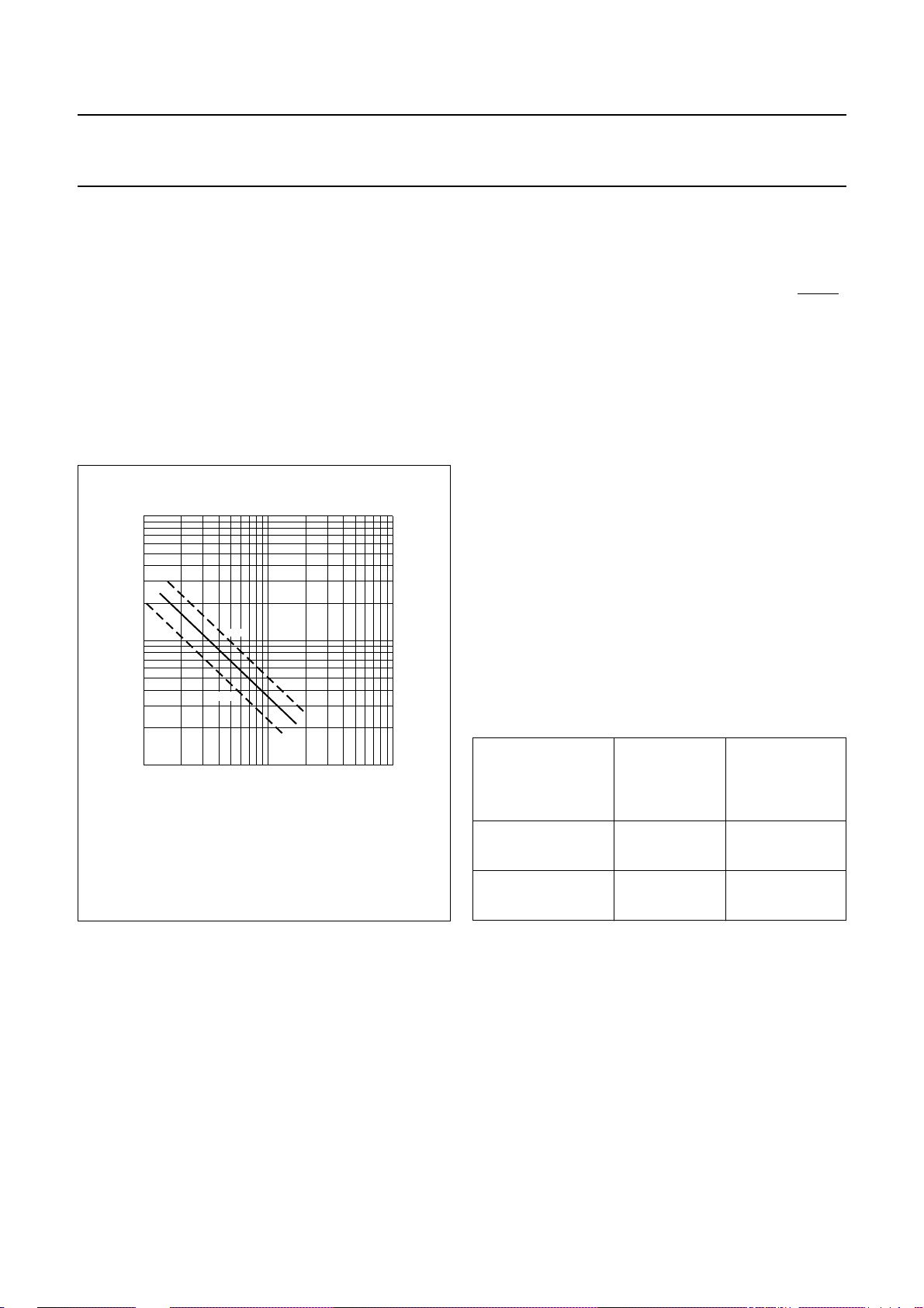
WhereresistorR
toVSSispresent,theinternaloscillator
osc
is selected. The relationship between the oscillator
frequency on pin CLK (f
3
10
f
clk
(kHz)
2
10
min
) and R
clk
max
is shown in Fig.9.
osc
MBE531
6.6 Timing
ThetimingofthePCF8576organizestheinternaldataflow
of the device. This includes the transfer of display data
from the display RAM to the display segment outputs. In
cascaded applications, the synchronization signal
SYNC
maintains the correct timing relationship between the
PCF8576s in the system. The timing also generates the
LCD frame frequency which it derives as an integer
multiple of the clock frequency (see Table 2). The frame
frequency is set by the MODE SET commands when
internal clock is used, or by the frequency applied to
pin CLK when external clock is used.
The ratio between the clock frequency and the LCD frame
frequency depends on the mode in which the device is
operating. In the power-saving mode the reduction ratio is
six times smaller; this allows the clock frequency to be
reduced by a factor of six. The reduced clock frequency
results in a significant reduction in power dissipation. The
lower clock frequency has the disadvantage of increasing
the response time when large amounts of display data are
transmitted on the I2C-bus.
When a device is unable to digest a display data byte
beforethe next one arrives, it holds the SCL line LOW until
the first display data byte is stored. This slows down the
transmission rate of the I2C-bus but no data loss occurs.
10
2
10
3.4 107×
f
----------------------- -
clk
R
osc
kHz()≈
3
10
R(kΩ)
osc
Fig.9 Oscillator frequency as a function of R
6.5.2 E
XTERNAL CLOCK
4
10
.
osc
The condition for external clock is made by connecting
pin OSC to pin VDD; pin CLK then becomes the external
clock input.
The clock frequency (f
) determines the LCD frame
clk
frequency and the maximum rate for data reception from
the I2C-bus. To allow I2C-bus transmissions at their
maximumdata rate of 100 kHz, f
shouldbe chosen to be
clk
above 125 kHz.
A clock signal must always be supplied to the device;
removing the clock may freeze the LCD in a DC state.
Table 2 LCD frame frequencies
NOMINAL
PCF8576 MODE
FRAME
FREQUENCY
FRAME
FREQUENCY
(Hz)
f
Normal mode
Power-saving mode 64
clk
------------ 2880
f
clk
--------- 480
64
6.7 Display latch
The display latch holds the display data while the
corresponding multiplex signals are generated. There is a
one-to-one relationship between the data in the display
latch, the LCD segment outputs and one column of the
display RAM.
6.8 Shift register
The shift register serves to transfer display information
from the display RAM to the display latch while previous
data is displayed.
2001 Oct 02 14
Page 15

Philips Semiconductors Product specification
Universal LCD driver for low multiplex rates PCF8576
6.9 Segment outputs
The LCD drive section includes 40 segment outputs
pins S0 to S39 which should be connected directly to the
LCD. The segment output signals are generated in
accordance with the multiplexed backplane signals and
with data resident in the display latch. When less than
40 segment outputs are required the unused segment
outputs should be left open-circuit.
6.10 Backplane outputs
The LCD drive section includes four backplane outputs
BP0 to BP3 which should be connected directly to the
LCD. The backplane output signals are generated in
accordance with the selected LCD drive mode.If less than
four backplane outputs are required the unused outputs
can be left open-circuit. In the 1 : 3 multiplex drive mode
BP3 carries the same signal as BP1, therefore these two
adjacent outputs can be connected together to give
enhanced drive capabilities. In the 1 : 2 multiplex drive
mode BP0 and BP2, BP1 and BP3 respectively carry the
same signals and may also be paired to increase the drive
capabilities. In the static drive mode the same signal is
carried by all four backplane outputs and they can be
connected in parallel for very high drive requirements.
6.11 Display RAM
The display RAM is a static 40 × 4-bit RAM which stores
LCD data. A logic 1 in the RAM bit-map indicates the on
state of the corresponding LCD segment; similarly, a
logic 0 indicates the off state. There is a one-to-one
correspondence between the RAM addresses and the
segmentoutputs,andbetweentheindividualbitsofaRAM
word and the backplane outputs. The first RAM column
corresponds to the 40 segments operated with respect to
backplane BP0 (see Fig.10). In multiplexed LCD
applications the segment data of the second, third and
fourth column of the display RAM are time-multiplexed
with BP1, BP2 and BP3 respectively.
When display data is transmitted to the PCF8576 the
display bytes received are stored in the display RAM in
accordance with the selected LCD drive mode. To
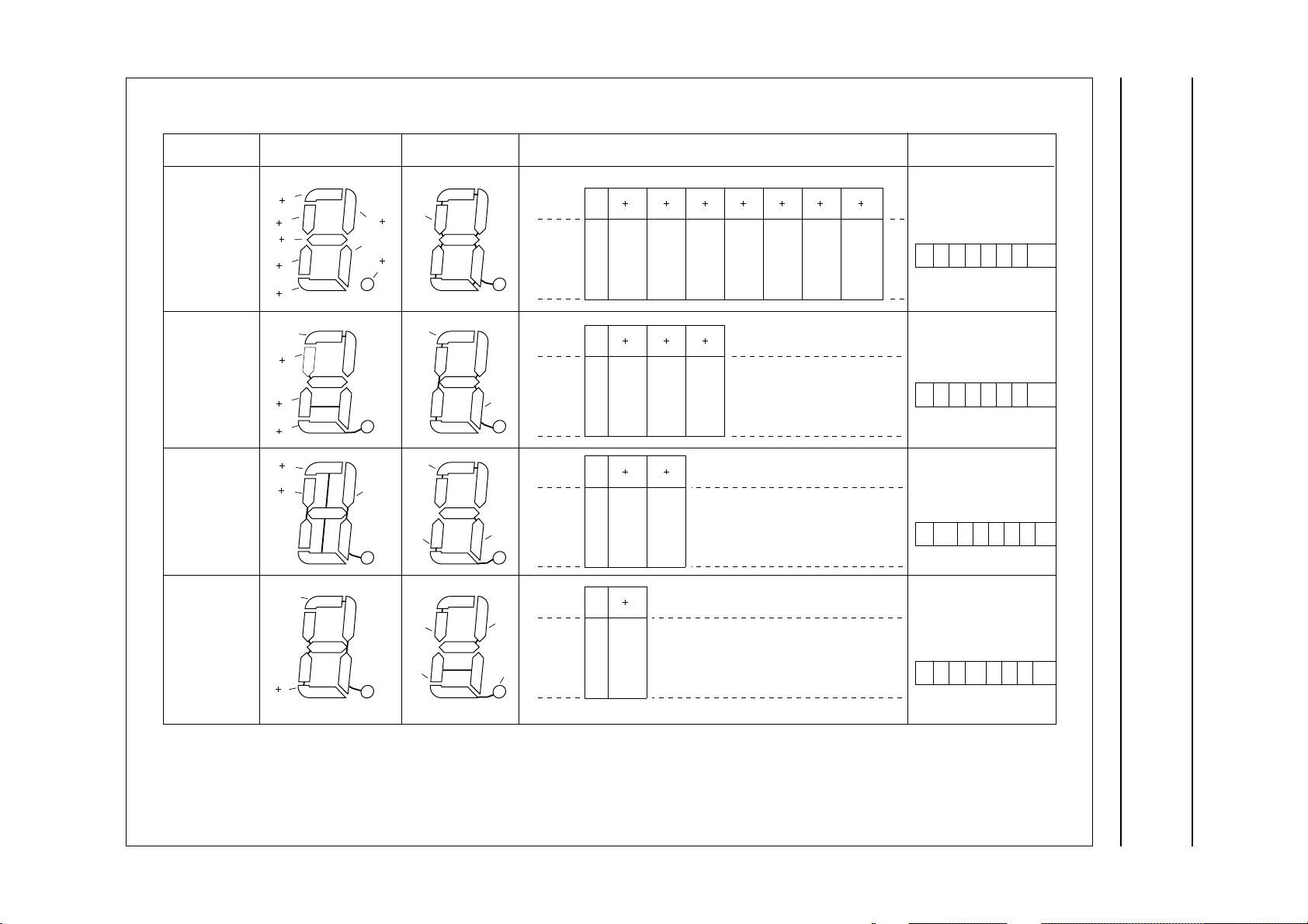
illustrate the filling order, an example of a 7-segment
numericdisplay showing all drive modes is given inFig.11;
the RAM filling organization depicted applies equally to
other LCD types.
With reference to Fig.11, in the static drive mode the eight
transmitteddata bits are placed in bit 0 of eight successive
display RAM addresses. In the 1 : 2 multiplex drive mode
the eight transmitted data bits are placed in bits 0 and 1 of
four successive display RAM addresses. In the 1 : 3
multiplex drive mode these bits are placed in
bits 0, 1 and 2 of three successive addresses, with bit 2 of
the third address left unchanged. This last bit may, if
necessary, be controlled by an additional transfer to this
address but care should be taken to avoid overriding
adjacentdatabecausefullbytesarealwaystransmitted.In
the 1 : 4 multiplex drive mode the eight transmitted data
bits are placed in bits 0, 1, 2 and 3 of two successive
display RAM addresses.
display RAM addresses (rows) / segment outputs (S)
1234 3536373839
0
0
display RAM bits
(columns) /
backplane outputs
(BP)
1
2
3
MBE525
Fig.10 Display RAM bit-map showing direct relationship between display RAM addresses and segment outputs,
and between bits in a RAM word and backplane outputs.
2001 Oct 02 15
Page 16

Philips Semiconductors Product specification
Universal LCD driver for low multiplex rates PCF8576
6.12 Data pointer
The addressing mechanism for the display RAM is
realized using the data pointer. This allows the loading of
an individual display data byte, or a series of display data
bytes, into any location of the display RAM. The sequence
commenceswith the initialization of thedata pointer by the
LOAD DATA POINTER command. Following this, an
arriving data byte is stored starting at the display RAM
address indicated by the data pointer thereby observing
the filling order shown in Fig.11. The data pointer is
automatically incremented in accordance with the chosen
LCD configuration. That is, after each byte is stored, the
contents of the data pointer are incremented by eight
(static drive mode), by four (1 : 2 multiplex drive mode) or
by two (1 : 4 multiplex drive mode).
6.13 Subaddress counter
The storage of display data is conditioned by the contents
of the subaddress counter. Storage is allowed to take
place only when the contents of the subaddress counter
agree with the hardware subaddress applied to A0, A1
and A2. The subaddress counter value is defined by the
DEVICE SELECT command. If the contents of the
subaddress counter and the hardware subaddress do not
agree then data storage is inhibited but the data pointer is
incremented as if data storage had taken place. The
subaddress counter is also incremented when the data
pointer overflows.
6.14 Output bank selector
This selects one of the four bits per display RAM address
for transfer to the display latch. The actual bit chosen
depends on the particular LCD drive mode in operation
and on the instant in the multiplex sequence. In 1 : 4
multiplex, all RAM addresses of bit 0 are the first to be
selected, these are followed by the contents of bit 1, bit 2
and then bit 3. Similarly in 1 : 3 multiplex, bits 0, 1 and 2
are selected sequentially. In 1 : 2 multiplex, bits 0 and 1
are selected and, in the static mode, bit 0 is selected.
The PCF8576 includes a RAM bank switching feature in
the static and 1 : 2 multiplex drive modes. In the static
drive mode, the BANK SELECT command may request
the contents of bit 2 to be selected for display instead of
bit 0 contents. In the 1 : 2 drive mode, the contents of
bits 2 and 3 may be selected instead of bits 0 and 1. This
gives the provision for preparing display information in an
alternative bank and to be able to switch to it once it is
assembled.
6.15 Input bank selector
The input bank selector loads display data into the display
RAM in accordance with the selected LCD drive
configuration. Display data can be loaded in bit 2 in static
drive mode or in bits 2 and 3 in 1 : 2 drive mode by using
the BANK SELECT command. The input bank selector
functions independent of the output bank selector.
The storage arrangements described lead to extremely
efficient data loading in cascaded applications. When a
series of display bytes are sent to the display RAM,
automatic wrap-over to the next PCF8576 occurs when
the last RAM address is exceeded. Subaddressing across
device boundaries is successful even if the change to the
next device in the cascade occurs within a transmitted
character (such as during the 14th display data byte
transmitted in 1 : 3 multiplex mode).
2001 Oct 02 16
Page 17

Philips Semiconductors Product specification
Universal LCD driver for low multiplex rates PCF8576
6.16 Blinker
The display blinking capabilities of the PCF8576 are very
versatile. The whole display can be blinked at frequencies
selectedbytheBLINKcommand.The blinking frequencies
are integer multiples of the clock frequency; the ratios
between the clock and blinking frequencies depend on the
mode in which the device is operating, as shown in
Table 3.
An additional feature is for an arbitrary selection of LCD
segments to be blinked. This applies to the static and
1 : 2 LCD drive modes and can be implemented without
any communication overheads. By means of the output
Table 3 Blinking frequencies
BLINKING MODE
NORMAL OPERATING
MODE RATIO
Off −−blinking off
f
2Hz 2Hz
1Hz 1Hz
clk
---------------92160
f
clk
------------------- 184320
bank selector, the displayed RAM banks are exchanged
with alternate RAM banks at the blinking frequency. This
mode can also be specified by the BLINK command.
In the 1 : 3 and 1 : 4 multiplex modes, where no alternate
RAM bank is available, groups of LCD segments can be
blinked by selectively changing the display RAM data at
fixed time intervals.
If the entire display is to be blinked at a frequency other
thanthe nominal blinking frequency, this canbe effectively
performed by resetting and settingthe display enable bit E
at the required rate using the MODE SET command.
POWER-SAVING MODE
RATIO
f
clk
---------------15360
f
clk
---------------30720
NOMINAL BLINKING
FREQUENCY
f
0.5 Hz 0.5 Hz
clk
------------------- 368640
f
clk
---------------61440
2001 Oct 02 17
Page 18
This text is here in white to force landscape pages to be rotated correctly when browsing through the pdf in the Acrobat reader.This text is here in
_white to force landscape pages to be rotated correctly when browsing through the pdf in the Acrobat reader.This text is here inThis text is here in
white to force landscape pages to be rotated correctly when browsing through the pdf in the Acrobat reader. white to force landscape pages to be ...
2001 Oct 02 18
Philips Semiconductors Product specification
Universal LCD driver for low multiplex rates PCF8576
drive mode
static
1 : 2
multiplex
1 : 3
multiplex
1 : 4
multiplex
LCD segments LCD backplanes display RAM filling order transmitted display byte
S
n
S
n
S
n
S
n
S
n
S
n
S
n
S
n
S
n
S
n
S
n
a
2
3
4
5
6
S
n
1
2
3
1
2
S
n
1
b
f
g
e
c
d
a
b
f
g
e
c
d
a
b
f
g
e
c
d
a
b
f
g
e
c
d
BP0
S
1
n
S
n
S
7
n
DP
BP0
bit/
BP
bit/
BP1
DP
BP0
S
n
BP
bit/
BP
DP
BP1
BP0
BP2
BP2
bit/
BP
BP1
DP
BP3
n1
n
c
0
x
1
x
2
x
3
n
a
0
b
1
x
2
x
3
n
b
0
DP
1
c
2
x
3
n
a
0
c
1
b
2
DP
3
n2 n3 n4 n5 n6 n7
b
a
f
g
e
x
x
x
x
x
x
n1
f
g
x
x
n1
a
d
g
x
x
x
x
x
n2 n3
e
d
c
DP
x
x
x
x
n2
f
e
x
x
x
x
x
x
x
n1
f
e
g
d
d
DP
x
x
x
x
x
x
MSB LSB
cbaf gedDP
MSB LSB
abf gecdDP
MSB LSB
bDPcadgf e
MSB LSB
acbDPf egd
x = data bit unchanged.
Fig.11 Relationships between LCD layout, drive mode, display RAM filling order and display data transmitted over the I2C-bus.
MBK389
handbook, full pagewidth
Page 19

Philips Semiconductors Product specification
Universal LCD driver for low multiplex rates PCF8576
7 CHARACTERISTICS OF THE I2C-BUS
The I2C-bus is for bidirectional, two-line communication
between different ICs or modules. The two lines are a
serial data line (SDA) and a serial clock line (SCL). Both
lines must be connected to a positive supply via a pull-up
resistor when connected to the output stages of a device.
Data transfer may be initiated only when the bus is not
busy.
7.1 Bit transfer (see Fig.12) One data bit is transferred during each clock pulse. The
data on the SDA line must remain stable during the HIGH
period of the clock pulse as changes in the data line at this
time will be interpreted as a control signal.
7.2 START and STOP conditions (see Fig.13) Bothdataand clock lines remain HIGH when the bus is not
busy. A HIGH-to-LOW transition of the data line, while the
clock is HIGH is defined as the START condition (S). A
LOW-to-HIGH transition of the data line while the clock is
HIGH is defined as the STOP condition (P).
7.3 System configuration (see Fig.14)
7.5 PCF8576 I2C-bus controller
The PCF8576 acts as an I2C-bus slave receiver. It does
not initiate I2C-bus transfers or transmit data to an I2C-bus
master receiver. The only data output from the PCF8576
are the acknowledge signals of the selected devices.
Device selection depends on the I2C-bus slave address,
on the transferred command data and on the hardware
subaddress.
In single device application, the hardware subaddress
inputsA0, A1 and A2 are normally connected to VSSwhich
defines the hardware subaddress 0. In multiple device
applications A0, A1 and A2 are connected to VSSor VDDin
accordance with a binary coding scheme such that no two
devices with a common I2C-bus slave address have the
same hardware subaddress.
In the power-saving mode it is possible that the PCF8576
is not able to keep up with the highest transmission rates
when large amounts of display data are transmitted. If this
situation occurs, the PCF8576 forces the SCLline to LOW
until its internal operations are completed. This is known
as the ‘clock synchronization feature’ of the I2C-bus and
serves to slow down fast transmitters. Data loss does not
occur.
A device generating a message is a ‘transmitter’, a device
receiving a message is the ‘receiver’. The device that
controlsthemessageisthe‘master’andthedeviceswhich
are controlled by the master are the ‘slaves’.
7.4 Acknowledge (see Fig.15) The number of data bytestransferred between the START
and STOP conditions from transmitter to receiver is
unlimited. Each byte of eight bits is followed by an
acknowledge bit. The acknowledge bit is a HIGH level
signal put on the bus by the transmitter during which time
the master generates an extra acknowledge related clock
pulse. A slave receiver which is addressed must generate
an acknowledge after the reception of each byte. Also a
master receiver must generate an acknowledge after the
reception of each byte that has been clocked out of the
slave transmitter. The device that acknowledges must
pull-down the SDA line during the acknowledge clock
pulse, so that the SDA line is stable LOW during the HIGH
period of the acknowledge related clock pulse (set-up and
hold times must be taken into consideration). A master
receiver must signal an end of data to the transmitter by
not generating an acknowledge on the last byte that has
been clocked out of the slave. In this event the transmitter
must leave the data line HIGH to enable the master to
generate a STOP condition.
7.6 Input filters
To enhance noise immunity in electrically adverse
environments, RC low-pass filters are provided on the
SDA and SCL lines.
7.7 I
TwoI2C-busslaveaddresses(0111000 and 0111001)are
reserved for the PCF8576. The least significant bit of the
slaveaddress that a PCF8576 will respond toisdefined by
the level connected at its input pin SA0. Therefore, two
types of PCF8576 can be distinguished on the same
I2C-bus which allows:
• Up to 16 PCF8576s on the same I2C-bus for very large
• The use of two types of LCD multiplex on the same
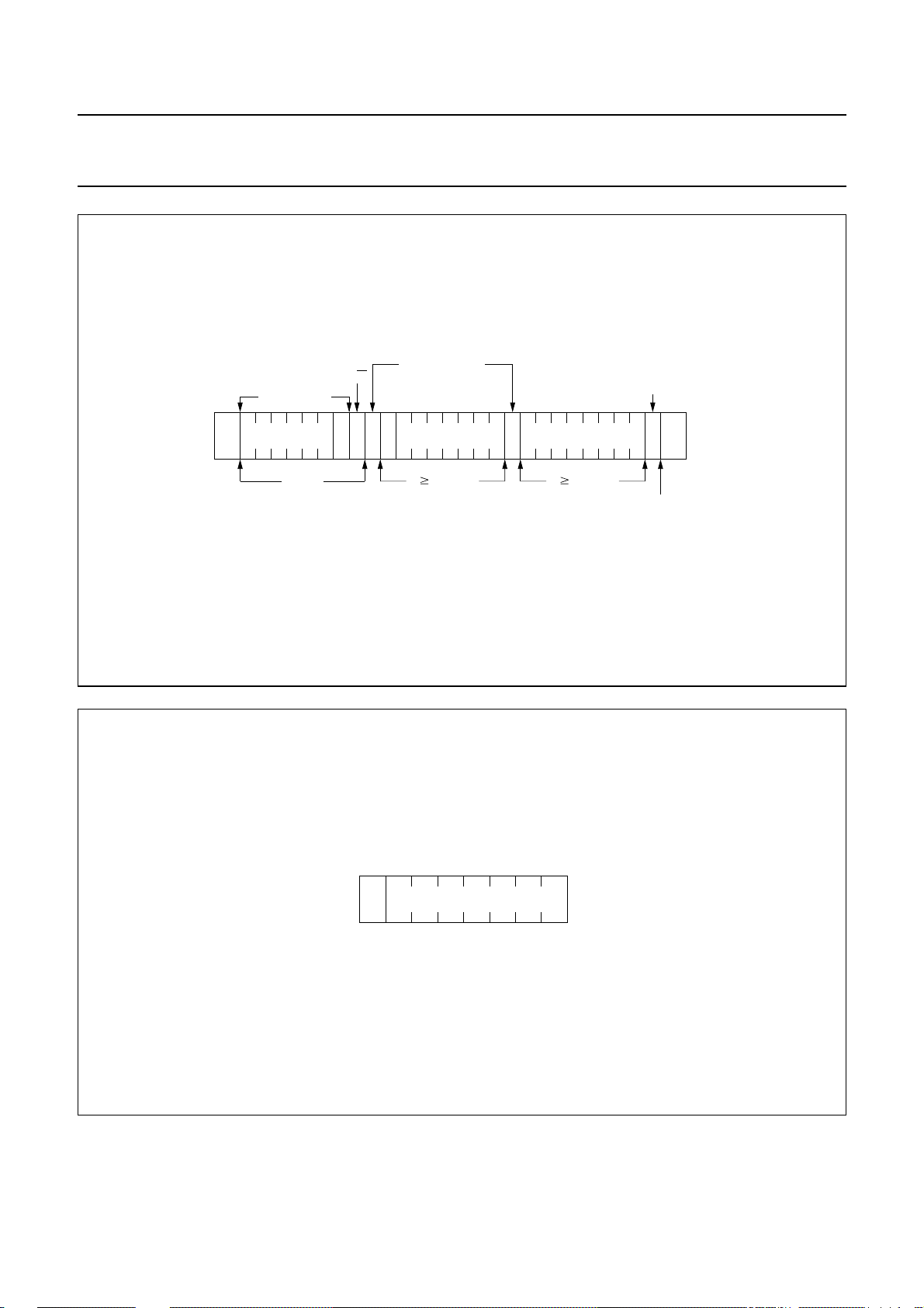
The I2C-bus protocol is shown in Fig.16. The sequence is
initiated with a START condition (S) from the I2C-bus
master which is followed by one of the two PCF8576 slave
addressesavailable.AllPCF8576swiththecorresponding
SA0 level acknowledge in parallel with the slave address
but all PCF8576s with the alternative SA0 level ignore the
whole I2C-bus transfer.
2
C-bus protocol
LCD applications
I2C-bus.
2001 Oct 02 19
Page 20
Philips Semiconductors Product specification
Universal LCD driver for low multiplex rates PCF8576
After acknowledgement, one or more command bytes (m)
follow which define the statusof the addressed PCF8576s.
The last command byte is tagged with a cleared most
significant bit, the continuation bit C. The command bytes
arealso acknowledged by all addressed PCF8576son the
bus.
After the last command byte, a series of display data bytes
(n) may follow. These display bytes are stored in the
display RAM at the address specified by the data pointer
and the subaddress counter. Both data pointer and
subaddress counter are automatically updated and the
data is directed to the intended PCF8576 device. The
acknowledgementafter each byte is made only by the (A0,
A1 and A2) addressed PCF8576. After the last display
byte, the I2C-bus master issues a STOP condition (P).
SDA
7.8 Command decoder
The command decoder identifies command bytes that
arrive on the I2C-bus. All available commands carry a
continuation bit C in their most significant bit position
(Fig.17). When this bit is set, it indicates that the next byte
of the transfer to arrive will also represent a command. If
this bit is reset, it indicates the last command byte of the
transfer. Further bytes will be regarded as display data.
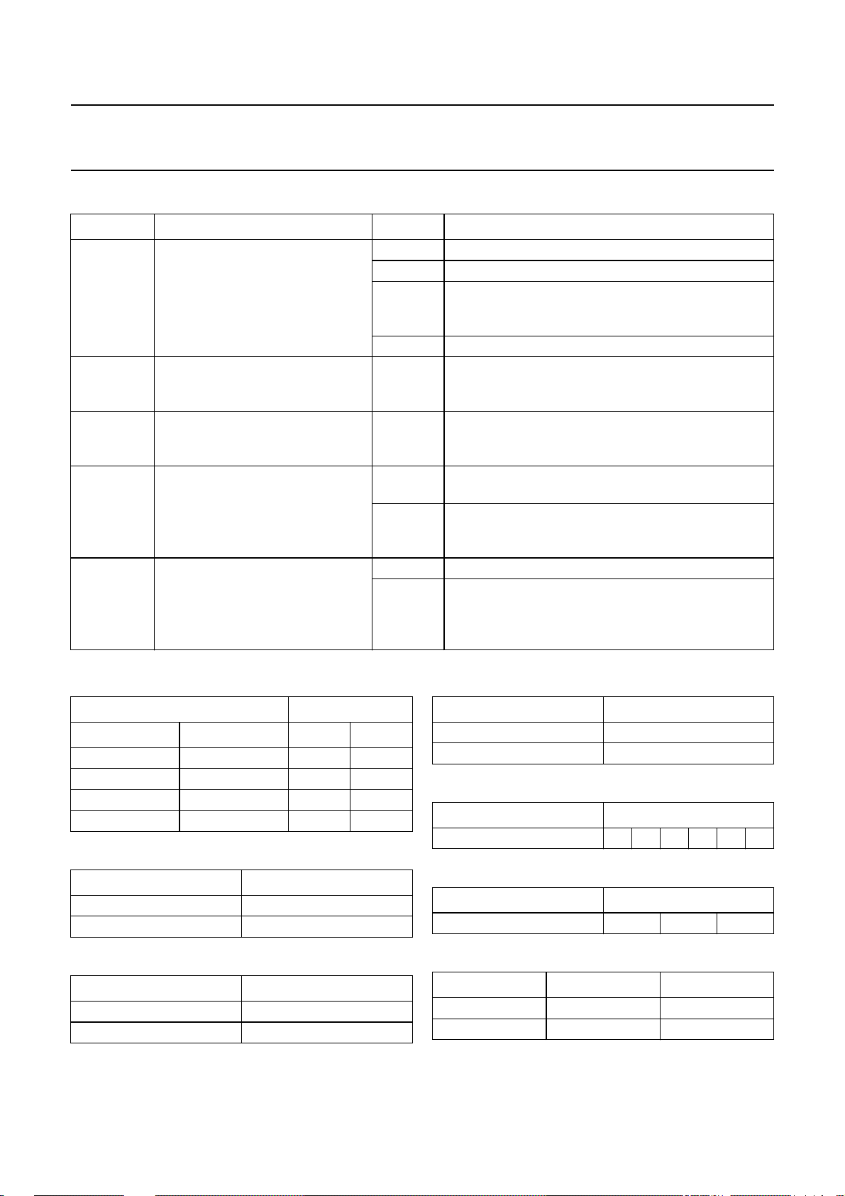
The five commands available to the PCF8576 are defined
in Table 4.
handbook, full pagewidth
SDA
SCL
SCL
S
START condition
data line
stable;
data valid
change
of data
allowed
Fig.12 Bit transfer.
MBA607
P
STOP condition
SDA
SCL
MBC622
Fig.13 Definition of START and STOP conditions.
2001 Oct 02 20
Page 21
Philips Semiconductors Product specification
Universal LCD driver for low multiplex rates PCF8576
SDA
SCL
handbook, full pagewidth
MASTER
TRANSMITTER/
RECEIVER
DATA OUTPUT
BY TRANSMITTER
SLAVE
RECEIVER
SLAVE
TRANSMITTER/
RECEIVER
TRANSMITTER
Fig.14 System configuration.
MASTER
MASTER
TRANSMITTER/
RECEIVER
MGA807
DATA OUTPUT
BY RECEIVER
SCL FROM
MASTER
S
START
condition
Fig.15 Acknowledgement on the I2C-bus.
2001 Oct 02 21
not acknowledge
acknowledge
acknowledgement
9821
clock pulse for
MBC602
Page 22
Philips Semiconductors Product specification
Universal LCD driver for low multiplex rates PCF8576
handbook, full pagewidth
slave address
S
011100 0AC
S
A
0
acknowledge by
all addressed
/RW
PCF8576s
COMMAND
Fig.16 I2C-bus protocol.
acknowledge
by A0, A1 and A2
selected
PCF8576 only
A
n 0 byte(s)n 1 byte(s)1 byte
MBK279
ADISPLAY DATA
P
update data pointers
and if necessary,
subaddress counter
MSB LSB
C
C = 0; last command.
C = 1; commands continue.
REST OF OPCODE
Fig.17 General format of command byte.
2001 Oct 02 22
MSA833
Page 23
Philips Semiconductors Product specification
Universal LCD driver for low multiplex rates PCF8576
Table 4 Definition of PCF8576 commands
COMMAND OPCODE OPTIONS DESCRIPTION
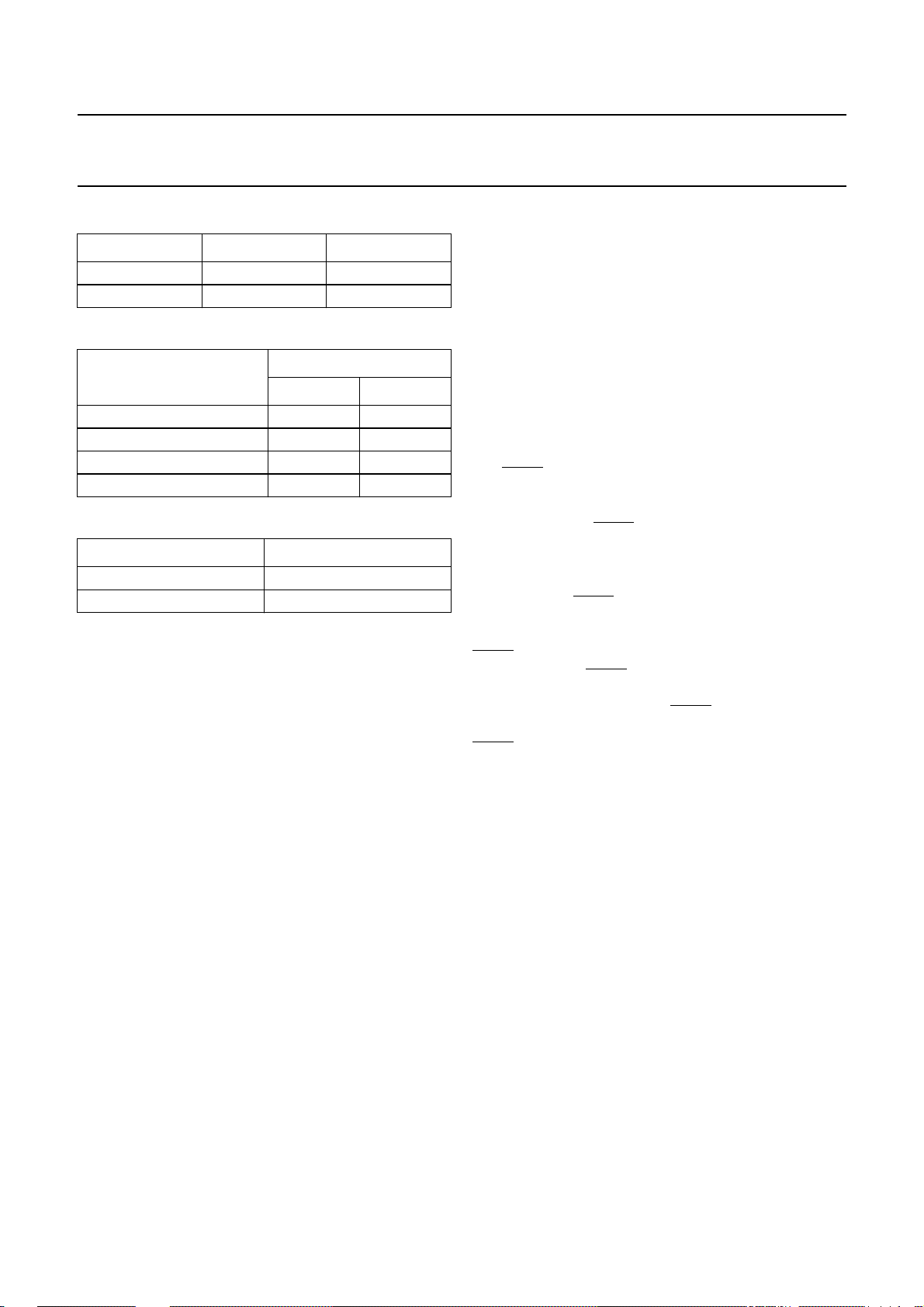
MODE SET C 1 0 LP E B M1 M0 Table 5 Defines LCD drive mode.
Table 6 Defines LCD bias configuration.
Table 7 Defines display status. The possibility to disable the
display allows implementation of blinking under
external control.
Table 8 Defines power dissipation mode.
LOADDATA
POINTER
DEVICE
SELECT
BANK
SELECT
BLINK C 1 1 1 0 A BF1 BF0 Table 13 Defines the blinking frequency.
C 0 P5 P4 P3 P2 P1 P0 Table 9 Six bits of immediate data, bits P5 to P0, are
transferred to the data pointer to define one of forty
display RAM addresses.
C 1 1 0 0 A2 A1 A0 Table 10 Three bits of immediate data, bits A2 to A0, are
transferred to the subaddress counter to define one of
eight hardware subaddresses.
C11110 I O Table11Defines input bank selection (storage of arriving
display data).
Table 12 Defines output bank selection (retrievalof LCD display
data). The BANK SELECT command has no effect in
1 : 3 and 1 : 4 multiplex drive modes.
Table 14 Selects the blinking mode; normal operation with
frequency set byBF1, BF0 or blinking by alternation of
display RAM banks. Alternation blinking does not
apply in 1 : 3 and 1 : 4 multiplex drive modes.
Table 5 MODE SET option 1
LCD DRIVE MODE BITS
DRIVE MODE BACKPLANE M1 M0
Static 1 BP 0 1
1 : 2 MUX (2 BP) 1 0
1 : 3 MUX (3 BP) 1 1
1 : 4 MUX (4 BP) 0 0
Table 6 MODE SET option 2
LCD BIAS BIT B
1
⁄3bias 0
1
⁄2bias 1
Table 7 MODE SET option 3
DISPLAY STATUS BIT E
Disabled (blank) 0
Enabled 1
Table 8 MODE SET option 4
MODE BIT LP
Normal mode 0
Power-saving mode 1
Table 9 LOAD DATA POINTER option 1
DESCRIPTION BITS
6-bit binary value of 0 to 39 P5 P4 P3 P2 P1 P0
Table 10 DEVICE SELECT option 1
DESCRIPTION BITS
3-bit binary value of 0 to 7 A2 A1 A0
Table 11 BANK SELECT option 1
STATIC 1 : 2 MUX BIT I
RAM bit 0 RAM bits 0 and 1 0
RAM bit 2 RAM bits 2 and 3 1
2001 Oct 02 23
Page 24
Philips Semiconductors Product specification
Universal LCD driver for low multiplex rates PCF8576
Table 12 BANK SELECT option 2
STATIC 1 : 2 MUX BIT O
RAM bit 0 RAM bits 0 and 1 0
RAM bit 2 RAM bits 2 and 3 1
Table 13 BLINK option 1
BITS
BLINK FREQUENCY
BF1 BF0
Off 0 0
2Hz 0 1
1Hz 1 0
0.5 Hz 1 1
Table 14 BLINK option 2
BLINK MODE BITA
Normal blinking 0
Alternation blinking 1
7.9 Display controller
The display controller executes the commands identified
by the command decoder. It contains the status registers
of the PCF8576 and co-ordinates their effects. The
controller is also responsible for loading display data into
the display RAM as required by the filling order.
7.10 Cascaded operation
In large display configurations, up to 16 PCF8576s can be
distinguished on the same I2C-bus by using the 3-bit
hardware subaddress (A0, A1 and A2) and the
programmable I2C-bus slave address (SA0). When
cascaded PCF8576s are synchronized so that they can
share the backplane signals from one of the devices in the
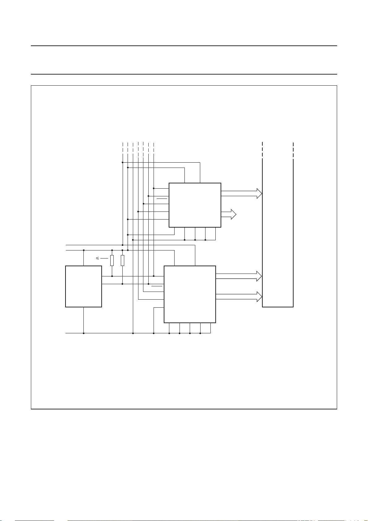
cascade. Such an arrangement is cost-effective in large
LCD applications since the backplane outputs of only one
device need to be through-plated to the backplane
electrodes of the display. The other PCF8576s of the
cascade contribute additional segment outputs but their
backplane outputs are left open-circuit (see Fig.18).
The SYNC line is provided to maintain the correct
synchronization between all cascaded PCF8576s. This
synchronization is guaranteed after the Power-on reset.
The only time that SYNC is likely to be needed is if
synchronization is accidentally lost (e.g. by noise in
adverse electrical environments; or by the definition of a
multiplex mode when PCF8576s with differing SA0 levels
are cascaded). SYNC is organized as an input/output pin;
the output selection being realized as an open-drain driver
with an internal pull-up resistor. A PCF8576 asserts the
SYNC line at the onset of its last active backplane signal
and monitors the SYNC line at all other times. Should
synchronization in the cascade be lost, it will be restored
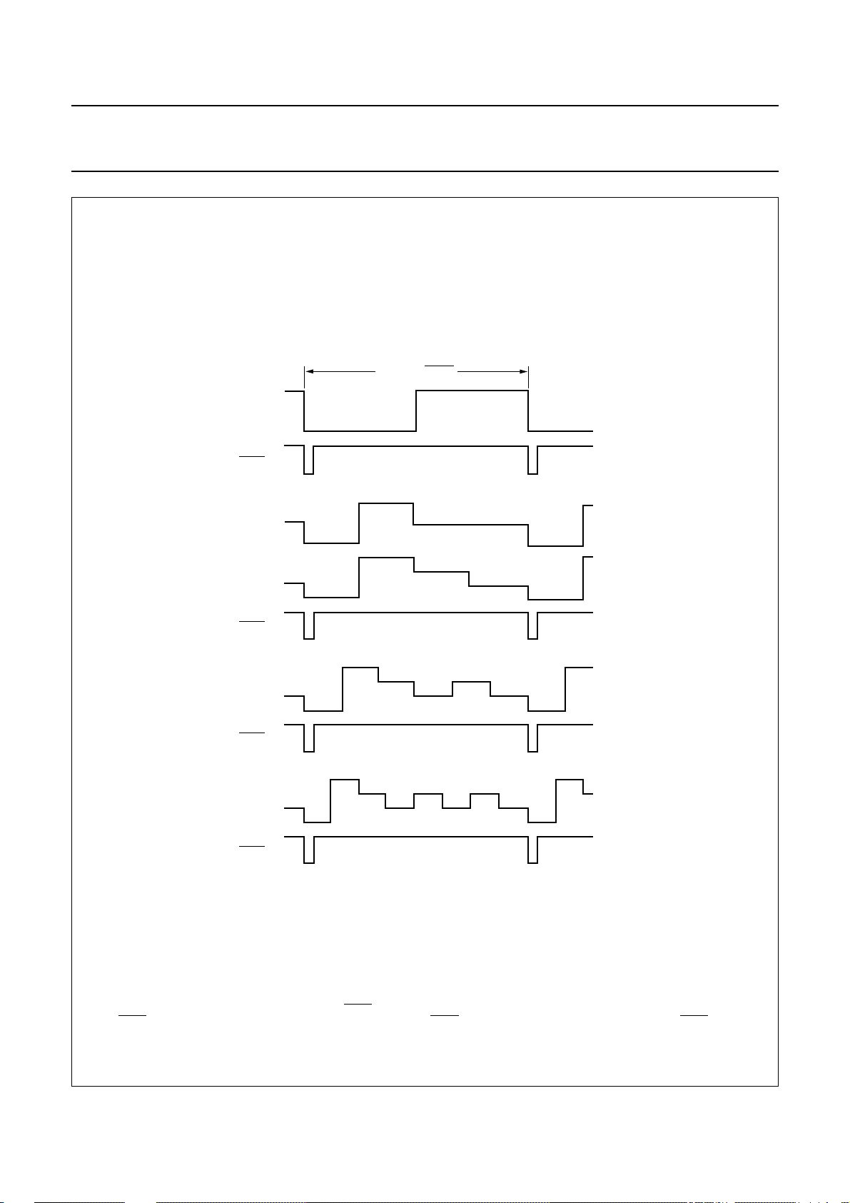
by the first PCF8576 to assert SYNC. The timing
relationship between the backplane waveforms and the
SYNC signal for the various drive modes of the PCF8576
are shown in Fig.19.
2001 Oct 02 24
For single plane wiring of packaged PCF8576s and
chip-on-glass cascading, see Chapter 12.
Page 25
Philips Semiconductors Product specification
Universal LCD driver for low multiplex rates PCF8576
handbook, full pagewidth
V
DDVLCD
512
1
2
3
PCF8576
4
6
7 8 9 10 11
A0 A1 A2 SA0 V
17 to 56
13, 15
14, 16
40 segment drives
LCD PANEL
(up to 2560
elements)
BP0 to BP3
(open-circuit)
SS
V
SDA
SCL
SYNC
CLK
OSC
LCD
V
DD
HOST
MICRO-
PROCESSOR/
MICRO-
CONTROLLER
V
SS
t
r
R
2C
B
SDA
SCL
SYNC
CLK
OSC
V
512
1
2
3
4
6
78
A0 A1 A2SSSA0 V
DD
PCF8576
91011
V
LCD
17 to 56
13, 15
14, 16
40 segment drives
4 backplanes
BP0 to BP3
MBK280
Fig.18 Cascaded PCF8576 configuration.
2001 Oct 02 25
Page 26
Philips Semiconductors Product specification
Universal LCD driver for low multiplex rates PCF8576
handbook, full pagewidth
BP0
SYNC
BP1
(1/2 bias)
BP1
(1/3 bias)
SYNC
BP2
SYNC
T=
framefframe
(a) static drive mode.
(b) 1 : 2 multiplex drive mode.
(c) 1 : 3 multiplex drive mode.
1
BP3
SYNC
(d) 1 : 4 multiplex drive mode.
Excessive capacitive coupling between SCL or CLK and SYNC may cause erroneous synchronization. If this proves to be a problem, the capacitance
SYNC lineshouldbe increased (e.g. by anexternal capacitor between SYNC and VDD). Degradationofthe positive edge of theSYNC pulse may
of the
be countered by an external pull-up resistor.
MBE535
Fig.19 Synchronization of the cascade for the various PCF8576 drive modes.
2001 Oct 02 26
Page 27

Philips Semiconductors Product specification
Universal LCD driver for low multiplex rates PCF8576
8 LIMITING VALUES
In accordance with the Absolute Maximum Rating System (IEC 60134).
SYMBOL PARAMETER MIN. MAX. UNIT
V
DD
V
LCD
V
I
V
O
I
I
I
O
I
, ISS, I
DD
P
tot
P
O
T
stg
9 HANDLING
supply voltage −0.5 +11.0 V
LCD supply voltage VDD− 11.0 V
DD
input voltage SDA, SCL, CLK, SYNC, SA0, OSC, A0 to A2 VSS− 0.5 VDD+ 0.5 V
output voltage S0 to S39, BP0 to BP3 V
− 0.5 VDD+ 0.5 V
LCD
DC input current − 20 mA
DC output current − 25 mA
LCDVDD
, VSS or V
current − 50 mA
LCD
total power dissipation − 400 mW
power dissipation per output − 100 mW
storage temperature −65 +150 °C
V
Inputs and outputs are protected against electrostatic discharge in normal handling. However, to be totally safe, it is
desirable to take normal precautions appropriate to handling MOS devices (see
“Handling MOS Devices”
).
2001 Oct 02 27
Page 28
Philips Semiconductors Product specification
Universal LCD driver for low multiplex rates PCF8576
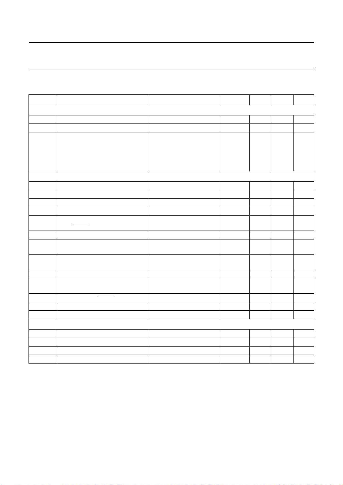
10 DC CHARACTERISTICS
VDD= 2 to 9 V; VSS=0V; V
LCD=VDD
SYMBOL PARAMETER CONDITIONS MIN. TYP. MAX. UNIT
Supplies
V
DD
V
LCD
I
DD
supply voltage 2 − 9V
LCD supply voltage note 1 VDD− 9 − VDD− 2V
supply current note 2
normal mode f
power-saving mode f
Logic
V
IL
V
IH
V
OL
V
OH
I
OL1
LOW-level input voltage V
HIGH-level input voltage 0.7V
LOW-level output voltage IOL=0mA −−0.05 V
HIGH-level output voltage IOH=0mA VDD− 0.05 −− V
LOW-level output current
CLK, SYNC
I
OH1
I
OL2
HIGH-level output current CLK VOH=4V; VDD=5V 1 −− mA
LOW-level output current
SDA and SCL
I
L1
leakage current SA0, A0 to A2,
CLK, SDA and SCL
I
L2
I
pd
leakage current OSC VI=V
A0, A1, A2 and OSC pull-down
current
R
V
C
SYNC
POR
I
pull-up resistor (SYNC) 20 50 150 kΩ
Power-on reset voltage level note 3 − 1.0 1.6 V
input capacitance note 4 −−7pF
LCD outputs
V
BP
V
S
R
BP
R
S
DC voltage component BP0 to BP3 CBP=35nF − 20 − mV
DC voltage component S0 to S39 CS=5nF − 20 − mV
output resistance BP0 to BP3 note 5; V
output resistance S0 to S39 note 5; V
− 2VtoVDD− 9 V; T
= 200 kHz −−180 µA
clk
= 35 kHz; VDD= 3.5 V;
clk
V
= 0 V; A0, A1 and A2
LCD
connected to V
VOL=1V; VDD=5V 1 −− mA
VOL= 0.4 V; VDD=5V 3 −− mA
VI=VDD or V
DD
VI=1V; VDD= 5 V 20 50 150 µA
= −40 to +85 °C; unless otherwise specified.
amb
−−60 µA
SS
− 0.3V
− V
SS
SS
DD
−−1µA
−−1µA
LCD=VDD
LCD=VDD
− 5V −−5kΩ
− 5V −−7.5 kΩ
DD
DD
V
V
Notes
1. V
≤ VDD− 3 V for1⁄3bias.
LCD
2. LCD outputs are open-circuit; inputs at VSS or VDD; external clock with 50% duty factor; I2C-bus inactive.
3. Resets all logic when VDD<V
POR
.
4. Periodically sampled, not 100% tested.
5. Outputs measured one at a time.
2001 Oct 02 28
Page 29
Philips Semiconductors Product specification
Universal LCD driver for low multiplex rates PCF8576
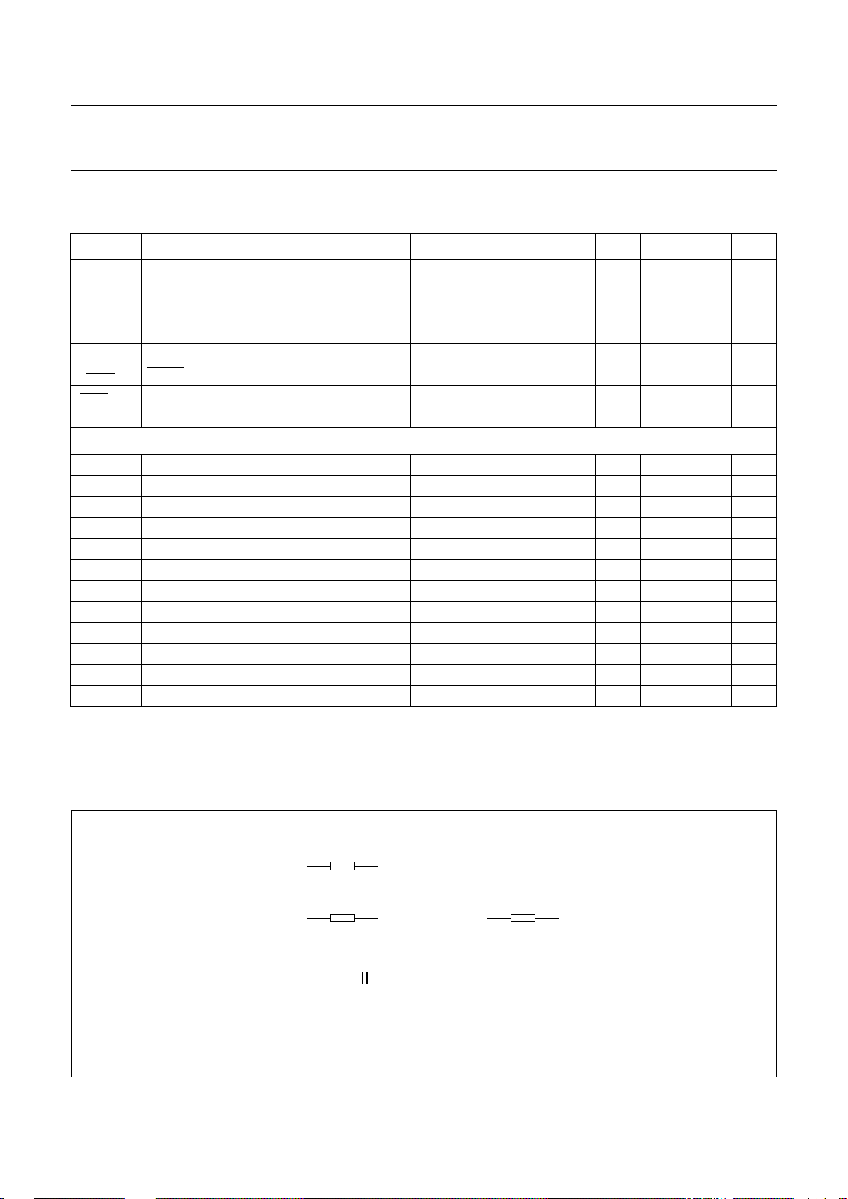
11 AC CHARACTERISTICS
VDD= 2 to 9 V; VSS=0V; V
LCD=VDD
SYMBOL PARAMETER CONDITIONS MIN. TYP. MAX. UNIT
f
clk
oscillator frequency on pin CLK
normal mode V
power-saving mode V
t
clkH
t
clkL
t
PSYNC
t
SYNCL
t
PLCD
Timing characteristics: I
t
SW
t
BUF
t
HD;STA
t
SU;STA
t
LOW
t
HIGH
t
r
t
f
C
B
t
SU;DAT
t
HD;DAT
t
SU;STO
CLK HIGH time see Fig.21 1 −−µs
CLK LOW time 1 −−µs
SYNC propagation delay time −−400 ns
SYNC LOW time 1 −−µs
driver delays with test loads V
2
C-bus; note 2; see Fig.22
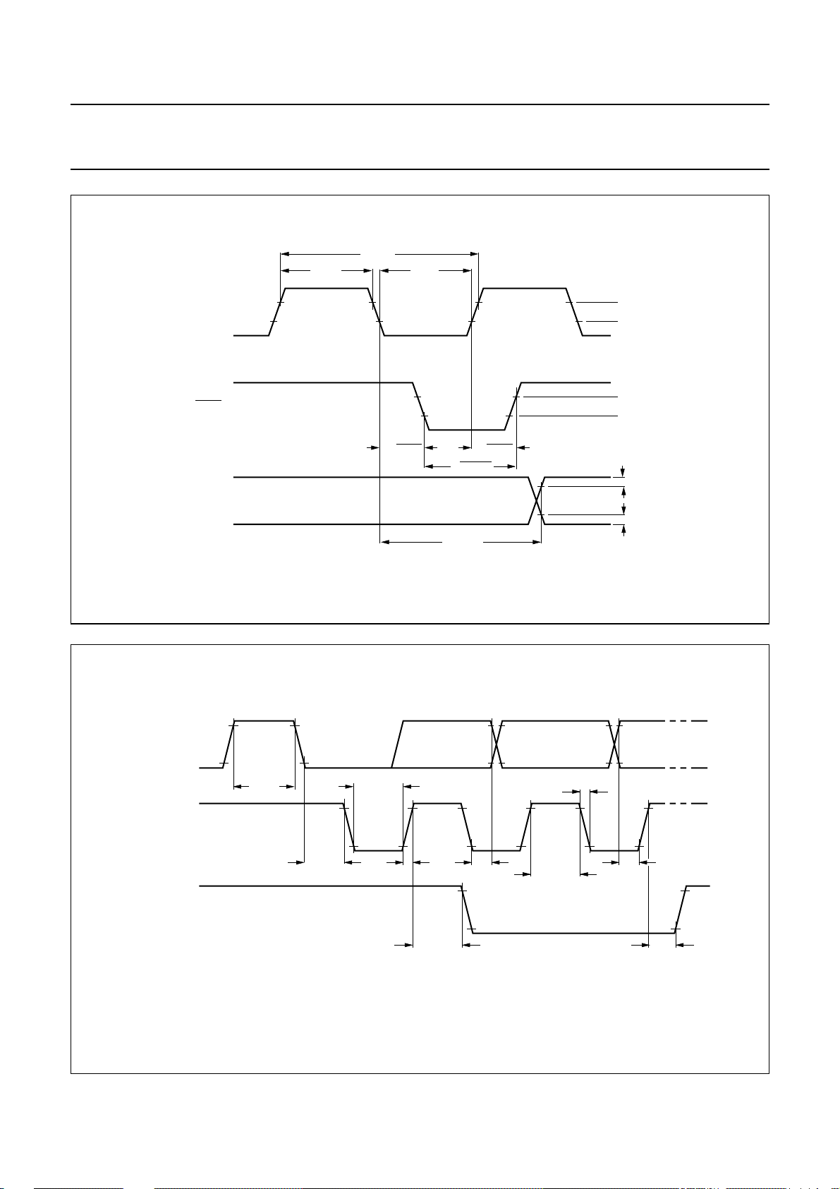
tolerable spike width on bus −−100 ns
bus free time 4.7 −−µs
START condition hold time 4.0 −−µs
set-up time for a repeated START condition 4.7 −−µs
SCL LOW time 4.7 −−µs
SCL HIGH time 4.0 −−µs
SCL and SDA rise time −−1µs
SCL and SDA fall time −−0.3 µs
capacitive bus line load −−400 pF
data set-up time 250 −−ns
data hold time 0 −−ns
set-up time for STOP condition 4.0 −−µs
− 2VtoVDD− 9 V; T
= −40 to +85 °C; unless otherwise specified.
amb
= 5 V; note 1 125 200 288 kHz
DD
= 3.5 V 21 31 48 kHz
DD
LCD=VDD
− 5 V; see Fig.20 −−30 µs
Notes
1. At f
< 125 kHz, I2C-bus maximum transmission speed is derated.
clk
2. All timing values are valid within the operating supply voltage and ambient temperature range and are referenced to
VIL and VIH with an input voltage swing of VSSto VDD.
SYNC
CLK
BP0 to BP3, and
S0 to S39
Ω6.8
V
(2%)
DD
Ω3.3 k Ω1.5 k
0.5V
DD
1 nF
V
DD
SDA,
SCL
V
(2%)(2%)
DD
MBE544
Fig.20 Test loads.
2001 Oct 02 29
Page 30
Philips Semiconductors Product specification
Universal LCD driver for low multiplex rates PCF8576
handbook, full pagewidth
CLK
SYNC
BP0 to BP3,
and S0 to S39
1/ f
t
clkH
clk
t
PSYNC
t
clkL
t
t
PLCD
t
PSYNC
SYNCL
Fig.21 Driver timing waveforms.
MBE545
0.7V
DD
0.3V
DD
0.7V
DD
0.3V
DD
0.5 V
(VDD = 5 V)
0.5 V
handbook, full pagewidth
SDA
SCL
SDA
MGA728
t
BUF
t
HD;STA
t
LOW
t
r
Fig.22 I2C-bus timing waveforms.
2001 Oct 02 30
t
SU;STA
t
HD;DAT
t
HIGH
t
f
t
SU;DAT
t
SU;STO
Page 31
Philips Semiconductors Product specification
Universal LCD driver for low multiplex rates PCF8576
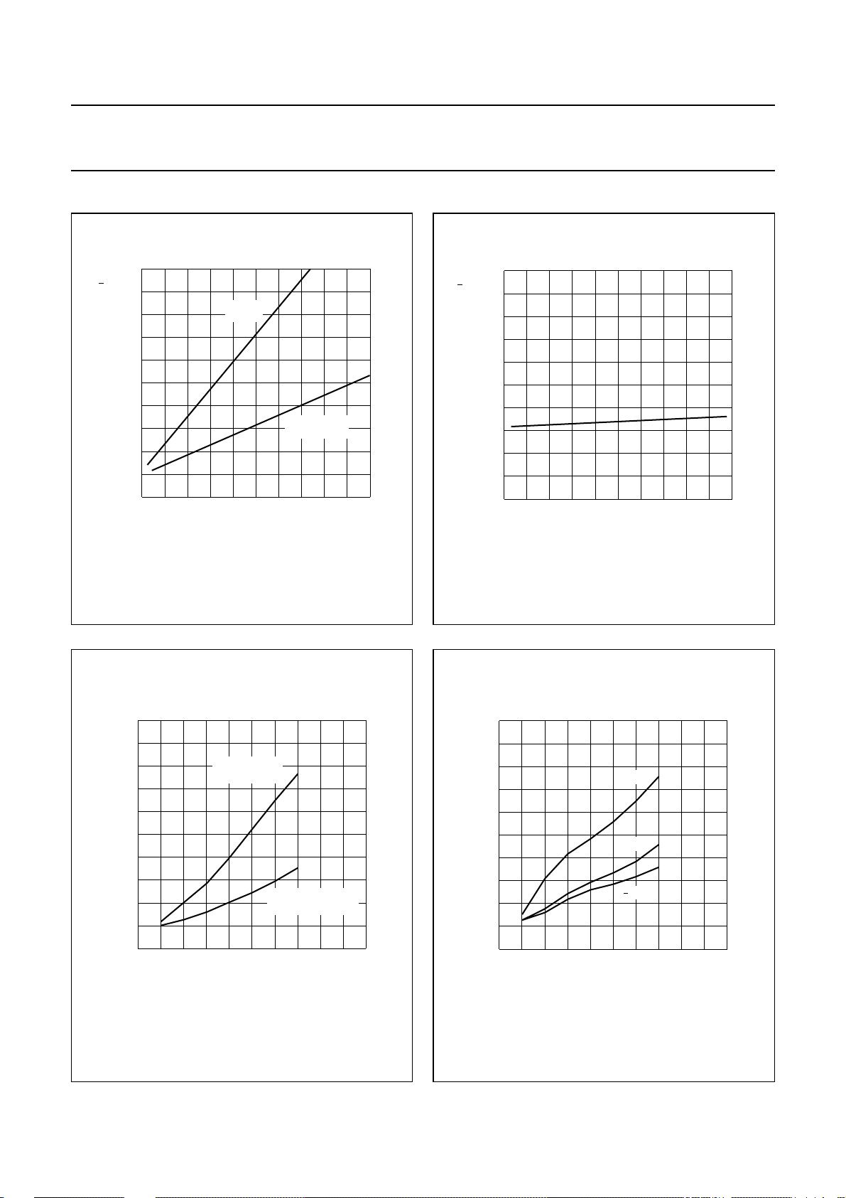
11.1 Typical supply current characteristics
50
I
SS
(µA)
40
30
20
10
0
VDD= 5 V; V
MBE530
normal
mode
power-saving
mode
=25°C.
100
f (Hz)
frame
frame
.
0 200
= 0 V; T
LCD
amb
Fig.23 −ISS as a function of f
50
I
LCD
(µA)
40
30
20
10
0
VDD= 5 V; V
MBE529
0 200
= 0 V; T
LCD
Fig.24 −I
amb
LCD
100
=25°C.
f (Hz)
frame
as a function of f
frame
.
50
handbook, halfpage
I
SS
(µA)
40
30
20
10
0
010
V
= 0 V; external clock; T
LCD
normal mode
f = 200 kHz
clk
5
=25°C.
amb
power-saving mode
MBE528 - 1
f = 35 kHz
clk
V (V)
DD
Fig.25 ISS as a function of VDD.
2001 Oct 02 31
50
handbook, halfpage
I
LCD
(µA)
40
30
20
10
0
010
V
= 0 V; external clock; f
LCD
Fig.26 I
o
85 C
o
25 C
o
40 C
5
= nominal frequency.
clk
as a function of VDD.
LCD
V (V)
DD
MBE527 - 1
Page 32
Philips Semiconductors Product specification
Universal LCD driver for low multiplex rates PCF8576
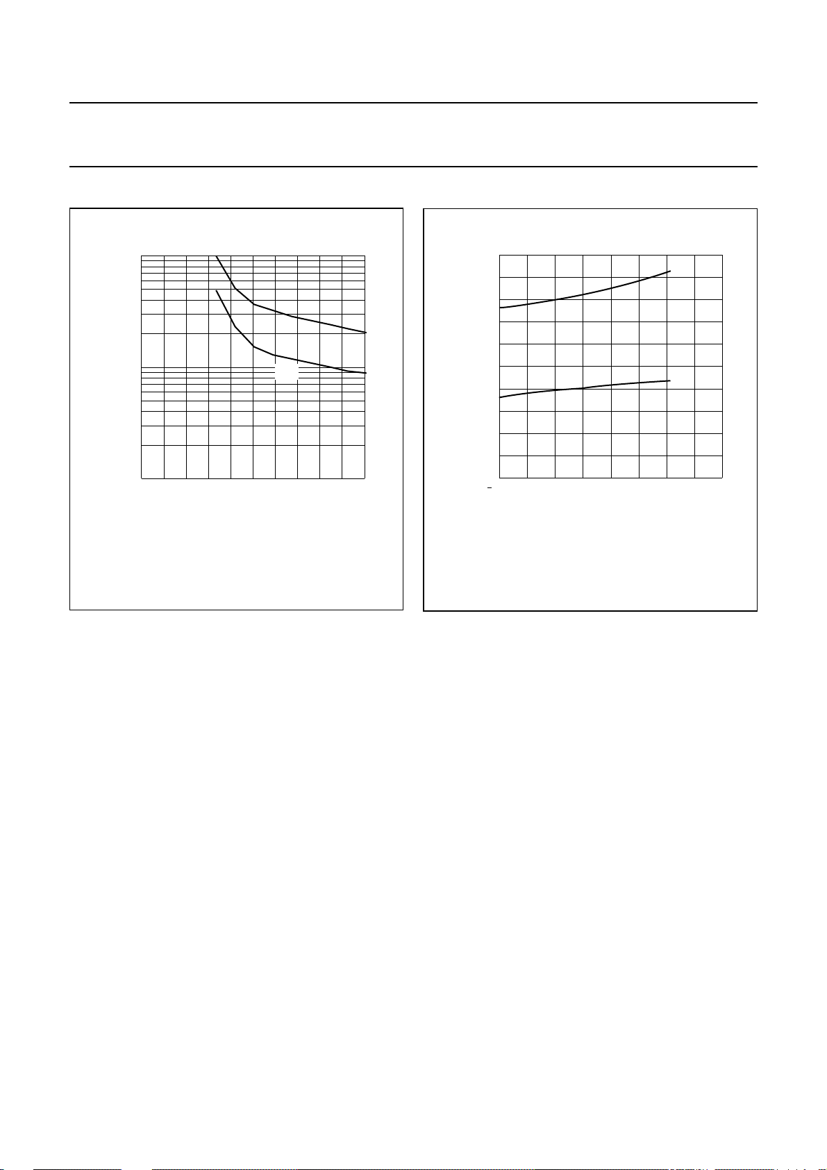
11.2 Typical characteristics of LCD outputs
10
handbook, halfpage
R
O(max)
(kΩ)
1
-1
10
V
= 0 V; T
LCD
amb
Fig.27 R
=25°C.
O(max)
MBE532 - 1
R
S
R
BP
3
V (V)
DD
as a function of VDD.
2.5
R
O(max)
(kΩ)
2.0
1.5
1.0
0.5
0
60
VDD= 5 V; V
40 0 40 120
=0V.
LCD
Fig.28 R
as a function of T
O(max)
MBE526
R
S
R
BP
80
o
( C)
T
amb
.
amb
2001 Oct 02 32
Page 33
This text is here in white to force landscape pages to be rotated correctly when browsing through the pdf in the Acrobat reader.This text is here in
a
_white to force landscape pages to be rotated correctly when browsing through the pdf in the Acrobat reader.This text is here inThis text is here in
white to force landscape pages to be rotated correctly when browsing through the pdf in the Acrobat reader. white to force landscape pages to be ...
2001 Oct 02 33
ndbook, full pagewidth
SDA
SCL
SYNC
CLK
V
DD
V
SS
V
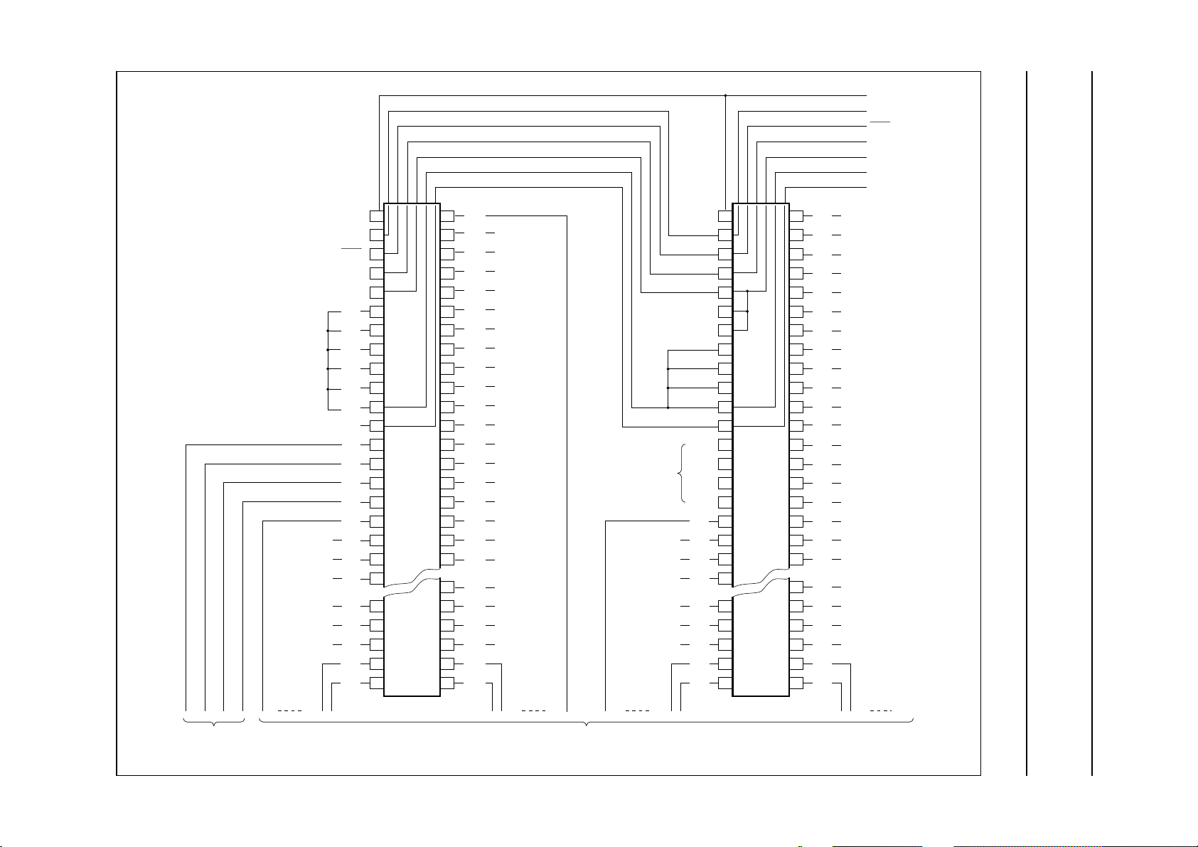
LCD
12 APPLICATION INFORMATION
Philips Semiconductors Product specification
Universal LCD driver for low multiplex rates PCF8576
SDA
SCL
SYNC
CLK
V
DD
OSC
A0
A1
A2
SA0
V
SS
V
LCD
BP0
BP2
BP1
BP3
S0
S1
S2
S3
S7
S8
S9
S10
S11
1
2
3
4
5
6
7
8
9
10
11
12
13
14
15
16
17
18
19
20
24
25
26
27
28
PCF8576T
56
S39
55
S38
54
S37
53
S36
52
S35
51
S34
50
S33
49
S32
48
S31
47
S30
46
S29
45
S28
44
S27
43
S26
42
S25
41
S24
40
S23
39
S22
38
S21
S17
34
S16
33
32
S15
31
S14
30
S13
29
S12
open
BP0
BP2
BP1
BP3
S40
S41
S42
S43
S47
S48
S49
S50
S51
1
2
3
4
5
6
7
8
9
10
11
12
13
14
15
16
17
18
19
20
24
25
26
27
28
PCF8576T
56
S79
55
S78
54
S77
53
S76
52
S75
51
S74
50
S73
49
S72
48
S71
47
S70
46
S69
45
S68
44
S67
43
S66
42
S65
41
S64
40
S63
39
S62
38
S61
S57
34
S56
33
32
S55
31
S54
30
S53
29
S52
S10 S11S0 S79
backplanes segments
Fig.29 Single plane wiring of packaged PCF8576Ts.
S50S39 S40S13S12
S51 S52 S53
MBK281
Page 34
Philips Semiconductors Product specification
Universal LCD driver for low multiplex rates PCF8576
12.1 Chip-on-glass cascadability in single plane
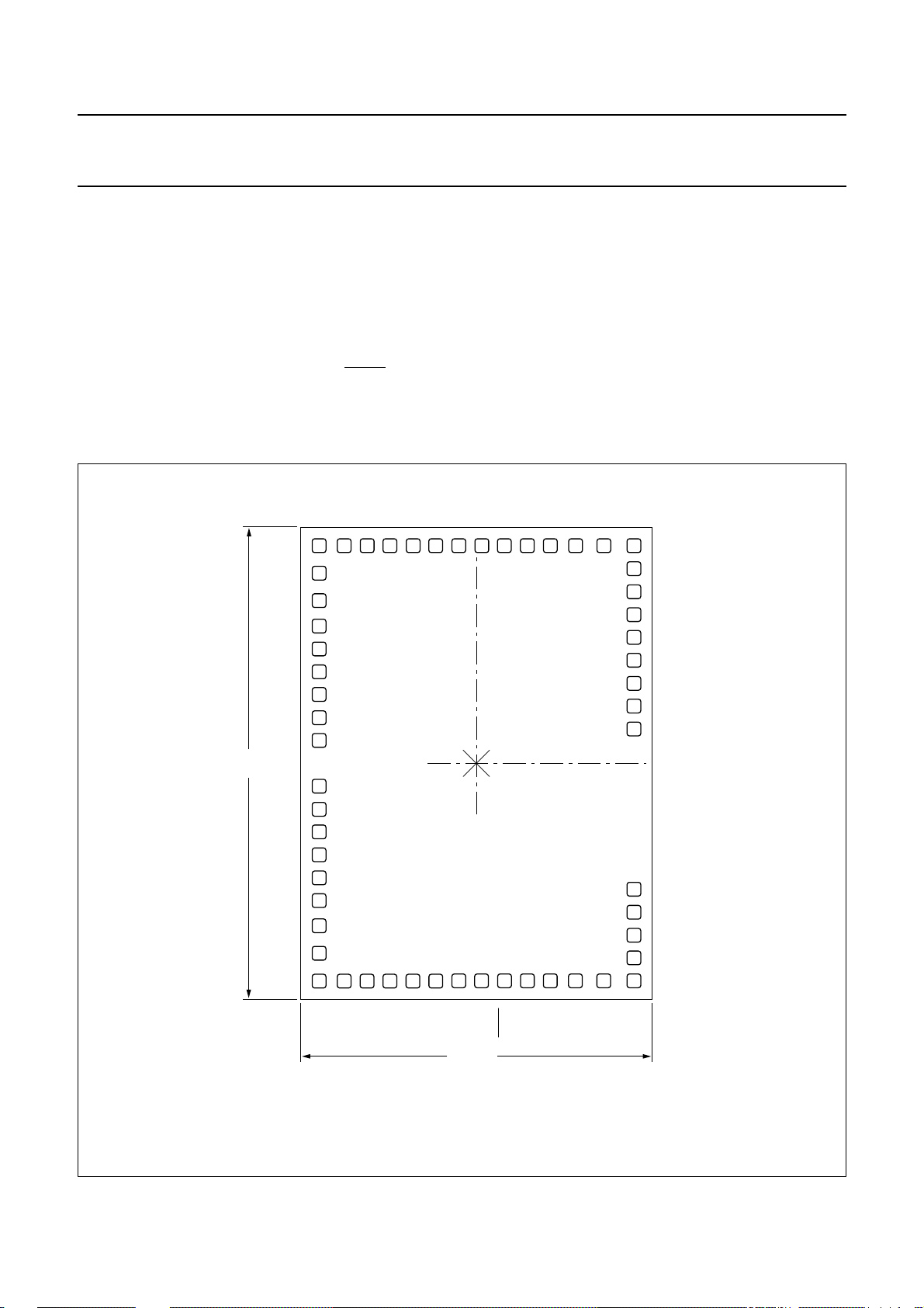
In chip-on-glass technology, where driver devices are
bonded directly onto glass of the LCD, it is important that
the devices may be cascaded without the crossing of
conductors, but the paths of conductors can be continued
on the glass under the chip. All of this is facilitated by the
PCF8576 bonding pad layout (see Fig.30). Pads needing
businterconnection between all PCF8576s of the cascade
are VDD, VSS, V
, CLK, SCL, SDA and SYNC. These
LCD
lines may be led to the corresponding pads of the next
PCF8576 through the wide opening between V
LCD
pad
13 BONDING PAD INFORMATION
handbook, full pagewidth
S18
S19
S20
S21
S22
S23
S24
S25
4.12
mm
S26
S27
S28
S29
S30
S31
S32
S33
S17
S16
S15
35
36
37
38
39
40
41
42
43
44
45
46
47
48
49
50
51
52 53 54 55 56
S14
S13
x
andthebackplaneoutputpads.Theonlybusline that does
not require a second opening to lead through to the next
PCF8576 is V
of V
adjacent to VSS allows the two supplies to be
LCD
, being the cascade centre. The placing
LCD
connected together.
Whenan external clocking source is to beused, OSC of all
devices should be connected to VDD. The pads OSC,
A0, A1, A2 and SA0 have been placed between
VSSand VDD to facilitate wiring of oscillator, hardware
subaddress and slave address.
S12
S11
S10S9S8
0
0
y
PCF8576
1 2 3 4 5 6 7
S7
S6
cascade
centre
S5
S4
2122232425262728293031323334
20
S3
19
S2
18
S1
17
S0
16
BP3
15
BP1
14
BP2
13
BP0
V
12
LCD
V
11
SS
10
SA0
9
A2
8
S39
S38
S37
S36
S35
S34
3.07 mm
Bonding pad dimensions: 120 × 120 µm.
Gold bump dimensions: 94 × 94 × 25 µm.
Fig.30 Bonding pad locations.
2001 Oct 02 34
SDA
SCL
SYNC
CLK
V
DD
OSC
A0
MBK282
A1
Page 35
Philips Semiconductors Product specification
Universal LCD driver for low multiplex rates PCF8576
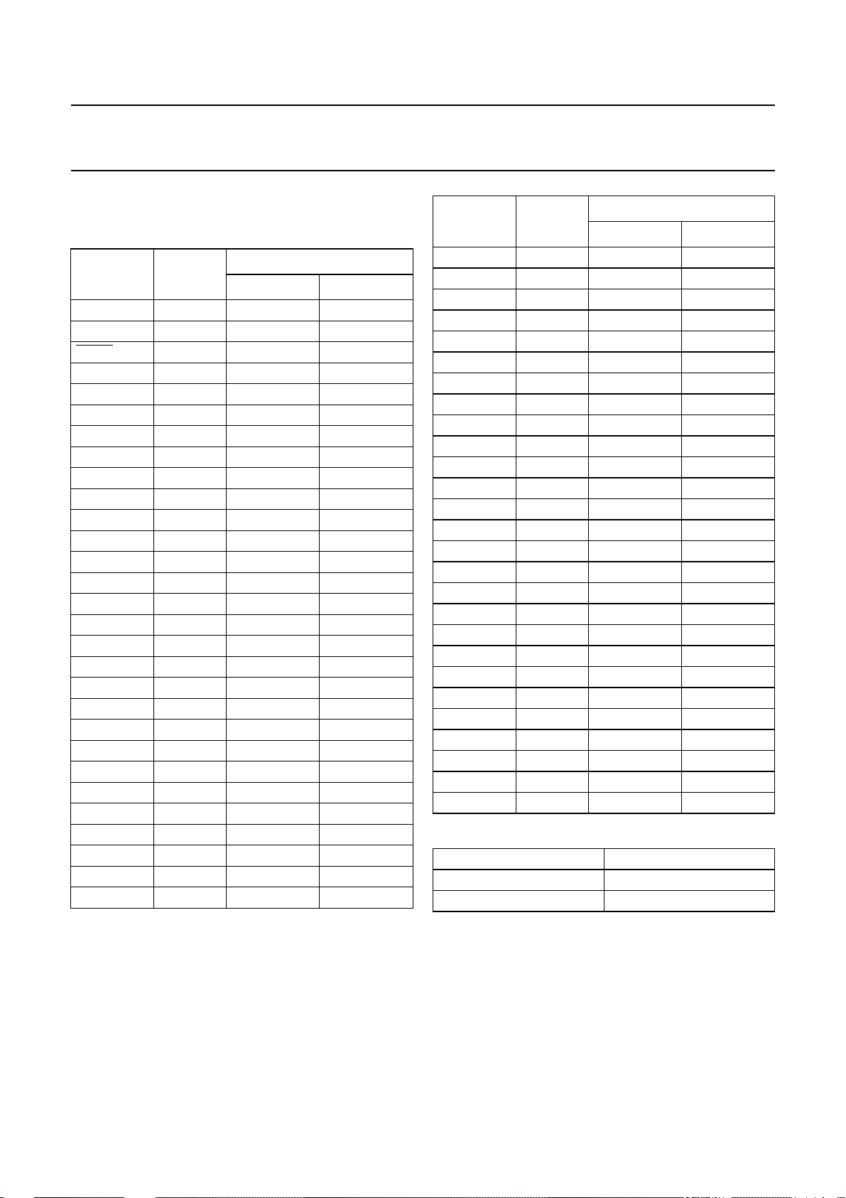
Table 15 Bonding pad locations (dimensions in µm)
All x and y coordinates are referenced to centre of chip
(see Fig.30).
COORDINATES
SYMBOL PAD
xy
SDA 1 −155 −1900
SCL 2 45 −1900
SYNC 3 245 −1900
CLK 4 445 −1900
V
DD
5 645 −1900
OSC 6 865 −1900
A0 7 1105 −1900
A1 8 1375 −1900
A2 9 1375 −1700
SA0 10 1375 −1500
V
V
SS
LCD
11 1375 −1300
12 1375 −1100
BP0 13 1375 300
BP2 14 1375 500
BP1 15 1375 700
BP3 16 1375 900
S0 17 1375 1100
S1 18 1375 1300
S2 19 1375 1500
S3 20 1375 1700
S4 21 1375 1900
S5 22 1105 1900
S6 23 865 1900
S7 24 645 1900
S8 25 445 1900
S9 26 245 1900
S10 27 45 1900
S11 28 −155 1900
S12 29 −355 1900
SYMBOL PAD
COORDINATES
xy
S13 30 −555 1900
S14 31 −755 1900
S15 32 −955 1900
S16 33 −1155 1900
S17 34 −1375 1900
S18 35 −1375 1660
S19 36 −1375 1420
S20 37 −1375 1200
S21 38 −1375 1000
S22 39 −1375 800
S23 40 −1375 600
S24 41 −1375 400
S25 42 −1375 200
S26 43 −1375 −200
S27 44 −1375 −400
S28 45 −1375 −600
S29 46 −1375 −800
S30 47 −1375 −1000
S31 48 −1375 −1200
S32 49 −1375 −1420
S33 50 −1375 −1660
S34 51 −1375 −1900
S35 52 −1155 −1900
S36 53 −955 −1900
S37 54 −755 −1900
S38 55 −555 −1900
S39 56 −355 −900
Table 16 Bonding pad dimensions
Pad pitch 200 µm
Pad size, aluminium 120 × 120 µm
Gold bump dimensions 94 × 94 × 25 µm
2001 Oct 02 35
Page 36
Philips Semiconductors Product specification
Universal LCD driver for low multiplex rates PCF8576
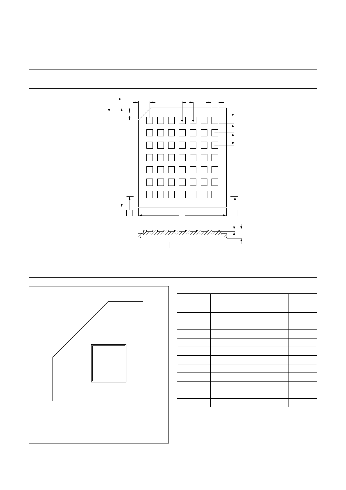
14 TRAY INFORMATION: PCF8576U
handbook, full pagewidth
For dimensions see Table 18.
x
y
F
G
H
1,1 x,12,1
1,2
1,y
A
A
E
SECTION A-A
C
D
B
x,y
A
M
J
MGU431
handbook, halfpage
PC8576U
MGU432
The orientation of the IC in a pocket is indicated by the
position ofthe IC type name onthe die surface withrespect to
the chamfer on the upper left corner of the tray.
Fig.32 Tray alignment.
Fig.31 Tray details.
Table 17 Tray dimensions (see Fig.33)
SYMBOL DESCRIPTION VALUE
A pocket pitch; x direction 6.32 mm
B pocket pitch; y direction 6.32 mm
C pocket width; x direction 4.55 mm
D pocket width; y direction 4.55 mm
E tray width; x direction 50.67 mm
F tray width; y direction 50.67 mm
G cut corner to pocket 1,1 centre 6.32mm
H cut corner to pocket 1,1 centre 6.32mm
J tray thickness 3.94 mm
M pocket depth 0.61 mm
x number of pockets; x direction 7
y number of pockets; y direction 7
2001 Oct 02 36
Page 37
Philips Semiconductors Product specification
Universal LCD driver for low multiplex rates PCF8576
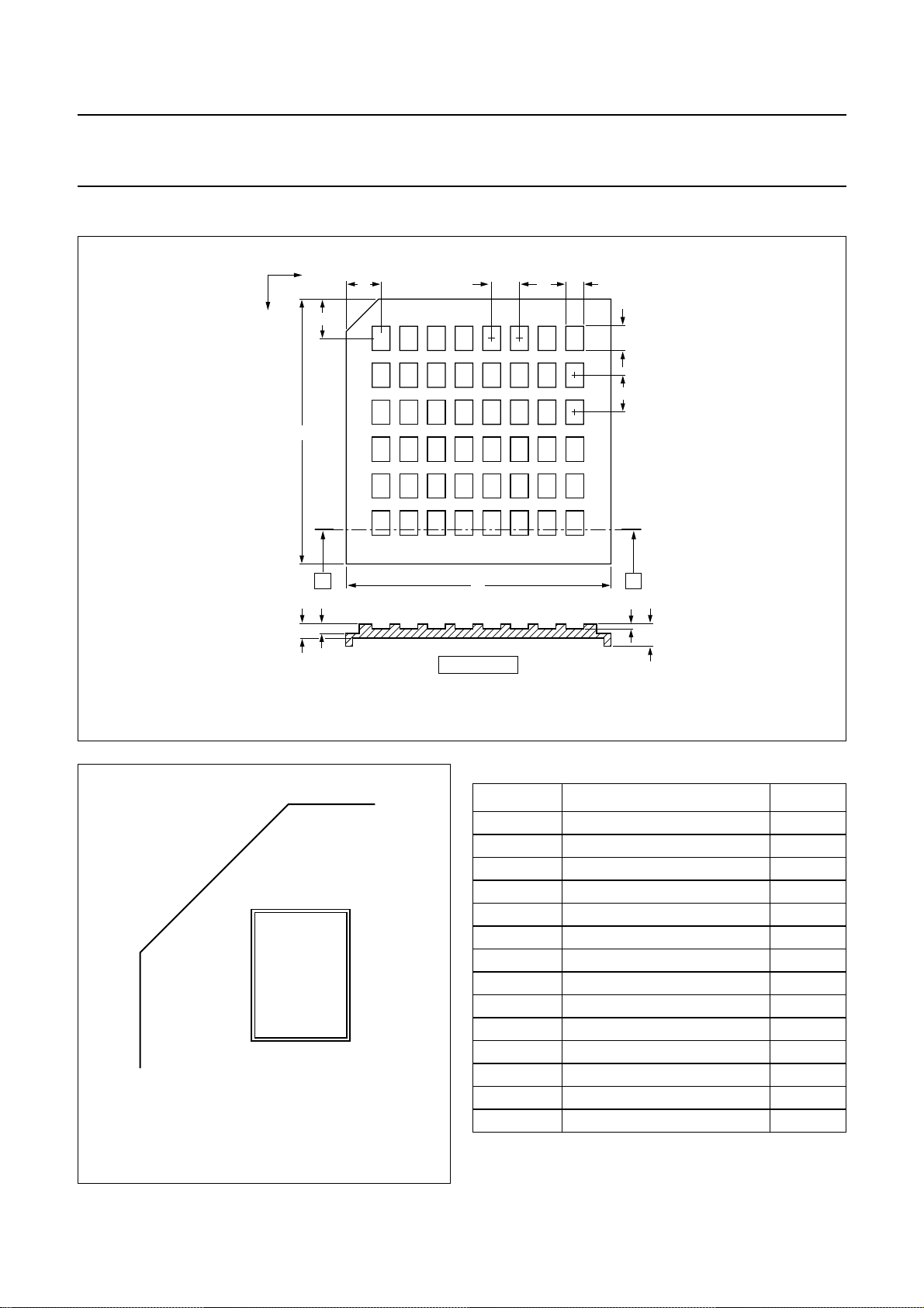
15 TRAY INFORMATION: PCF8576U/2
handbook, full pagewidth
For dimensions see Table 17.
x
y
F
L
G
H
1,1 x,12,1
1,2
1,y
A
K
SECTION A-A
A
E
C
D
B
x,y
A
M
J
MGW014
Fig.33 Tray details.
handbook, halfpage
PCF8576U/2
MGW015
The orientation of the IC in a pocket is indicated by the
position ofthe IC type name onthe die surface withrespect to
the chamfer on the upper left corner of the tray.
Fig.34 Tray alignment.
2001 Oct 02 37
Table 18 Tray dimensions (see Fig.31)
SYMBOL DESCRIPTION VALUE
A pocket pitch; x direction 5.33 mm
B pocket pitch; y direction 7.11 mm
C pocket width; x direction 3.43 mm
D pocket width; y direction 4.67 mm
E tray width; x direction 50.67 mm
F tray width; y direction 50.67 mm
G cut corner to pocket 1,1 centre 6.67mm
H cut corner to pocket 1,1 centre 7.56mm
J tray thickness 3.94 mm
K tray cross section 1.76mm
L tray cross section 2.46mm
M pocket depth 0.89 mm
x number of pockets; x direction 8
y number of pockets; y direction 6
Page 38
Philips Semiconductors Product specification
Universal LCD driver for low multiplex rates PCF8576
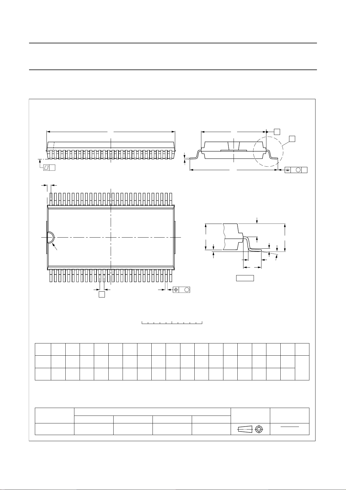
16 PACKAGE OUTLINES
VSO56: plastic very small outline package; 56 leads
D
y
Z
56
pin 1 index
SOT190-1
E
c
H
E
29
Q
A
2
A
1
L
p
L
(A )
A
X
v M
A
A
3
θ
281
w M
b
e
0 5 10 mm
DIMENSIONS (inch dimensions are derived from the original mm dimensions)
mm
OUTLINE
VERSION
SOT190-1
A
max.
3.3
0.13
0.3
0.1
0.012
0.004
b
3
p
3.0
2.8
0.12
0.11
IEC JEDEC EIAJ
0.25
0.01
0.42
0.30
0.017
0.012
0.22
0.14
0.0087
0.0055
UNIT A1A2A
inches
Note
1. Plastic or metal protrusions of 0.3 mm maximum per side are not included.
2. Plastic interlead protrusions of 0.25 mm maximum per side are not included.
(1)E(2)
cD
21.65
21.35
0.85
0.84
REFERENCES
p
scale
eHELLpQZywv θ
11.1
0.75
11.0
0.44
0.0295
0.43
15.8
15.2
0.62
0.60
2.25
0.089
1.6
1.4
0.063
0.055
detail X
1.45
0.2
1.30
0.057
0.008 0.004
0.051
EUROPEAN
PROJECTION
0.1 0.1
0.004
(1)
0.90
0.55
0.035
0.022
ISSUE DATE
96-04-02
97-08-11
o
7
o
0
2001 Oct 02 38
Page 39

Philips Semiconductors Product specification
Universal LCD driver for low multiplex rates PCF8576
17 SOLDERING
17.1 Introduction to soldering surface mount packages
Thistextgivesaverybriefinsighttoacomplextechnology.
A more in-depth account of soldering ICs can be found in
our
“Data Handbook IC26; Integrated Circuit Packages”
(document order number 9398 652 90011).
There is no soldering method that is ideal for all surface
mount IC packages. Wave soldering can still be used for
certainsurfacemountICs,butitisnotsuitableforfinepitch
SMDs. In these situations reflow soldering is
recommended.
17.2 Reflow soldering
Reflow soldering requires solder paste (a suspension of
fine solder particles, flux and binding agent) to be applied
totheprinted-circuit board by screen printing, stencilling or
pressure-syringe dispensing before package placement.
Several methods exist for reflowing; for example,
convection or convection/infrared heating in a conveyor
type oven. Throughput times (preheating, soldering and
cooling) vary between 100 and 200 seconds depending
on heating method.
Typical reflow peak temperatures range from
215 to 250 °C. The top-surface temperature of the
packages should preferable be kept below 220 °C for
thick/large packages, and below 235 °C for small/thin
packages.
17.3 Wave soldering
Conventional single wave soldering is not recommended
forsurfacemountdevices(SMDs)orprinted-circuitboards
with a high component density, as solder bridging and
non-wetting can present major problems.
To overcome these problems the double-wave soldering
method was specifically developed.
If wave soldering is used the following conditions must be
observed for optimal results:
• Use a double-wave soldering method comprising a
turbulent wave with high upward pressure followed by a
smooth laminar wave.
• For packages with leads on two sides and a pitch (e):
– larger than or equal to 1.27 mm, the footprint
longitudinal axis is preferred to be parallel to the
transport direction of the printed-circuit board;
– smaller than 1.27 mm, the footprint longitudinal axis
must be parallel to the transport direction of the
printed-circuit board.
The footprint must incorporate solder thieves at the
downstream end.
• Forpackageswithleadsonfoursides,thefootprintmust
be placed at a 45° angle to the transport direction of the
printed-circuit board. The footprint must incorporate
solder thieves downstream and at the side corners.
During placement and before soldering, the package must
be fixed with a droplet of adhesive. The adhesive can be
applied by screen printing, pin transfer or syringe
dispensing. The package can be soldered after the
adhesive is cured.
Typical dwell time is 4 seconds at 250 °C.
A mildly-activated flux will eliminate the need for removal
of corrosive residues in most applications.
17.4 Manual soldering
Fix the component by first soldering two
diagonally-opposite end leads. Use a low voltage (24 V or
less) soldering iron applied to the flat part of the lead.
Contact time must be limited to 10 seconds at up to
300 °C.
When using a dedicated tool, all other leads can be
soldered in one operation within 2 to 5 seconds between
270 and 320 °C.
2001 Oct 02 39
Page 40

Philips Semiconductors Product specification
Universal LCD driver for low multiplex rates PCF8576
17.5 Suitability of surface mount IC packages for wave and reflow soldering methods
PACKAGE
WAVE REFLOW
(1)
BGA, HBGA, LFBGA, SQFP, TFBGA not suitable suitable
SOLDERING METHOD
HBCC, HLQFP, HSQFP, HSOP, HTQFP, HTSSOP, HVQFN, SMS not suitable
(3)
PLCC
, SO, SOJ suitable suitable
LQFP, QFP, TQFP not recommended
SSOP, TSSOP, VSO not recommended
(2)
(3)(4)
(5)
suitable
suitable
suitable
Notes
1. All surface mount (SMD) packages are moisture sensitive. Depending upon the moisture content, the maximum
temperature (with respect to time) and body size of the package, there is a risk that internal or external package
cracks may occur due to vaporization of the moisture in them (the so called popcorn effect). For details, refer to the
Drypack information in the
“Data Handbook IC26; Integrated Circuit Packages; Section: Packing Methods”
.
2. These packages are not suitable for wave soldering as a solder joint between the printed-circuit board and heatsink
(at bottom version) can not be achieved, and as solder may stick to the heatsink (on top version).
3. If wave soldering is considered, then the package must be placed at a 45° angle to the solder wave direction.
The package footprint must incorporate solder thieves downstream and at the side corners.
4. Wave soldering is only suitable for LQFP, TQFP and QFP packages with a pitch (e) equal to or larger than 0.8 mm;
it is definitely not suitable for packages with a pitch (e) equal to or smaller than 0.65 mm.
5. Wave soldering is only suitable for SSOP and TSSOP packages with a pitch (e) equal to or larger than 0.65 mm; it is
definitely not suitable for packages with a pitch (e) equal to or smaller than 0.5 mm.
2001 Oct 02 40
Page 41

Philips Semiconductors Product specification
Universal LCD driver for low multiplex rates PCF8576
18 DATA SHEET STATUS
PRODUCT
DATA SHEET STATUS
Objective specification Development This data sheet contains data from the objective specification for product
Preliminary specification Qualification This data sheet contains data from the preliminary specification.
Product specification Production This data sheet contains data from the product specification. Philips
(1)
STATUS
(2)
development. Philips Semiconductors reserves the right to change the
specification in any manner without notice.
Supplementary data will be published at a later date. Philips
Semiconductors reserves the right to change the specification without
notice, in order to improve the design and supply the best possible
product.
Semiconductors reserves the right to make changes at any time in order
to improve the design, manufacturing and supply. Changes will be
communicated according to the Customer Product/Process Change
Notification (CPCN) procedure SNW-SQ-650A.
DEFINITIONS
Notes
1. Please consult the most recently issued data sheet before initiating or completing a design.
2. The product status of the device(s) described in this data sheet may have changed since this data sheet was
published. The latest information is available on the Internet at URL http://www.semiconductors.philips.com.
19 DEFINITIONS
Short-form specification The data in a short-form
specification is extracted from a full data sheet with the
same type number and title. For detailed information see
the relevant data sheet or data handbook.
Limiting values definition Limiting values given are in
accordance with the Absolute Maximum Rating System
(IEC 60134). Stress above one or more of the limiting
values may cause permanent damage to the device.
These are stress ratings only and operation of the device
attheseoratanyotherconditionsabove those given in the
Characteristics sections of the specification is not implied.
Exposure to limiting values for extended periods may
affect device reliability.
Application information Applications that are
described herein for any of these products are for
illustrative purposes only. Philips Semiconductors make
norepresentationorwarrantythatsuchapplicationswillbe
suitable for the specified use without further testing or
modification.
20 DISCLAIMERS Life support applications These products are not
designed for use in life support appliances, devices, or
systems where malfunction of these products can
reasonably be expected to resultin personal injury. Philips
Semiconductorscustomersusingorsellingtheseproducts
for use in such applications do so at their own risk and
agree to fully indemnify Philips Semiconductors for any
damages resulting from such application.
Right to make changes Philips Semiconductors
reserves the right to make changes, without notice, in the
products, including circuits, standard cells, and/or
software, described or contained herein in order to
improve design and/or performance. Philips
Semiconductors assumes no responsibility or liability for
theuseofanyoftheseproducts,conveysnolicenceortitle
under any patent, copyright, or mask work right to these
products,andmakesno representations or warranties that
these products are free from patent, copyright, or mask
work right infringement, unless otherwise specified.
Bare die All die are tested and are guaranteed to
comply with all data sheet limits up to the point of wafer
sawing for a period of ninety (90) days from the date of
Philips' delivery. If there are data sheet limits not
guaranteed, these will be separately indicated in the data
sheet. There are no post packing tests performed on
individual die or wafer. Philips Semiconductors has no
control of third party procedures in the sawing, handling,
packing or assembly of the die. Accordingly, Philips
Semiconductors assumes no liability for device
functionality or performance of the die or systems after
third party sawing, handling, packing or assembly of the
die. It is the responsibility of the customer to test and
qualify their application in which the die is used.
2001 Oct 02 41
Page 42

Philips Semiconductors Product specification
Universal LCD driver for low multiplex rates PCF8576
21 PURCHASE OF PHILIPS I2C COMPONENTS
Purchase of Philips I
components in the I2C system provided the system conforms to the I2C specification defined by
Philips. This specification can be ordered using the code 9398 393 40011.
2
C components conveys a license under the Philips’ I2C patent to use the
2001 Oct 02 42
Page 43

Philips Semiconductors Product specification
Universal LCD driver for low multiplex rates PCF8576
NOTES
2001 Oct 02 43
Page 44

Philips Semiconductors – a w orldwide compan y
Contact information
For additional information please visit http://www.semiconductors.philips.com. Fax: +31 40 27 24825
For sales offices addresses send e-mail to: [email protected].
© Koninklijke Philips Electronics N.V. 2001
All rights are reserved. Reproduction in whole or in part is prohibited without the prior written consent of the copyright owner.
The information presented in this document does not form part of any quotation or contract, is believed to be accurate and reliable and may be changed
without notice. No liability will be accepted by the publisher for any consequence of its use. Publication thereof does not convey nor imply any license
under patent- or other industrial or intellectual property rights.
Printed in The Netherlands 403512/04/pp44 Date of release: 2001 Oct 02 Document order number: 9397 750 08044
SCA73
 Loading...