

Philips pcf85116 DATASHEETS
INTEGRATED CIRCUITS
DATA SH EET
PCF85116-3
2048 × 8-bit CMOS EEPROM with
2
I
C-bus interface
Product specification
Supersedes data of 1997 Feb 24
File under Integrated Circuits, IC12
1997 Apr 02

Philips Semiconductors Product specification
2048 × 8-bit CMOS EEPROM with I2C-bus
interface
CONTENTS
1 FEATURES
2 DESCRIPTION
2.1 Remark
3 QUICK REFERENCE DATA
4 ORDERING INFORMATION
5 DEVICE SELECTION
6 BLOCK DIAGRAM
7 PINNING
8I
8.1 Bus conditions
8.2 Data transfer
8.3 Device addressing
8.4 Write operations
8.4.1 Byte/word write
8.4.2 Page Write
8.4.3 Remark
8.5 Read operations
8.5.1 Remark
2
C-BUS PROTOCOL
9 LIMITING VALUES
10 CHARACTERISTICS
11 I2C-BUS CHARACTERISTICS
12 WRITE CYCLE LIMITS
13 PACKAGE OUTLINES
14 SOLDERING
14.1 Introduction
14.2 DIP
14.2.1 Soldering by dipping or by wave
14.2.2 Repairing soldered joints
14.3 SO
14.3.1 Reflow soldering
14.3.2 Wave soldering
14.3.3 Repairing soldered joints
15 DEFINITIONS
16 LIFE SUPPORT APPLICATIONS
17 PURCHASE OF PHILIPS I2C COMPONENTS
PCF85116-3
1997 Apr 02 2
Philips Semiconductors Product specification
2048 × 8-bit CMOS EEPROM with I2C-bus
interface
1 FEA TURES
• Low power CMOS:
– maximum operating current 1.0 mA
– maximum standby current 10 µA (at 5.5 V),
typical 4 µA
• Non-volatile storage of 16 kbits organized as eight
blocks of 256 × 8-bit each
• Single supply with full operation down to 2.7 V
• On-chip voltage multiplier
• Serial input/output I2C-bus (100 kbits/s standard-mode
and 400 kbits/s fast-mode)
• Write operations: multi byte write mode up to 32 bytes
• Write-protection input
• Read operations:
– sequential read
– random read
• Internal timer for writing (no external components)
• Power-on-reset
• High reliability by using redundant EEPROM cells
• Endurance: 1000000 Erase/Write (E/W) cycles at
=22°C
T
amb
• 20 years non-volatile data retention time (minimum)
• Pin and address compatible to the PCx85xxC-2 family
(see also Section 2.1)
• 2 kV ESD protection (Human Body model).
PCF851 16-3
2 DESCRIPTION
The PCF85116-3 is an 16 kbits (2048 × 8-bit) floating gate
Electrically Erasable Programmable Read Only Memory
(EEPROM). By using redundant EEPROM cells it is fault
tolerant to single bit errors. In most cases multi bit errors
are also covered. This feature dramatically increases
reliability compared to conventional EEPROM memories.
Power consumption is low due to the full CMOS
technology used. The programming voltage is generated
on-chip, using a voltage multiplier.
As data bytes are received and transmitted via the serial
I2C-bus, a package using eight pins is sufficient. Only one
PCF85116-3 device is required to support all eight blocks
of 256 × 8-bit each.
Timing of the E/W cycle is carried out internally, thus no
external components are required. A write-protection input
at pin 7 (WP) allows disabling of write-commands from the
master by a hardware signal. When pin 7 is HIGH the data
bytes received will not be acknowledged by the
PCF85116-3 and the EEPROM contents are not changed.
2.1 Remark
The PCF85116-3 is pin and address compatible to the
PCx85xxC-2 family. The PCF85116-3 covers the whole
address space of 16 kbits; address inputs are no longer
needed. Therefore, pins 1 to 3 are not connected.
The write-protection input is at pin 7.
3 QUICK REFERENCE DATA
SYMBOL PARAMETER CONDITIONS MIN. MAX. UNIT
V
DD
I
DDR
I
DDW
I
stb
supply voltage 2.7 5.5 V
supply current read f
supply current E/W f
= 400 kHz; VDD= 5.5 V − 1.0 mA
SCL
= 400 kHz; VDD= 5.5 V − 1.0 mA
SCL
standby supply current VDD= 2.7 V − 6 µA
= 5.5 V − 10 µA
V
DD
1997 Apr 02 3
Philips Semiconductors Product specification
2048 × 8-bit CMOS EEPROM with I2C-bus
PCF851 16-3
interface
4 ORDERING INFORMATION
TYPE
NUMBER
PCF85116-3P DIP8 plastic dual in-line package; 8 leads (300 mil) SOT97-1
PCF85116-3T SO8 plastic small outline package; 8 leads; body width 3.9 mm SOT96-1
5 DEVICE SELECTION Table 1 Device selection code
SELECTION DEVICE CODE CHIP ENABLE R/
Bit b7
Device 1 0 1 0 MEM SEL MEM SEL MEM SEL R/
Note
1. The Most Significant Bit (MSB) ‘b7’ is sent first.
NAME DESCRIPTION VERSION
(1)
b6 b5 b4 b3 b2 b1 b0
PACKAGE
W
W
1997 Apr 02 4
Philips Semiconductors Product specification
2048 × 8-bit CMOS EEPROM with I2C-bus
interface
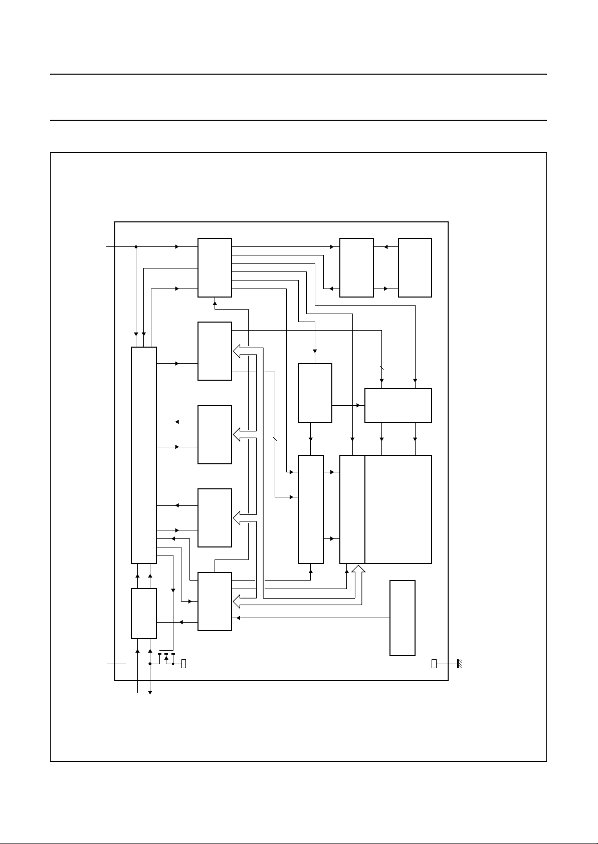
6 BLOCK DIAGRAM
7
WP
SEQUENCER
POINTER
ADDRESS
PCF851 16-3
MBH922
DIVIDER
OSCILLATOR
6
HV
DEC
GENERATOR
SHIFT
REGISTER
C-BUS CONTROL LOGIC
2
I
ADDRESS
COMPARATOR
REGISTER
INPUT
FILTER
n
8
DD
V
6
5
TEST MODE
5
COLUMN DECODER
PAGE REGISTER
PCF85116-3
ROW
(8 × 256 × 8)
EEPROM ARRAY
POWER-ON-RESET
4
Fig.1 Block diagram.
SS
V
SCL
SDA
1997 Apr 02 5
Philips Semiconductors Product specification
2048 × 8-bit CMOS EEPROM with I2C-bus
interface
7 PINNING
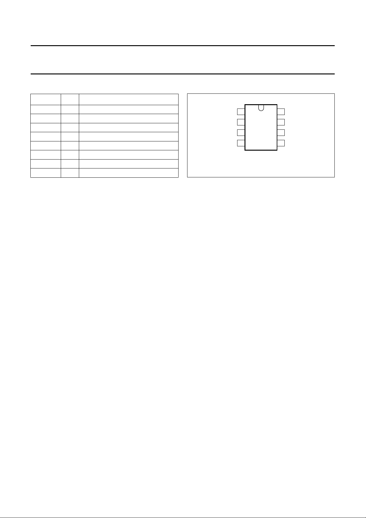
SYMBOL PIN DESCRIPTION
n.c. 1 not connected
n.c. 2 not connected
n.c. 3 not connected
V
SS
SDA 5 serial data input/output (I
SCL 6 serial clock input (I
WP 7 write-protection input
V
DD
8I2C-BUS PROTOCOL
The I2C-bus is for 2-way, 2-line communication between
different ICs or modules. The serial bus consists of two
bidirectional lines: one for data signals (SDA), and one for
clock signals (SCL).
Both the SDA and SCL lines must be connected to a
positive supply voltage via a pull-up resistor.
The following protocol has been defined:
• Data transfer may be initiated only when the bus is not
busy
• During data transfer, the data line must remain stable
whenever the clock line is HIGH. Changes in the data
line while the clock line is HIGH will be interpreted as
control signals.
8.1 Bus conditions
The following bus conditions have been defined:
• Bus not busy: both data and clock lines remain HIGH.
• Start data transfer: a change in the state of the data line,
from HIGH-to-LOW, while the clock is HIGH, defines the
START condition
• Stop data transfer: a change in the state of the data line,
from LOW-to-HIGH, while the clock is HIGH, defines the
STOP condition
• Data valid: the state of the data line represents valid
data when, after a START condition, the data line is
stable for the duration of the HIGH period of the clock
signal. There is one clock pulse per bit of data.
8.2 Data transfer
4 negative supply voltage
2
C-bus)
8 positive supply voltage
2
C-bus)
PCF851 16-3
handbook, halfpage
V
n.c.
n.c.
n.c.
SS
1
2
PCF85116-3
3
4
MBH923
Fig.2 Pin configuration.
Data transfer is unlimited in the read mode.
The information is transmitted in bytes and each receiver
acknowledges with a ninth bit.
Within the I
2
C-bus specifications a low-speed mode (2 kHz
clock rate), a high speed mode (100 kHz clock rate) and a
fast speed mode (400 kHz clock rate) are defined.
The PCF85116-3 operates in all three modes.
By definition a device that sends a signal is called a
‘transmitter’, and the device which receives the signal is
called a ‘receiver’. The device which controls the signal is
called the ‘master’. The devices that are controlled by the
master are called ‘slaves’.
Each byte is followed by one acknowledge bit.
This acknowledge bit is a HIGH level, put on the bus by the
transmitter. The master generates an extra acknowledge
related clock pulse. The slave receiver which is addressed
is obliged to generate an acknowledge after the reception
of each byte.
The master receiver must generate an acknowledge after
the reception of each byte that has been clocked out of the
slave transmitter.
The device that acknowledges has to pull down the SDA
line during the acknowledge clock pulse in such a way that
the SDA line is stable LOW during the HIGH period of the
acknowledge related clock pulse.
Set-up and hold times must be taken into account.
A master receiver must signal an end of data to the slave
transmitter by not generating an acknowledge on the last
byte that has been clocked out of the slave. In this event
the transmitter must leave the data line HIGH to enable the
master generation of the STOP condition.
V
8
DD
WP
7
6
SCL
5
SDA
Each data transfer is initiated with a START condition and
terminated with a STOP condition; the number of the data
bytes, transferred between the START and STOP
conditions is limited to 32 bytes in the E/W mode.
1997 Apr 02 6
 Loading...