


INTEGRATED CIRCUITS
DATA SH EET
PCF84CxxxA family
8-bit microcontrollers
Product specification
Supersedes data of May 1994
File under Integrated Circuits, IC14
1996 Nov 22

Philips Semiconductors Product specification
8-bit microcontrollers PCF84CxxxA family
CONTENTS
1 INTRODUCTION
2 FEATURES
3 GENERAL DESCRIPTION
4 BLOCK DIAGRAM
5 PINNING INFORMATION
5.1 Pinning
5.2 Pin description
6 FUNCTIONAL DESCRIPTION
6.1 Central processing unit
6.2 Program memory
6.3 Data memory
6.3.1 Working registers
6.3.2 Program Counter stack
6.4 Program Counter
6.5 Program Status Word
6.6 Interrupts
6.6.1 External interrupt
6.6.2 I2C-bus/Derivative interrupt
6.6.3 Timer/event counter interrupt
6.7 Timer/event counter 1
6.7.1 Test 1/count input (T1)
6.8 Parallel ports
6.9 I2C-bus interface
6.9.1 Data shift register (S0)
6.9.2 Address register (S0’)
6.9.3 Clock control register (S2)
6.9.4 Status Register (S1)
6.10 Timing
6.11 Oscillator
6.12 Reset
6.12.1 Passive external reset
6.12.2 Active external reset
6.12.3 Internal reset
6.12.4 Reset state
6.13 Reduced power modes
6.13.2 Stop mode
6.14 Derivative logic
7 INSTRUCTION SET
7.1 Instruction map
8 DEFINITIONS
9 LIFE SUPPORT APPLICATIONS
10 PURCHASE OF PHILIPS I2C COMPONENTS
1996 Nov 22 2

Philips Semiconductors Product specification
8-bit microcontrollers PCF84CxxxA family
1 INTRODUCTION
This data sheet describes the shared properties of the
PCF84CxxxA family of microcontrollers. The family
currently consists of:
• PCF84C00
• PCF84C12A; 22A; 42A
• PCF84C21A; 41A; 81A
• PCF84C85A
• PCF84C122; 222; 422; 622; 822
• PCF84C44x; 64x; 84x
• PCF84C846.
For a particular microcontroller, this data sheet should be
read in conjunction with the individual data sheet of the
specific device. Data sheets can be found in
Handbook IC14, “8048-based 8-bit microcontrollers”
The PCD33xxA family of microcontrollers has similar
characteristics to the PCF84CxxxA family, but with lower
minimum operating voltage, DTMF/modem/musical tone
generation and (for most devices) on-chip EEPROM. This
family should be considered for telecom-specific
applications. Please refer to the
sheet.
“PCD33xxA family”
“Data
.
data
3 GENERAL DESCRIPTION
The PCF84CxxxA family of microcontrollers provide up to
8 kbytes of program memory and up to 256 bytes of RAM.
All devices include flexible I/O ports, an 8-bit
programmable timer/event counter and a choice of
single-level vectored interrupts. Most devices feature
2
C-bus compatibility. The instruction set is based on that
I
of the well-known MAB8048. Some of the devices have
functional equivalents in the MAB84xx family of NMOS
controllers. Where the lower power consumption and
higher speed of CMOS provide advantages, the
PCF84CxxxA devices can be used as direct replacements
for their MAB84xx equivalents.
A range of prototyping devices with external program
memory and ‘Piggy-backs’, as well as emulation probes
and prototyping systems are available.
2 FEATURES
• 8-bit CPU, ROM, RAM, I/O all in one package
• Up to 8 kbytes ROM
• Up to 256 bytes RAM
• Over 100 instructions (based on MAB8048) all of
1 or 2 cycles
• 8 or more quasi-bidirectional I/O port lines
• 8-bit programmable timer/event counter 1
• 2 or 3 single-level vectored interrupts: external,
timer/event counter, (I
• Two test inputs, one of which also serves as the external
interrupt input
• I2C-bus serial data interface (most devices)
• Derivative logic (most devices)
• Power-on-reset, Stop and Idle modes
• Supply voltage range: 2.5 to 6 V
• Clock frequency: 1 to 16 MHz
• Operating temperature: −40 to +85 °C
• Manufactured in silicon gate CMOS process.
2
C-bus/derivative)
1996 Nov 22 3

Philips Semiconductors Product specification
8-bit microcontrollers PCF84CxxxA family
4 BLOCK DIAGRAM
MBA283 - 2
P0.7 to P0.0
P1.7 to P1.0
P2.2 to P2.0
3
SDA/P2.3
SCLK
PORT 0
BUFFER
PORT 0
PORT 1
BUFFER
PORT 1
UP TO
8 kbytes
DECODE
RESIDENT ROM
PORT 2
BUFFER
PORT 2
DATACLOCK
FLIP-FLOPS
FLIP-FLOPS
FLIP-FLOPS
13
BANK
MEMORY
FLIP-FLOPS
WORD
STATUS
PROGRAM
LOWER
COUNTER
PROGRAM
HIGHER
COUNTER
PROGRAM
EVENT
TIMER/
COUNTER
32
C-BUS
2
I
INTERFACE
(8)
(5)
Timer
interrupt
(8)
T1
FREQ.
CLOCK
INTERNAL
8
30
848 858878 8
REGISTER 0
REGISTER 1
REGISTER 2
MULTIPLEXER
RAM
ADDRESS
RUPT
LOGIC
INTER -
(8)
REGISTER 2
TEMPORARY
(8)
REGISTER 1
TEMPORARY
(8)
ACCUMULATOR
REGISTER 3
REGISTER 4
REGISTER 5
REGISTER 6
DECOD
REGISTER
&
REGISTER
INSTRUCTION
LOGIC UNIT
ARITHMETIC
POR
V
ON
RESET
POWER
REGISTER 7
8-LEVEL STACK
OPTIONAL SECOND
(VARIABLE LENGTH)
E
INT / T0
DECODER
RESET
DATA STORE
REGISTER BANK
FLAG
CARRY
T1
TIMER
LOGIC
BRANCH
CONDITIONAL
(8)
ADJUST
DECIMAL
external
interrupt
GND
SS
VDDV
POWER
SUPPLY
UP TO 256 bytes
RESIDENT RAM ARRAY
TEST
ACC
ACC BIT
XTAL 2XTAL 1RESETINT / T0
XTAL
OSCILLATOR
CONTROL & TIMING
STOP
INITIALIZE
INTERRUPT
IDLE
handbook, full pagewidth
Fig.1 Block diagram.
1996 Nov 22 4
LOGIC
DERIVATIVE
= type dependent
interrupt
SIO / derivative
Philips Semiconductors Product specification
8-bit microcontrollers PCF84CxxxA family
5 PINNING INFORMATION
5.1 Pinning
For individual pinning configurations consult the data
5.2 Pin description
Table 1 describes the common functions of the devices.
For full details of pin descriptions consult the data sheet of
the specific device.
sheet of the specific device.
Table 1 Common functions
SYMBOL TYPE DESCRIPTION
V
SS
V
DD
P ground
P positive supply voltage
XTAL1 I crystal oscillator/external clock input
XTAL2 O crystal oscillator output
RESET I Reset input
INT/T0 I Interrupt/Test 0 input
T1 I Test 1/count input of 8-bit timer/event counter 1
P0.0 to P0.7 I/O Port 0: quasi-bidirectional I/O lines
P1.0 to P1.7 I/O Port 1: quasi-bidirectional I/O lines
P2.0 to P2.2 I/O Port 2: quasi-bidirectional I/O lines
2
SDA/P2.3 I/O bidirectional data line of the I
SCLK I/O bidirectional clock line of the I
C-bus interface/Port 2: quasi-bidirectional I/O line
2
C-bus interface
1996 Nov 22 5

Philips Semiconductors Product specification
8-bit microcontrollers PCF84CxxxA family
6 FUNCTIONAL DESCRIPTION
6.1 Central processing unit
The PCF84CxxxA family provides an instruction set with
arithmetic, logic, branching, input/output and control
facilities. Special highlights are the instructions for BCD
arithmetic, nibble handling, conditional branches, loop
control (DJNZ) and table look-up (MOVP).
Code and execution efficiency is achieved by using a
maximum of two bytes and two execution cycles per
instruction (see Chapter 7).
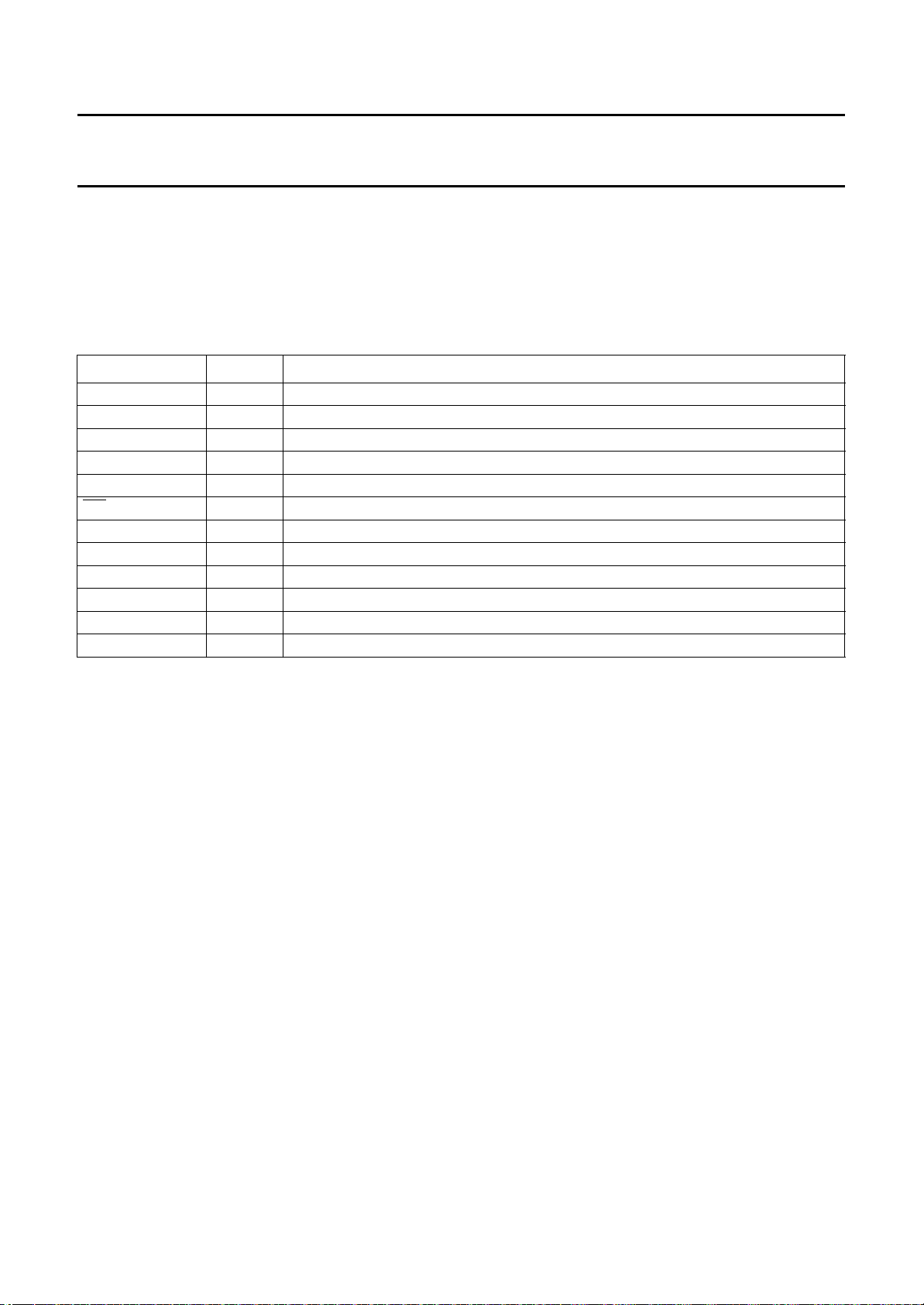
6.2 Program memory
The program memory consists of up to 8 kbytes of
read-only memory (ROM). Each location is directly
addressable by the Program Counter. The program
memory is mask-programmed at the factory. Figure 2
illustrates the program memory map.
Four program memory locations are of special importance:
• Location 0: first instruction to be executed after the
processor is reset
• Location 3: first instruction of an external interrupt
INT/T0) routine
(
• Location 5: first instruction of a I2C-bus/derivative
interrupt routine
• Location 7: first instruction of a timer/event counter
interrupt routine.
Only 11 bits of the 13-bit Program Counter function as a
counter. The two most significant bits can only be preset.
The program memory is therefore, structured into banks of
2 kbytes. Transfer of control to other memory banks is
performed by unconditional branches (JMP) or subroutine
calls (CALL) when another memory bank has been
pre-selected (by SEL MB instruction).
Each program memory bank is further divided into 8 pages
of 256 bytes. Indirect (JMPP) and conditional branches
cannot cross page boundaries.
6.3 Data memory
Data memory consists of up to 256 bytes of random
access memory (RAM). All locations are indirectly
addressable using RAM pointer registers. Up to
16 register locations are directly addressable. Data
memory also includes an 8-level Program Counter stack
addressed by a 3-bit Stack Pointer. All RAM locations
make efficient program loop counters if used with the
decrement register and test instruction (DJNZ). Figure 3
illustrates the data memory map.
6.3.1 W
Locations 0 to 7 are working registers. They are
accessible by efficient one byte/one cycle instructions,
thus making these locations suitable for frequently
accessed intermediate results.
As an alternative to locations 0 to 7, locations 24 to 31
may be used as working registers. Register bank selection
is made by SEL RB0/RB1 instructions. Register bank 1
may be used as an extension of register bank 0, as an
alternative register bank for interrupt service or as general
purpose data memory.
The first two locations of each bank (R0, R1, R0’ and R1’)
serve as RAM pointers that indirectly address all RAM
locations.
6.3.2 P
Locations 8 to 23 may be used as an 8-level Program
Counter stack reserving 2 locations per level, or as
general purpose RAM. The stack (see Fig.5) saves return
addresses and status during interrupt or subroutine
servicing. Nesting of subroutines and/or interrupts is
permitted up to 8-levels deep.
The 3-bit Stack Pointer always points to the next free stack
level. Following device reset, the Stack Pointer points to
level 0 (locations 8 and 9). On each subroutine call (CALL)
or interrupt, the contents of the Program Counter and
bits 4, 6 and 7 of the Program Status Word are transferred
to the level indicated by the Stack Pointer. The Stack
Pointer increments and points to the next free level.
Overflow from level 7 to level 0 occurs after nesting eight
levels deep. Further subroutine calls and/or interrupts
must not occur at this stage since this would result in loss
of program content; overriding level 0 content.
Return from interrupt must be performed by the RETR
instruction, which decrements the Stack Pointer and
restores the Program Counter and Program Status Word,
valid before the interrupt occurred. Return from subroutine
should be performed by the RET instruction. In contrast to
RETR, RET does not restore the Program Status Word.
As a general rule, the use of RETR in conjunction with a
subroutine call is not recommended. The use of RETR
must also be avoided with subroutines called from
interrupt routines because it prematurely terminates the
interrupt state (see Section 6.6).
ORKING REGISTERS
ROGRAM COUNTER STACK
1996 Nov 22 6
Philips Semiconductors Product specification
8-bit microcontrollers PCF84CxxxA family
8191
handbook, halfpage
6143
4095
2048
2047
1024
1023
8
7
6
5
4
3
2
1
0
SEL MB3
SEL MB2
SEL MB1
SEL MB0
location 7: timer/event counter interrupt
vector
location 5: SIO/derivative interrupt
vector
location 3: external interrupt vector
location 0: reset vector
MBA284
255
128
127
64
63
32
31
25
24
23
8
7
1
0
USER
RAM
BANK 1
WORKING
REGISTERS
8 x 8
R1'
R0'
8-LEVEL
STACK
or
USER RAM
16 x 8
BANK 0
WORKING
REGISTERS
8 x 8
R1
R0
MLA616
directly
addressable
when Bank 1
is selected
directly
addressable
when Bank 0
is selected
addressed
indirectly
through pointers
R0, R1, R0', R1'
Fig.2 Program memory map. Fig.3 Data memory map.
saved in
handbook, halfpage
the stack
ACCY
76543
MSB LSB
1
saved in
the stack
RBS PS
Fig.4 Program Status Word.
1996 Nov 22 7
stack pointer
SP
SP1SP
2
21
0
0
MLA617

Philips Semiconductors Product specification
8-bit microcontrollers PCF84CxxxA family
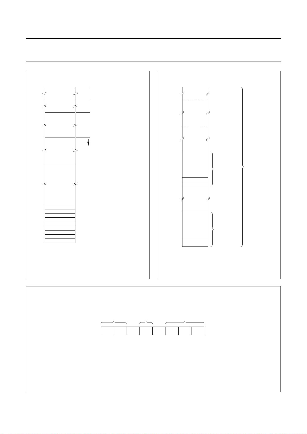
6.4 Program Counter
The 13-bit Program Counter is able to address up to
8 kbytes of ROM (see Fig.6). 11 bits (PC0 to PC10) are
auto-incrementing. The two most significant bits
(PC11 and PC12) must be changed under program
control by SEL MB followed by a JMP or CALL instruction.
6.5 Program Status Word
The Program Status Word (PSW) is an 8-bit register in the
CPU which stores information about the current status of
the microcontroller (see Fig.4).
The PSW bits are:
• Bits 0 to 2: Stack Pointer bits (SP0, SP1, SP2)
• Bit 3: timer Prescaler Select (PS); 0 = modulo-32,
1 = modulo-1 (no prescaling)
• Bit 4: working Register Bank Select (RBS);
0 = register bank 0, 1 = register bank 1
• Bit 5: not used (fixed at 1)
• Bit 6: Auxiliary Carry (AC); half-carry bit generated by an
ADD instruction and used by the decimal adjust
instruction DA A
• Bit 7: Carry (CY); the carry flag indicates that the
previous operation resulted in an overflow of the
Accumulator.
interrupts. Bit 3 can be controlled by MOV PSW, A and
bit 4 by SEL RB instructions. Bit 6 is set and cleared as a
side-effect of ADD and ADDC instructions. Bit 7 is affected
by ADD, ADDC, DA, RLC, RRC, CLR C and CPL C
instructions.
PC
10
DATA MEMORY
LOCATION
PC
PC
PC
8
9
LSB
MEA030
23
22
21
20
19
18
17
16
15
14
13
12
11
10
9
8
STACK
POINTER
handbook, halfpage
111
110
101
100
011
010
001
000
PSW
MSB
7PC6PC5PC4PC3PC2PC1PC0
PCPSW
7
12
6
PSW
PC
11
4
All bits can be read using the MOV A, PSW instruction.
Bits 0, 1 and 2 are affected by CALL, RET, RETR and
handbook, full pagewidth
PC12PC11PC10PC9PC8PC7PC6PC5PC4PC3PC2PC1PC
JMP or CALL instructions transfer the
contents of internal flipflop MBFF0 to PC
and MBBF1 to PC
Fig.6 Program Counter.
Fig.5 Program Counter Stack.
Conventional Program Counter
counts 000H to 7FFH
overflows 7FFH to 000H
(MBFF0) 0 by SELMB0
(MBFF1) 0
(MBFF0) 0 by SELMB1
(MBFF1) 0
(MBFF0) 0 by SELMB2
(MBFF1) 0
(MBFF0) 0 by SELMB3
(MBFF1) 0
0
11
12
MLA694
1996 Nov 22 8

Philips Semiconductors Product specification
8-bit microcontrollers PCF84CxxxA family
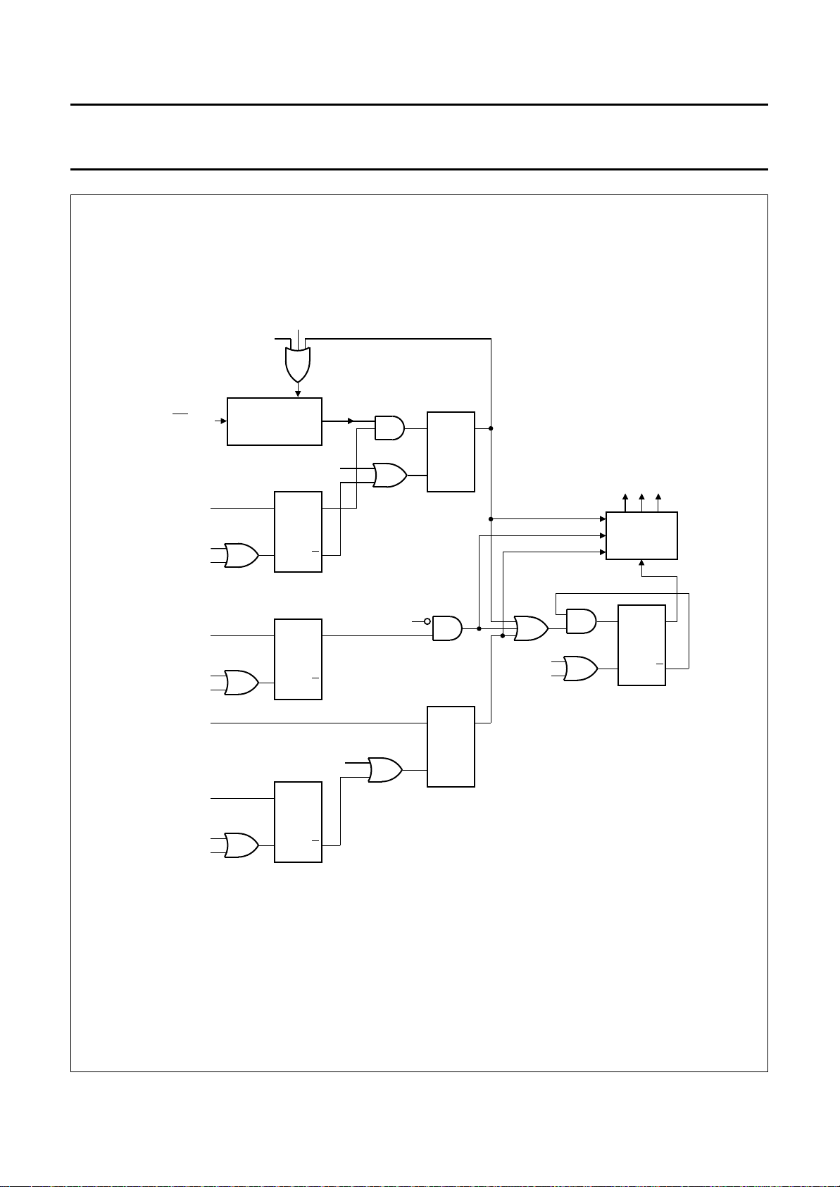
6.6 Interrupts
External, I2C-bus/derivative and timer/event counter
interrupts are handled by the PCF84CxxxA family.
The interrupt mechanism is single level, i.e. an executing
interrupt routine cannot be pre-empted unless by reset.
Further interrupt requests are latched. If several interrupt
requests are detected simultaneously, they are honoured
according to their priority:
• External interrupt (highest priority)
• I2C-bus/derivative interrupt
• Timer/event counter interrupt (lowest priority).
An interrupt request is only sensed if the corresponding
enable flag is set (see Fig.7). When the request is
honoured, the contents of the Program Counter and bits
4, 6 and 7 of the Program Status Word are saved on the
Program Counter stack. The Program Counter is loaded
with the appropriate interrupt vector, thereby indicating the
beginning of the interrupt routine. Since the Accumulator is
not automatically saved, it must be saved and restored by
user software. The interrupt routine must be terminated by
the RETR (return and restore) instruction. At least one
instruction of the main program will then be executed
before another interrupt routine is entered. To avoid
erroneous real-time programs, a few words of caution:
• While the interrupt is in progress, the two most
significant bits of the Program Counter are frozen at
zero. Thus, interrupt routines and subroutines called
from interrupt routines must reside entirely in bank 0.
• The SEL MB instruction must not be used in interrupt
routines and in subroutines called from interrupt
routines. Otherwise, the changed contents of MBFF0
and MBFF1 (see Fig.6) may lead to erroneous JMP and
CALL destinations after return from interrupt.
• Subroutines and nested subroutines called from the
interrupt routine must all end with RET since RETR
clears the Interrupt In Progress flag (IIP), as a side-effect
(see Figs 7 and 8). Further pending interrupts would
then interfere with the interrupt routine in progress.
6.6.1 E
A HIGH-to-LOW transition on the INT/T0 pin is latched in
the digital filter/latch if the LOW state exceeds 7 clock
periods after a HIGH state of more than 4 clock periods.
If the external interrupt is enabled the External Interrupt
Flag (EIF) is also asserted, thus constituting a valid
external interrupt request. As soon as the IIP is clear,
indicating that no interrupt routine is in progress, the
external interrupt is invoked by a forced CALL to
location 3. The EIF is simultaneously cleared (see
Figs 7 and 8). The interrupt routine may acknowledge the
XTERNAL INTERRUPT
interrupt via port lines. Execution of a DIS I (disable
external interrupt) instruction cancels a stored interrupt
request by clearing both the digital filter/latch and the EIF.
6.6.1.1 Interrupt/Test 0 (INT/T0)
The INT/T0 input has two purposes:
• External interrupt input
• Test 0 input.
When used as a Test 0 input (external interrupt disabled)
the conditional branch instruction JT0 will cause a jump if
INT/T0 = 1. The conditional branch instruction JNT0 will
also cause a jump if
must be tied to VDD or VSS.
6.6.2 I
The I2C-bus/derivative interrupt is shared between the
I2C-bus interface (if available) and the derivative logic (if
available). Software polling may be necessary to
determine the origin of a request.
An interrupt condition in the I2C-bus interface and/or the
derivative logic will pull the PIN line LOW. If the
I2C-bus/derivative interrupt is enabled and no interrupt
routine is in progress, the I2C-bus/derivative interrupt
routine will be invoked by a forced CALL to program
memory location 5. The I2C-bus/derivative interrupt
routine must include instructions that will remove the
cause of the I2C-bus/derivative interrupt and thus reset
PIN to its inactive HIGH state (for further details see
Section 6.9). For derivative interrupts, consult the data
sheet of the specific device.
6.6.3 T
If the timer/event counter interrupt is enabled, a
timer/event counter 1 overflow sets the Timer Interrupt
Flag (TIF). As soon as IIP is clear, meaning that no
interrupt routine is in progress, the timer/event counter
interrupt routine is invoked by a forced CALL to program
memory location 7. The TIF is simultaneously cleared (see
Figs 7 and 8). Execution of a DIS TCNTI (disable
timer/event counter interrupt) instruction cancels a stored
interrupt request by clearing TIF.
The timer/event counter interrupt may also be used to
simulate a second external interrupt. After an enable
timer/event counter interrupt (EN TCNTI), the counter
mode is enabled by a STRT CNT instruction which loads
FFH (the state preceding overflow) into the counter.
A positive edge on the T1 pin will overflow the counter and
set TIF.
2
C-BUS/DERIVATIVE INTERRUPT
IMER/EVENT COUNTER INTERRUPT
INT/T0 = 0. If INT/T0 is not used, it
1996 Nov 22 9
Philips Semiconductors Product specification
8-bit microcontrollers PCF84CxxxA family
RESET
handbook, full pagewidth
DIS I
CLEAR
INT / T0
EN I
DIS I
RESET
EN SI
DIS SI
RESET
TIMER
OVERFLOW
EN
TCNT I
DIS
TCNT I
RESET
DIGITAL
FILTER / LATCH
CLEAR EIF
SQ
EI
ENABLE
R
SQ
SI
ENABLE
R
CLEAR TIF
SQ
TI
ENABLE
R
Q
Q
Q
PIN
SQ
EIF
R
SQ
TIF
R
MBA285 - 1
RETR
RESET
CALL EI / CLEAR EIF
CALL SI
CALL TI / CLEAR TIF
INTERRUPT
VECTOR
LOGIC
SQ
IIP
R
Q
Fig.7 Simplified interrupt logic schematic (the R input overrules the S input for all flags).
1996 Nov 22 10

Philips Semiconductors Product specification
8-bit microcontrollers PCF84CxxxA family
handbook, full pagewidth
RESET
FETCH
INSTRUCTION
RETR?
Y
CLEAR IIP
AND RETURN
TO MAIN PROGRAM
N
EN I?
OR
EN TCNT I?
OR
EN SI?
Y
ENABLE
RELEVANT
INTERRUPT
TIMER
OVERFLOW?
N
INT / TO
N
EIF
SET?
N
Y
Y
Y
DIS I?
Y
DISABLE EI
CLEAR FILTER
LATCH AND EIF
SET TF
TI
ENABLED?
N
N
DIS SI?
DISABLE
Y
SET FILTER
NN
DIS
TCNT I?
Y
SI
SET TIF
LATCH
Y
DISABLE TI
AND CLEAR
TIF
EXECUTE
INSTRUCTION
N
FILTER
LATCH
SET?
Y
SET?
PIN = 0?
TIF SET?
Y
N
IIP
N
YN
IIP
SET?
Y
N
N
Y
N
SI
ENABLED?
SET IIP
CLEAR TIF
CALL 007 CALL 005
ENABLED
Y
SET IIP
YN
EI
SET EIF
CLEAR FILTER
LATCH
SET IIP
CLEAR EIF
CALL 003
MLA695
Fig.8 Flow chart illustrating CPU control in the presence of interrupts.
1996 Nov 22 11
 Loading...