

Philips PCF84C85AT Datasheet
INTEGRATED CIRCUITS
DATA SH EET
PCF84C85A
Microcontroller with extended I/O
Product specification
Supersedes data of May 1994
File under Integrated Circuits, IC14
1996 Nov 21

Philips Semiconductors Product specification
Microcontroller with extended I/O PCF84C85A
CONTENTS
1 FEATURES
2 GENERAL DESCRIPTION
3 ORDERING INFORMATION
4 BLOCK DIAGRAM
5 PINNING INFORMATION
5.1 Pinning
5.2 Pin description
6 PARALLEL PORTS
7 INSTRUCTION SET
8 SUMMARY OF DERIVATIVE PORTS AND
REGISTERS
9 ROM MASK OPTIONS
10 HANDLING
11 LIMITING VALUES
12 DC CHARACTERISTICS
13 AC CHARACTERISTICS
13.1 I2C-bus interface characteristics
14 PACKAGE OUTLINES
15 SOLDERING
15.1 Introduction
15.2 DIP
15.2.1 Soldering by dipping or by wave
15.2.2 Repairing soldered joints
15.3 SO and VSO
15.3.1 Reflow soldering
15.3.2 Wave soldering
15.3.3 Repairing soldered joints
16 DEFINITIONS
17 LIFE SUPPORT APPLICATIONS
18 PURCHASE OF PHILIPS I2C COMPONENTS
1996 Nov 21 2
Philips Semiconductors Product specification
Microcontroller with extended I/O PCF84C85A
1 FEATURES
• 8-bit CPU, ROM, RAM, I/O in a single 40-lead package
• 8 kbytes ROM
• 256 bytes RAM
• I2C-bus interface with multi-master capability
• Over 100 instructions (based on MAB8048)
all of 1 or 2 cycles
• 32 quasi-bidirectional I/O port lines
• 8-bit programmable timer/event counter 1
• Three single-level vectored interrupts:
– external
– 8-bit programmable timer/event counter 1
2
C-bus
–I
• Two test inputs, one of which also serves as the external
interrupt input
• Stop and Idle modes
• Logic supply voltage: VDD= 2.5 to 5.5 V
• Clock frequency: 1 to 16 MHz
• Operating temperature: −40 to +85 °C
• Manufactured in silicon gate CMOS process.
2 GENERAL DESCRIPTION
This data sheet details the specific properties of the
PCF84C85A. The shared properties of the PCF84CxxxA
family of microcontrollers are described in the
“PCD84xxxA family”
conjunction with this publication.
The PCF84C85A is a general purpose CMOS
microcontroller with emphasis on input/output. It provides
32 I/O port lines, 8 kbytes of program memory and
256 bytes of RAM. In addition to the 32 I/O port lines, the
microcontroller provides an on-chip I
two-line serial bus extends the microcontroller's
capabilities when implemented with the powerful I2C-bus
peripherals.These include LCD drivers, telecom circuits,
AD/DA converters, clock/calendar circuits, EEPROM and
RAM and are listed in
Peripherals”
The instruction set is based on that of the MAB8048 and is
a sub-set of that listed in the
sheet.
.
data sheet which should be read in
2
C-bus interface. This
“Data Handbook IC12, I2C
“PCF84CXXXA family”
data
3 ORDERING INFORMATION (see note 1)
TYPE
NUMBER
PCF84C85AP DIP40 plastic dual in-line package; 40 leads (600 mil) SOT 129-1
PCF84C85AT VSO40 plastic very small outline package; 40 leads SOT 158-1
Note
1. Please refer to the Order Entry Form (OEF) for this device for the full type number to use when ordering. This type
number will also specify the required program and the ROM mask options.
NAME DESCRIPTION VERSION
PACKAGE
1996 Nov 21 3

Philips Semiconductors Product specification
Microcontroller with extended I/O PCF84C85A
4 BLOCK DIAGRAM
8
DERIVATIVE
DP1.0 to DP1.6
8
DERIVATIVE
DP0.0 to DP0.7
PORT 0
P0.0 to P0.7
8 kbytes
DECODE
RESIDENT ROM
8 8
PORT 1
P1.0 to P1.7
PORT 1
BUFFER
DERIVATIVE
PORT 0
BUFFER
DERIVATIVE
BUFFER
PORT 0
BUFFER
PORT 1
PORT 1
FLIP-FLOPS
PORT 0
FLIP-FLOPS
FLIP-FLOPS
INTERNAL
FLIP-FLOPS
BANK
MEMORY
FLIP-FLOPS
FREQ.
CLOCK
30
WORD
STATUS
PROGRAM
LOWER
COUNTER
PROGRAM
HIGHER
COUNTER
PROGRAM
EVENT
TIMER/
COUNTER
32
T1
8
8
8
5 888 8
88 8
8
8
8
8
REGISTER 0
REGISTER 1
REGISTER 2
MULTIPLEXER
RAM
ADDRESS
REGISTER 1
TEMPORARY
REGISTER 2
TEMPORARY
REGISTER 3
REGISTER 4
REGISTER 5
REGISTER 6
DECOD
REGISTER
&
REGISTER
INSTRUCTION
LOGIC UNIT
ARITHMETIC
REGISTER 7
8-LEVEL STACK
(VARIABLE LENGTH)
DECODER
DATA STORE
REGISTER BANK
OPTIONAL SECOND
E
FLAG
T1
INT / T0
TIMER
BRANCH
CONDITIONAL
ADJUST
DECIMAL
MLA596
256 bytes
RESIDENT RAM ARRAY
TEST
CARRY
ACC
ACC BIT
LOGIC
XTAL 2XTAL 1RESETINT / T0
XTAL
OSCILLATOR
CONTROL & TIMING
INTERRUPT INITIALIZE
handbook, full pagewidth
Fig.1 Block diagram.
C-BUS
2
I
INTERFACE
1
8
8
SDA/P2.3
SCLK
PORT 2
BUFFER
CLOCK DATA
PORT 2
FLIP-FLOPS
1996 Nov 21 4
ACCUMULATOR
timer interrupt
LOGIC
INTERRUPT
SIO/
derivative
interrupt
STOP
external interrupt
IDLE
Philips Semiconductors Product specification
Microcontroller with extended I/O PCF84C85A
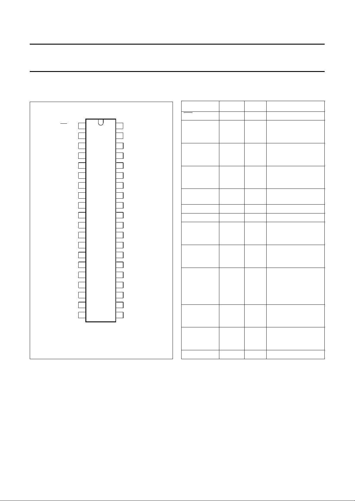
5 PINNING INFORMATION
5.1 Pinning
handbook, halfpage
INT / T0
XTAL1
XTAL2
P0.0
P0.1
P0.2
P0.3
P0.4
P0.5
P0.6
P0.7
P1.0
P1.1
P1.2
P1.3
P1.4
P1.5
P1.6
P1.7
V
SS
1
2
3
4
5
6
7
8
9
10
PCF84C85A
11
12
13
15
16
17
18
19
20
Fig.2 Pin configuration.
MLA597
40
39
38
37
36
35
34
33
32
31
30
29
28
2714
26
25
24
23
22
21
V
DD
T1
SCLK
SDA / P2.3
DP1.6
DP1.5
DP1.4
DP1.3
DP1.2
DP1.1
DP1.0
DP0.7
DP0.6
DP0.5
DP0.4
DP0.3
DP0.2
DP0.1
DP0.0
RESET
5.2 Pin description Table 1 DIP40 and VSO40 packages.
SYMBOL PIN TYPE DESCRIPTION
INT/T0 1 I Interrupt/Test 0
P0.0 to P0.7 2 to 9 I/O 8 bits of Port 0: 8-bit
quasi-bidirectional
I/O port
P1.0 to P1.7 10 to 17 I/O 8 bits of Port 1: 8-bit
quasi-bidirectional
I/O port
XTAL1 18 I XTAL input: crystal
oscillator/external
clock input
XTAL2 19 O XTAL output: crystal
oscillator output
V
SS
20 P ground
RESET 21 I Reset input
DP0.0 to
DP0.7
22 to 29 I/O Derivative Port 0:
quasi-bidirectional
I/O port (8-bit)
DP1.0 to
DP1.6
30 to 36 I/O Derivative Port 1:
quasi-bidirectional
I/O lines (7-bit)
SDA/P2.3 37 I/O bidirectional data line
2
of the I
C-bus
interface; or Port 2
quasi-bidirectional
I/O port (1 bit only)
SCLK 38 I/O bidirectional clock
2
line of the I
C-bus
interface
T1 39 I Test 1: count input of
8-bit timer/event
counter 1
V
DD
40 P positive supply
6 PARALLEL PORTS
Of the standard quasi-bidirectional I/O ports, Port 2 is
incomplete, providing only line SDA/P2.3 that is shared
with the I2C-bus interface. In addition to the standard ports,
two derivative I/O ports are available:
• Derivative Port of 8 lines (DP0.0 to DP0.7)
• Derivative Port of 7 lines (DP1.0 to DP1.6).
Missing bits of incomplete ports, i.e. P2.0 to P2.2 and
DP1.7, are fixed at zero in the corresponding registers.
1996 Nov 21 5
7 INSTRUCTION SET
See
“PCF84CXXXA family”
data sheet for a complete
description of the instruction set.
Philips Semiconductors Product specification
Microcontroller with extended I/O PCF84C85A
8 SUMMARY OF DERIVATIVE PORTS AND REGISTERS Table 2 Derivative Ports.
DERIVATIVE
ADDRESS
00H R DP0L Derivative Port 0 lines
01H R DP1L Derivative Port 1 lines
02H R/W DP0FF Derivative Port 0 flip-flops
03H R/W DP1FF Derivative Port 1 flip-flops
04H −−
Table 3 Derivative Registers.
REGISTER
MNEMONIC
DP0L D0.7 D0.6 D0.5 D0.4 D0.3 D0.2 D0.1 D0.0
DP1L 0 D1.6 D1.5 D1.4 D1.3 D1.2 D1.1 D1.0
DP0FF F0.7 F0.6 F0.5 F0.4 F0.3 F0.2 F0.1 F0.0
DP1FF 0 F1.6 F1.5 F1.4 F1.3 F1.2 F1.1 F1.0
9 ROM MASK OPTIONS
Program/data Any mix of instructions and data up to ROM size of
TYPE
76543210
ROM CODE OPTION
REGISTER
MNEMONIC
DESCRIPTION
8 kbytes.
Port Output
P0.0 to P0.7 standard open-drain push-pull
P1.0 to P1.7 standard open-drain push-pull
SDA/P2.3 − open-drain −
DP0.0 to DP0.7 standard open-drain push-pull
DP1.0 to DP1.7 standard open-drain push-pull
Port State after reset
P0.0 to P0.7 set reset −
P1.0 to P1.7 set reset −
SDA/P2.3 set −−
DP1.0 to DP1.7 set reset −
DP2.0 to DP2.2 set reset −
Oscillator
Transconductance LOW (g
) MEDIUM (gmM) HIGH (gmH)
mL
1996 Nov 21 6
 Loading...