

INTEGRATED CIRCUITS
DATA SH EET
PCF84C21A; PCF84C41A;
PCF84C81A
Telecom microcontrollers
Product specification
Supersedes data of 1995 Jul 14
File under Integrated Circuits, IC14
1996 Nov 20

Philips Semiconductors Product specification
Telecom microcontrollers
CONTENTS
1 FEATURES
2 GENERAL DESCRIPTION
3 ORDERING INFORMATION
4 BLOCK DIAGRAM
5 PINNING INFORMATION
5.1 Pinning
5.2 Pin description
6 INSTRUCTION SET
7 HIGH SINK OUTPUT CURRENTS
8 ROM MASK OPTIONS
9 HANDLING
10 LIMITING VALUES
11 DC CHARACTERISTICS
12 AC CHARACTERISTICS
13 PACKAGE OUTLINES
14 SOLDERING
14.1 Introduction
14.2 DIP
14.2.1 Soldering by dipping or by wave
14.2.2 Repairing soldered joints
14.3 SO
14.3.1 Reflow soldering
14.3.2 Wave soldering
14.3.3 Repairing soldered joints
15 DEFINITIONS
16 LIFE SUPPORT APPLICATIONS
17 PURCHASE OF PHILIPS I2C COMPONENTS
PCF84C21A; PCF84C41A;
PCF84C81A
1996 Nov 20 2
Philips Semiconductors Product specification
Telecom microcontrollers
1 FEATURES
• Manufactured in silicon gate CMOS process
• 8-bit CPU, ROM, RAM, I/O in a 28-lead package
• 2 kbyte ROM, 64 byte RAM (PCF84C21A)
• 4 kbyte ROM, 128 byte RAM (PCF84C41A)
• 8 kbyte ROM, 256 byte RAM (PCF84C81A)
• I2C-bus interface with multi-master capability
• Over 100 instructions (based on MAB8048) all of
1 or 2 cycles
• 20 quasi-bidirectional I/O Port lines
• High sink current capability on the 8 lines of Port 1
• 8-bit programmable timer/event counter 1
• 3 single-level vectored interrupts:
– external
– 8-bit programmable timer/event counter 1
2
C-bus
–I
• Two test inputs, one of which also serves as the external
interrupt input
• Stop and Idle modes
• Supply voltage: 2.5 to 5.5 V
• Clock frequency: 1 to 16 MHz
• Operating temperature: −40 to +85 °C.
PCF84C21A; PCF84C41A;
PCF84C81A
2 GENERAL DESCRIPTION
This data sheet details the specific properties of the
PCF84C21A, PCF84C41A and PCF84C81A. The shared
properties of the PCF84CxxxA family of microcontrollers
are described in the
which should be read in conjunction with this publication.
The PCF84C21A, PCF84C41A and PCF84C81A are
general purpose CMOS microcontrollers with 2 kbytes,
4 kbytes and 8 kbytes of program memory and 64,128 and
256 bytes of RAM, respectively. In addition to 20 I/O port
lines, the microcontrollers provide an on-chip I
interface. This two-line serial bus extends the
microcontroller capabilities when implemented with the
powerful I2C-bus peripherals. These include LCD drivers,
I/O expanders, telecom circuits, ADC and DAC converters,
clock/calendar circuits, EEPROM and RAM and are listed
in
“Data Handbook IC12, I2C Peripherals”.
The instruction set is based on that of the MAB8048 and
is a sub-set of that listed in the
sheet.
“PCF84CxxxA family”
“PCF84CxxxA family”
data sheet
2
C-bus
data
3 ORDERING INFORMATION (see note 1)
TYPE NUMBER
NAME DESCRIPTION VERSION
PCF84C21AP DIP28 plastic dual in-line package; 28 leads (600 mil) SOT117-1
PCF84C41AP
PCF84C81AP
PCF84C21AT SO28 plastic small outline package; 28 leads; body width 7.5 mm SOT136-1
PCF84C41AT
PCF84C81AT
Note
1. Please refer to the Order Entry Form (OEF) for these devices for the full type number to use when ordering. This type
number will also specify the required program and the ROM mask options.
1996 Nov 20 3
PACKAGE
Philips Semiconductors Product specification
Telecom microcontrollers
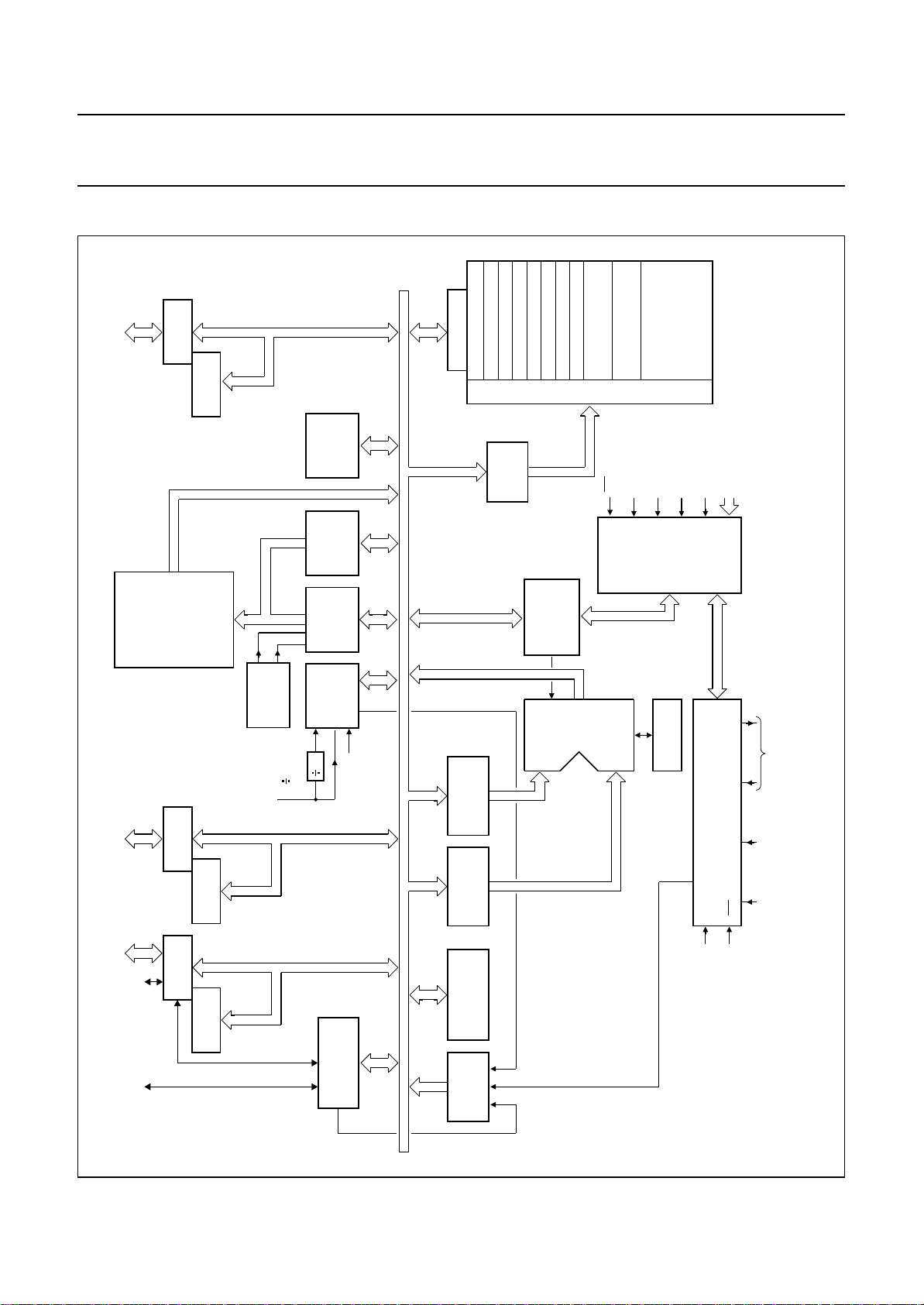
4 BLOCK DIAGRAM
8
PORT 0
P0.0 to P0.7
BUFFER
PORT 0
FLIP-FLOPS
WORD
STATUS
PROGRAM
LOWER
COUNTER
PROGRAM
8
MULTIPLEXER
REGISTER 0
REGISTER 1
REGISTER 2
REGISTER 3
RAM
ADDRESS
REGISTER
PCF84C21A; PCF84C41A;
PCF84C81A
REGISTER 4
REGISTER 5
REGISTER 6
REGISTER 7
DECOD
8 LEVEL STACK
REGISTER BANK
OPTIONAL SECOND
(VARIABLE LENGTH)
E
FLAG
T 1
INT / T0
TIMER
BRANCH
CONDITIONAL
DATA STORE
CARRY
LOGIC
64 bytes
128 bytes
(PCF84C21A)
RESIDENT RAM ARRAY
TEST
ACC
ACC BIT
256 bytes
(PCF84C41A)
(PCF84C81A)
MBB561 - 1
2 kbytes
4 kbytes
(PCF84C21A)
RESIDENT ROM
8
P1.0 to P1.7P2.0 to P2.2
3
SDA/P2.3
SCLK
8 kbytes
DECODE
(PCF84C41A)
(PCF84C81A)
PORT 1
BUFFER
PORT 1
FLIP-FLOPS
PORT 2
BUFFER
PORT 2
DATA
FLIP-FLOPS
CLOCK
BANK
MEMORY
FLIP-FLOPS
30
FREQ.
CLOCK
INTERNAL
HIGHER
PROGRAM
EVENT
TIMER/
32
C-BUS
2
I
5888 8
COUNTER
8
COUNTER
T1
8
4
8
INTERFACE
88 8
8
8
REGISTER 1
TEMPORARY
REGISTER 2
TEMPORARY
ACCUMULATOR
timer interrupt
LOGIC
INTERRUPT
&
DECODER
REGISTER
INSTRUCTION
LOGIC UNIT
ARITHMETIC
SIO/
interrupt
derivative
ADJUST
DECIMAL
CONTROL &
STOP
external interrupt
XTAL 2XTAL 1RESETINT / T0
TIMING
IDLE
OSCILLATOR
INTERRUPT INITIALIZE
handbook, full pagewidth
Fig.1 Block diagram of PCF84C21A; PCF84C41A and PCF84C81A.
Fig.0 Block diagram of PCF84C21A, PCF84C41A and PCF84C81A.
1996 Nov 20 4
Philips Semiconductors Product specification
Telecom microcontrollers
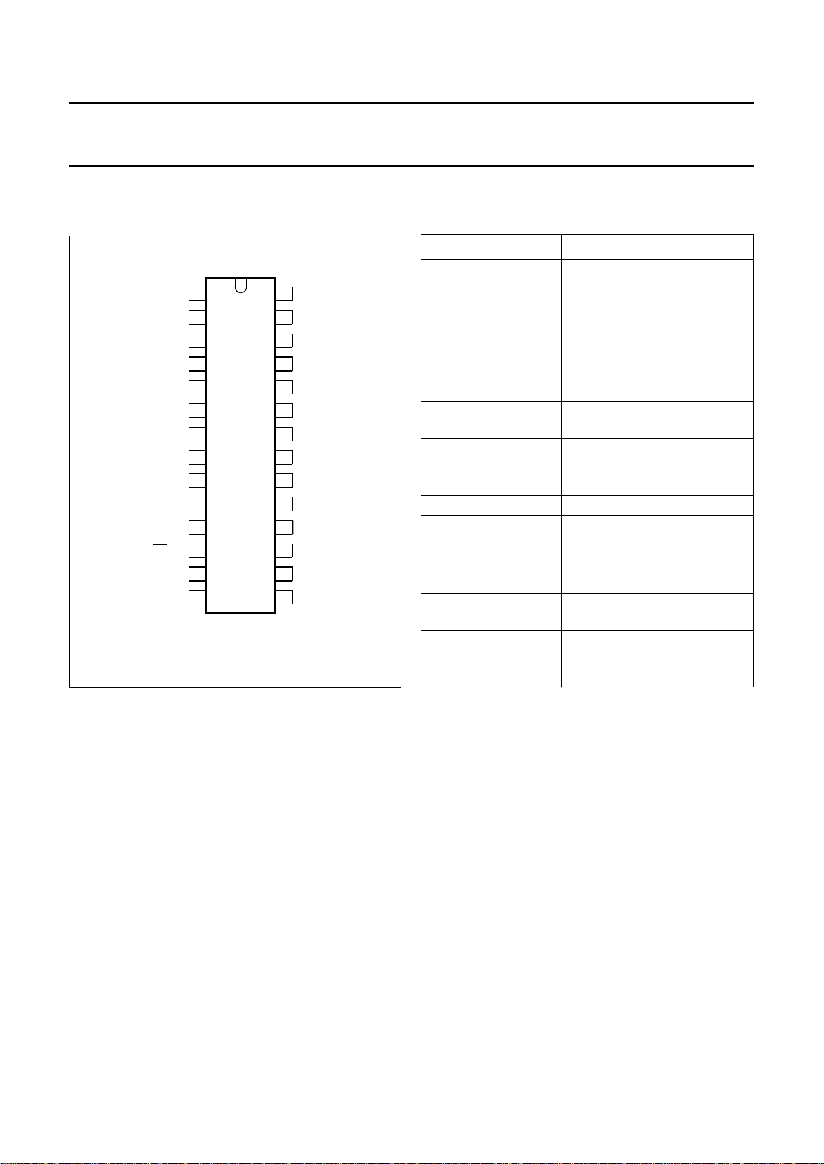
5 PINNING INFORMATION
5.1 Pinning
1
P2.2
SDA/P2.3
INT/T0
2
3
SCLK
4
P0.0
5
P0.1
6
P0.2
PCF84C21A
7
P0.3
P0.4
P0.5
P0.6
P0.7
T1
V
SS
PCF84C41A
PCF84C81A
8
9
10
11
12
13
MBB562
Fig.2 Pin configuration.
28
27
26
25
24
23
22
21
20
19
18
17
16
1514
V
DD
P2.1
P2.0
P1.7
P1.6
P1.5
P1.4
P1.3
P1.2
P1.1
P1.0
RESET
XTAL2
XTAL1
PCF84C21A; PCF84C41A;
PCF84C81A
5.2 Pin description
Table 1 DIP28 and SO28 packages
SYMBOL PIN FUNCTION
P2.2 1 1 bit of Port 2: 4-bit
quasi-bidirectional I/O port
SDA/P2.3 2 bidirectional data line of the
SCLK 3 bidirectional clock line of the
P0.0 to P0.7 4 to 11 8 bits of Port 0: 8-bit
INT/T0 12 Interrupt/Test 0
T1 13 Test 1/count input of 8-bit
V
SS
14 ground
XTAL1 15 crystal oscillator input or
XTAL2 16 crystal oscillator output
RESET 17 Reset input
P1.0 to P1.7 18 to 25 8 bits of Port 1: 8-bit
P2.0 to P2.1 26 to 27 2 bits of Port 2: 4-bit
V
DD
28 positive supply
2
I
C-bus interface, or 1 bit of
Port 2: 4-bit quasi-bidirectional
I/O port
2
C-bus interface
I
quasi-bidirectional I/O port
timer/event counter 1
external clock input
quasi-bidirectional I/O port
quasi-bidirectional I/O port
6 INSTRUCTION SET
ROM is restricted to 2 kbytes for the PCF84C21A and
4 kbytes for the PCF84C41A. Therefore, the instructions
SEL MB1/2/3 for the PCF84C21A, and the instructions
SEL MB2/3 for the PCF84C41A should be avoided, as
they would define non-existing program memory banks.
As RAM is limited to 64 bytes for the PCF84C21A and to
128 bytes for the PCF84C41A, care should be taken to
avoid accesses to non-existing RAM locations.
See the “
PCF84CxxxA family
” data sheet for a complete
description of the instruction set.
1996 Nov 20 5
7 HIGH SINK OUTPUT CURRENTS
The Port 1 outputs of these devices are designed for high
current drive in the logic 0 state. They are capable of
driving 10 mA loads and higher. Applications include drive
for small relays and light-emitting diodes (LEDs).
To avoid overload, care should be taken that the total
Port 1 current averages less than 80 mA, i.e. an average
of 10 mA per Port 1 line. Refer to Chapter “Limiting values”
which specifies an upper limit of 100 mA for ISS.
 Loading...