

Philips PCF84C12AP, PCF84C12AT Datasheet

INTEGRATED CIRCUITS
DATA SH EET
PCF84C12A
8-bit microcontroller
Product specification
Supersedes data of 1996 Nov 20
File under Integrated Circuits, IC14
1998 May 11

Philips Semiconductors Product specification
8-bit microcontroller PCF84C12A
CONTENTS
1 FEATURES
2 GENERAL DESCRIPTION
3 ORDERING INFORMATION (see note 1)
4 BLOCK DIAGRAM
5 PINNING INFORMATION
5.1 Pinning
5.2 Pin description
6 INSTRUCTION SET
7 ROM MASK OPTIONS
8 HANDLING
9 LIMITING VALUES
10 DC CHARACTERISTICS
11 AC CHARACTERISTICS
12 PACKAGE OUTLINES
13 SOLDERING
13.1 Introduction
13.2 DIP
13.3 SO
14 DEFINITIONS
15 LIFE SUPPORT APPLICATIONS
1998 May 11 2
Philips Semiconductors Product specification
8-bit microcontroller PCF84C12A
1 FEATURES
• Manufactured in silicon gate CMOS process
• 8-bit CPU, ROM, RAM, I/O in a 20-lead package
• 1 kbyte ROM
• 64 byte RAM
• Over 100 instructions (based on MAB8048) all of
1 or 2 cycles
• 13 quasi-bidirectional I/O port lines
• 8-bit programmable timer/event counter 1
• Two single-level vectored interrupts:
– external
– 8-bit programmable timer/event counter 1
• Two test inputs, one of which also serves as the external
interrupt input
• Stop and Idle modes
• Supply voltage: 2.5 to 5.5 V
• Clock frequency: 1 to 16 MHz
• Operating temperature: −40 to +85 °C.
3 ORDERING INFORMATION
2 GENERAL DESCRIPTION
This data sheet details the specific properties of the
PCF84C12A. The shared properties of the PCF84CxxxA
family of microcontrollers are described in the
“PCF84CxxxA family”
conjunction with this publication. Note that the devices
described in this data sheet do not feature I2C-bus
compatibility or derivative logic, so the information given in
the family data sheet about these features can be ignored.
The PCF84C12A is a general purpose CMOS
microcontroller with 1 kbyte of program memory.
It includes 64 bytes of RAM and 13 I/O port lines.
The instruction set is based on the MAB8048 and is a
sub-set of that listed in the
sheet.
data sheet, which should be read in
“PCF84CxxxA family”
data
TYPE NUMBER
PCF84C12AP DIP20 plastic dual in-line package; 20 leads (300 mil) SOT146-1
PCF84C12AT SO20 plastic small outline package; 20 leads; body width 7.5 mm SOT163-1
Note
1. Please refer to the Order Entry Form (OEF) for these devices for the full type number to use when ordering. This type
number will also specify the required program and ROM mask options.
(1)
NAME DESCRIPTION VERSION
PACKAGE
1998 May 11 3
This text is here in white to force landscape pages to be rotated correctly when browsing through the pdf in the Acrobat reader.This text is here in
_white to force landscape pages to be rotated correctly when browsing through the pdf in the Acrobat reader.This text is here inThis text is here in
white to force landscape pages to be rotated correctly when browsing through the pdf in the Acrobat reader. white to force landscape pages to be ...
1998 May 11 4
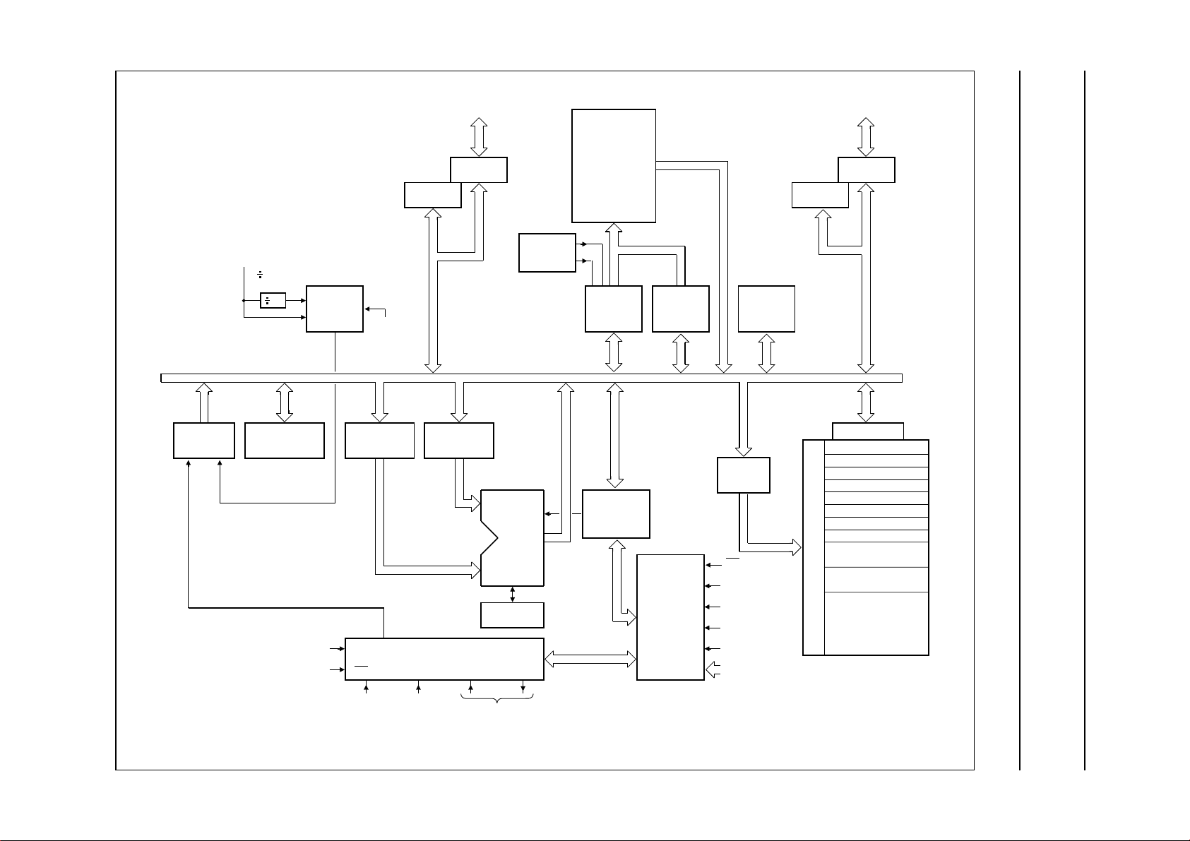
4 BLOCK DIAGRAM
8-bit microcontroller PCF84C12A
Philips Semiconductors Product specification
INTERRUPT
LOGIC
INTERNAL
CLOCK
FREQ.
30
32
8
ACCUMULATOR
timer interrupt
external interrupt
COUNTER
STOP
IDLE
TIMER/
EVENT
INTERRUPT
TEST 1
TEMPORARY
REGISTER 1
P1.0 to P1.4
PORT 1
BUFFER
PORT 1
FLIP-FLOPS
5
888 8 8
TEMPORARY
REGISTER 2
CONTROL & TIMING
INITIALIZE
3
ARITHMETIC
LOGIC UNIT
DECIMAL
ADJUST
XTAL 2XTAL 1RESETINT / T0
OSCILLATOR
MEMORY
BANK
FLIP-FLOPS
(8)
RESIDENT ROM
1 kbyte
(PCF84C12A)
2 kbytes
(PCF84C22A)
4 kbytes
(PCF84C42A)
DECODE
HIGHER
PROGRAM
COUNTER
5 888 8
INSTRUCTION
REGISTER
&
DECODER
LOWER
PROGRAM
COUNTER
CONDITIONAL
BRANCH
LOGIC
PROGRAM
STATUS
WORD
RAM
ADDRESS
REGISTER
INT / T0
TEST 1
TIMER
FLAG
CARRY
ACC
ACC BIT
TEST
PORT 0
FLIP-FLOPS
D
E
C
O
D
E
RESIDENT RAM ARRAY
P0.7 to P0.0
PORT 0
BUFFER
MULTIPLEXER
REGISTER 0
REGISTER 1
REGISTER 2
REGISTER 3
REGISTER 4
REGISTER 5
REGISTER 6
REGISTER 7
8 LEVEL STACK
(VARIABLE LENGTH)
OPTIONAL SECOND
REGISTER BANK
DATA STORE
64 bytes
MBC951
Fig.1 Block diagram of PCF84C12A.
handbook, full pagewidth
Philips Semiconductors Product specification
8-bit microcontroller PCF84C12A
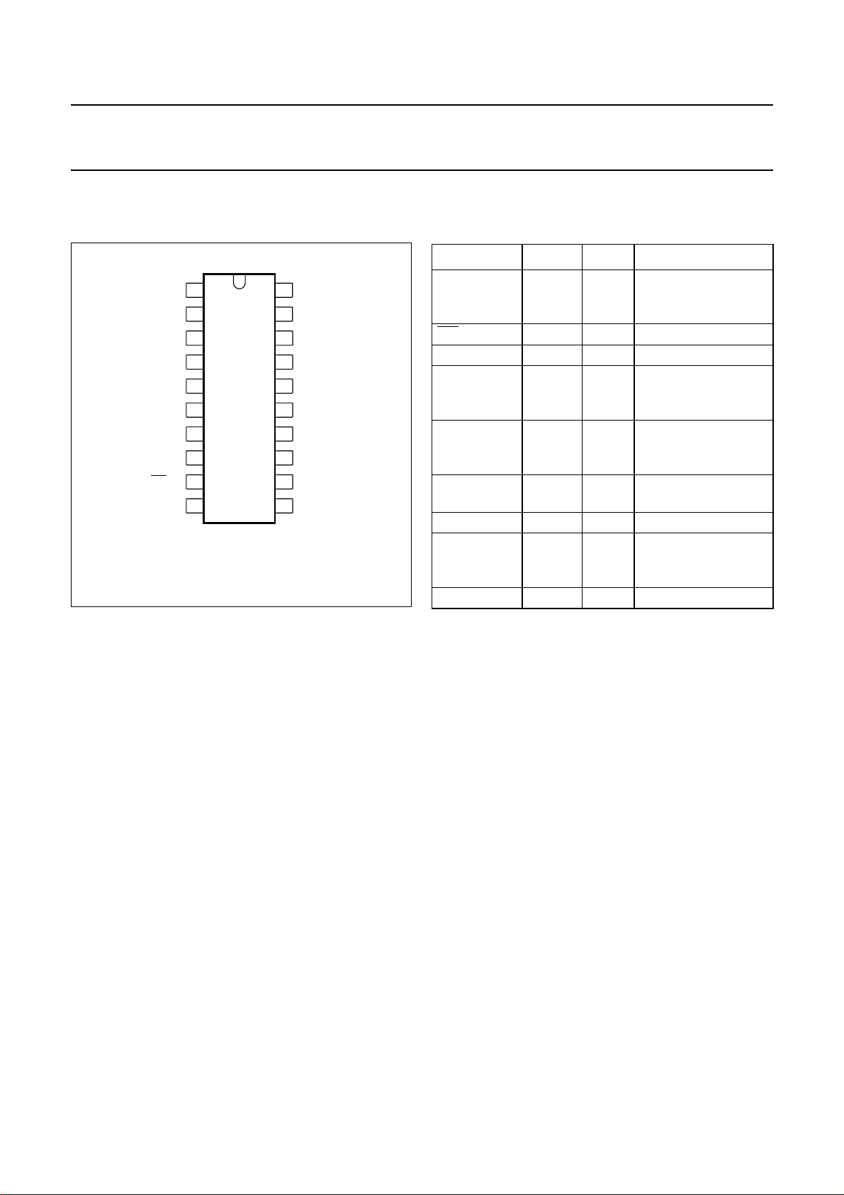
5 PINNING INFORMATION
5.1 Pinning
handbook, halfpage
P0.0
P0.1
P0.2
P0.3
P0.4
P0.5
P0.6
P0.7
INT/T0
V
SS
1
2
3
4
5
PCF84C12A
6
7
8
9
10
Fig.2 Pin configuration.
MBK778
20
19
18
17
16
15
14
13
12
11
V
DD
P1.4
P1.3
P1.2
P1.1
P1.0
RESET
XTAL2
XTAL1
T1
5.2 Pin description
Table 1 DIP20 and SO20 packages
SYMBOL PIN TYPE DESCRIPTION
P0.0 to P0.7 1 to 8 I/O Port 0: 8-bit
quasi-bidirectional
I/O port
INT/T0 9 I Interrupt/Test 0
V
SS
10 P ground
T1 11 I Test 1/count input of
8-bit timer/event
counter 1
XTAL1 12 I crystal oscillator
input or external
clock input
XTAL2 13 O crystal oscillator
output
RESET 14 I reset input
P1.0 to P1.4 15 to 19 I/O Port 1: 4-bit
quasi-bidirectional
I/O port
V
DD
20 P positive supply
6 INSTRUCTION SET
Since the I2C-bus interface, Port 2 and derivative logic are
not provided, instructions associated with these functions
are not available.
ROM space is restricted to 1 kbyte for the PCF84C12A.
Therefore, the instructions SEL MB1/2/3 should be
avoided as they would define non-existing program
memory banks.
As RAM space is limited to 64 bytes, care should be taken
to avoid accesses to non-existing RAM locations.
Refer to the
“PCF84CxxxA family”
data sheet, for a
complete description of the instruction set.
1998 May 11 5
 Loading...