

Philips pcf5083 DATASHEETS

INTEGRATED CIRCUITS
DATA SH EET
PCF5083
GSM signal processing IC
Objective specification
File under Integrated Circuits, IC17
1996 Oct 29

Philips Semiconductors Objective specification
GSM signal processing IC PCF5083
CONTENTS
1 FEATURES
2 GENERAL DESCRIPTION
3 APPLICATIONS
4 ORDERING INFORMATION
5 BLOCK DIAGRAM
6 PINNING INFORMATION
6.1 Pinning
6.2 Pinning description
7 OVERVIEW OF THE GSM CHIP SET
7.1 General
7.2 The role of the PCF5083
8 FUNCTIONAL DESCRIPTION TIMER CORE
8.1 Clock generator
8.2 ON/OFF Logic
8.2.1 Mobile switch-on procedure
8.2.2 Mobile switch-off procedure
8.2.3 OFF/Watchdog Timer
8.3 Timing Generator
8.3.1 The Quarterbit Counter
8.3.2 Normal Mode
8.3.3 Sleep Mode
8.4 RF-IC Interface Bus
8.4.1 Frequency Setting Channel
8.4.2 Gain Control Channel
8.4.3 Immediate Control Channel
8.4.4 Operation Modes and Control Registers
8.5 IOM®-2 Interface
8.5.1 IOM®-2 Clock Generation
8.5.2 IOM®-2 Master Unit
8.5.3 Monitor Channel Transmitter Protocol
8.5.4 Monitor Channel Receiver Protocol
8.5.5 Command/Indication Channel Transmitter
8.5.6 Command/Indication Channel Receiver
8.5.7 Audio Interface
8.5.8 External IOM®-2 Interface
8.6 MMI Interface
8.6.1 RS232 Interface
8.6.2 MMI power-down Interface
8.7 General purpose parallel I/O-port
8.8 Real Time Clock
8.8.1 Setting the real time clock
9 DESCRIPTION OF THE DSP CORE
9.1 Interface description
9.1.1 Baseband Digitizer Interface
9.1.2 GMSK Modulator Interface
9.1.3 Audio and Data Interface
9.1.4 Audio interface
9.1.5 Terminal adaptor interface for data services
9.1.6 System controller interface
9.1.7 Event Counter Clock
9.1.8 Usage of General Purpose I/O Pins
9.1.9 Power saving modes
9.2 Message Interface to the System Controller
9.2.1 Execution of GSM baseband procedures
9.2.2 No Operation (NOP) command
9.2.3 Soft resetting the DSP
9.2.4 Error handling
9.3 GSM baseband procedures
9.3.1 Procedure description
9.3.2 Performance of GSM baseband procedures
9.4 Software applications
9.4.1 Receiving a CCH block
9.4.2 Transmitting a CCH block
9.4.3 FB search for timing synchronization
9.4.4 Processing a TCH/FS multiframe
10 MICROCONTROLLER INTERFACE
10.1 Register Set for the Timer Core
10.2 Interrupt Logic
11 RESET
12 JTAG TEST INTERFACE
13 TEST AND EMULATION MODES
14 LIMITING VALUES
15 DC CHARACTERISTICS
16 AC CHARACTERISTICS
17 APPLICATION INFORMATION
18 PACKAGE OUTLINE
19 SOLDERING
19.1 Introduction
19.2 Reflow soldering
19.3 Wave soldering
19.4 Repairing soldered joints
20 DEFINITIONS
21 LIFE SUPPORT APPLICATIONS
1996 Oct 29 2

Philips Semiconductors Objective specification
GSM signal processing IC PCF5083
1 FEATURES
• Fabricated in a 0.5 µm CMOS process with 3-layer
metal
• LQFP128 package (SOT420AA-2)
• 3.3 V operation
• Low power
• Embedded DSP core for all GSM specific signal
processing tasks:
– 16-bit fixed point DSP
– 19.5 MHz or external clock operation
– Flexible power-down modes
– 5 kbyte on-chip program or data RAM
– 2 kbyte on-chip data ROM
– 16 kbyte on-chip program ROM
– Fully pre-programmed modules for GSM baseband
tasks including all data channels
– Dedicated GSM signal processor with application
specific hardware for: equalisation, channel
encoding/decoding for all traffic and control channels
and encryption/decryption (A5/1 and A5/2
algorithms)
– Tone and side-tone generation
• GSM Hardware Timer and Interface core:
– Power saving Sleep mode for GSM mobiles
– Programmable TDMA timing and power-down
signals with 0.25 bit resolution
– Three wire serial control bus for fast programming of
RF ICs and synthesizers
®
– IOM
-2 interface for external accessories, host
software download and support of the Digital Audio
Interface (DAI)
– RS232 interface for the man machine interface
controller
– Man machine interface power-down control
– Power supply control logic with Watchdog Timer
– Real time clock and calendar running on 32.768 kHz
– 6-bit general purpose I/O port
• Reduced swing 13 MHz main clock input
• On-chip PLL to derive the DSP and microcontroller clock
• 8-bit, 68000 compatible host interface with three
interrupt lines
• Boundary scan interface in accordance with
“IEEE Standard 1149.1-1990”
2 GENERAL DESCRIPTION
The PCF5083 GSM Signal Processing IC is a dedicated
VLSI circuit; fabricated in a 0.5 µm CMOS process. It has
been designed for baseband signal processing tasks for
the Pan European Global System for Mobile
telecommunication (GSM). The PCF5083 is part of the
second generation Philips Semiconductors GSM chip set.
The PCF5083 consists of an embedded 16-bit DSP core
for all GSM specific signal processing tasks and a Timer
and Interface core which contains many peripheral
functions to simplify the system design.
3 APPLICATIONS
The PCF5083 is suitable for use in GSM mobile stations or
hand-helds.
.
4 ORDERING INFORMATION
TYPE NUMBER
NAME DESCRIPTION VERSION
PCF5083H/F2 LQFP128 plastic low profile quad flat package; 128 leads; (PCF5083-2B) SOT420-1
PCF5083H/001/F2 LQFP128 plastic low profile quad flat package; 128 leads; (PCF5083-2C) SOT420-1
PCF5083H/5V2/F3 LQFP128 plastic low profile quad flat package; 128 leads; (PCF5083-3A) SOT420-1
1996 Oct 29 3
PACKAGE
Philips Semiconductors Objective specification
GSM signal processing IC PCF5083
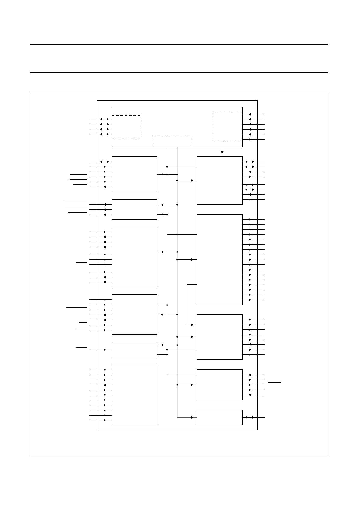
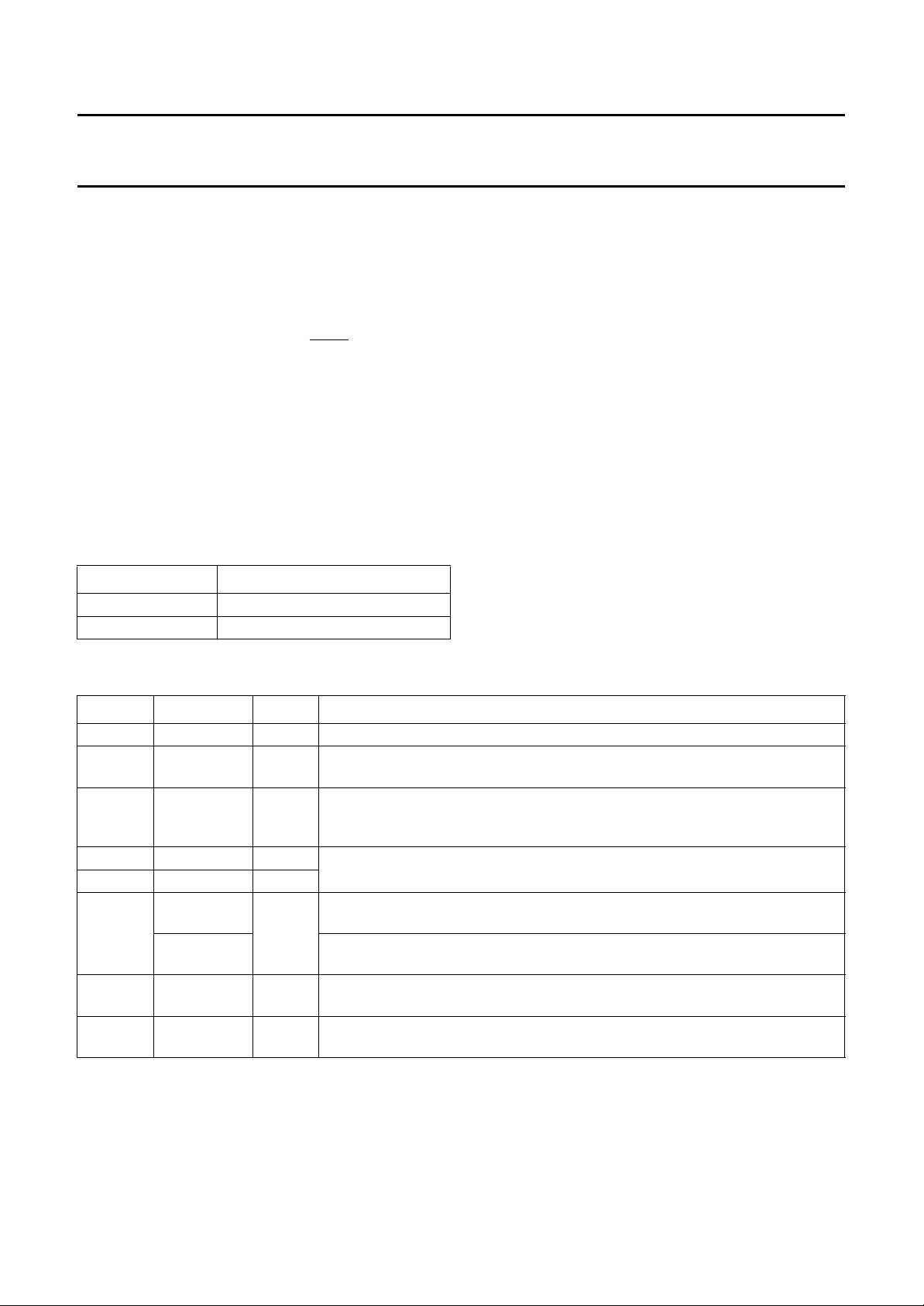
5 BLOCK DIAGRAM
handbook, full pagewidth
IO1/AEN
IO2
IO3/IRQN2
IO4/DTX
HD0 to HD7
HA0 to HA6
HR/W
HCEN_T
HCEN_D
DTACK
FRAME_INT
COMB_INT
HIPR_INT
CKI
CKO
CLK13M
CLK20M
DCLK
CLKSEL
RSTP
CLK32I
CLK32O
CLK32K
ONKEY
AUXON
LOWVOLT
POWON
NPOWON
RST
RSTO
RSTC
EMBEDDED
I/O-PORT
HOST
INTERFACE
INTERRUPT
LOGIC
CLOCK
GENERATOR
AND
PLL
ON / OFF
LOGIC
REAL TIME
CLOCK
DSP-CORE
HOST PORT
AUDIO INTERFACE
SERIAL
X-PORT
AND
Y-PORT
IOM-2
INTERFACE
AND
TIMING
GENERATOR
RF-IC
INTERFACE
SIXCLK
SIXEN
SIXD
SOXCLK
SOXEN
SOXD
FSC
DCL
DU
DD
AFS
ACLK
ADI
ADO
RXON
TXON
BEN
PDRX1
PDRX2
PDTX1
NPDTX1
NPDTX2
PDBIAS
NPDBIAS
PDSYN
TXKEY1
TXKEY2
GPON1
GPON2
REFON
NREFON
RFCLK
RFEN1
RFEN2
RFEN3
RFEN4
RFDI
RFDO
RFE
TCK
TMS
TDI
TDO
TRSTN
TCKIO
TCE
TSCK1
TSCK2
DSPEN
TIMEN
JTAG
AND
TEST
Fig.1 Block diagram.
1996 Oct 29 4
MMI
INTERFACE
PARALLEL
PORT
RXD
TXD
MMIEN
MMICLK
MMIIREQ
PIO1 to PIO5
MGE284
Philips Semiconductors Objective specification
GSM signal processing IC PCF5083
6 PINNING INFORMATION
6.1 Pinning
handbook, full pagewidth
TCE
PIO1
PIO2
PIO3
PIO4
PIO5
BEN
TXON
RXON
V
SS1
V
DD1
PDRX1
PDRX2
PDTX1
NPDTX1
V
DD2
V
SS2
NPDTX2
PDBIAS
NPDBIAS
PDSYN
TXKEY1
TXKEY2
DSPEN
TIMEN
RSTC
RSTO
V
DD1
CLK32O
CLK32I
V
SS1
ONKEY
AFS
ACLK
124
123
DD1VSS1
V
122
121
HIPR_INT
CLK13M
119
120
FRAME_INT
COMB_INT
CLK20M
118
117
116
ADO
TSCK1
ADI
TSCK2
128
127
126
125
1
2
3
4
5
6
7
8
9
10
11
12
13
14
15
16
17
18
19
20
21
22
23
24
25
26
27
28
29
30
31
32
SS2VDD2
V
SOXEN
SOXD
115
114
113
112
PCF5083
SIXEN
SIXD
SOXCLK
111
110
109
SIXCLK
DTACK
108
107
HD7
HR/W
HCEN_D
106
105
104
HD6
103
HD5
102
HD4
101
DD1VSS1
V
999897
100
HD3
HD2
96
95
94
93
92
91
90
89
88
87
86
85
84
83
82
81
80
79
78
77
76
75
74
73
72
71
70
69
68
67
66
65
HD1
HD0
HA6
HA5
HA4
HA3
HA2
HA1
HA0
IO4/DTX
IO3/IRQN2
IO2
IO1/AEN
HCEN_T
TCK
V
SS2
V
DD2
TRSTN
TCKIO
TDO
TDI
TMS
V
DDPLL
CKI
V
DD1
V
SS1
CKO
V
SSPLL
CLKSEL
RSTP
DCLK
REFON
33343536373839404142434445464748495051525354555657585960616263
DU
DD
FSC
DCL
MMICLK
AUXON
LOWVOLT
POWON
NPOWON
RST
TXD
CLK32K
RXD
MMIEN
MMIIREQ
Fig.2 Pin configuration - PCF5083-2B and PCF5083-2C.
1996 Oct 29 5
SS2
V
DD1
V
SS1
V
DD2
V
RFCLK
RFEN1
RFEN2
RFEN3
DD2
V
RFEN4
RFDI
SSPLL
V
RFE
RFDO
64
GPON1
GPON2
NREFON
MGE282
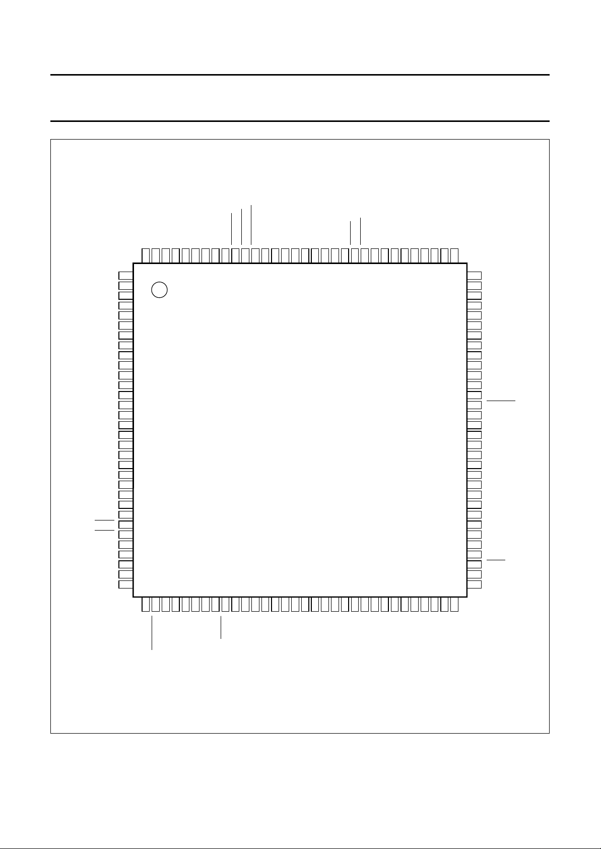
Philips Semiconductors Objective specification
GSM signal processing IC PCF5083
handbook, full pagewidth
TCE
PIO1
PIO2
PIO3
PIO4
PIO5
BEN
TXON
RXON
V
SS1
V
DD1
PDRX1
PDRX2
PDTX1
NPDTX1
V
DD2
V
SS2
NPDTX2
PDBIAS
NPDBIAS
PDSYN
TXKEY1
TXKEY2
DSPEN
TIMEN
RSTC
RSTO
V
DD1
CLK32O
CLK32I
V
SS1
ONKEY
AFS
ACLK
124
123
DD1VSS1
V
122
121
HIPR_INT
CLK13M
119
120
FRAME_INT
COMB_INT
CLK20M
118
117
116
ADO
TSCK1
ADI
TSCK2
128
127
126
125
1
2
3
4
5
6
7
8
9
10
11
12
13
14
15
16
17
18
19
20
21
22
23
24
25
26
27
28
29
30
31
32
SS2VDD2
V
SOXEN
SOXD
115
114
113
112
PCF5083
SIXEN
SIXD
SOXCLK
111
110
109
SIXCLK
DTACK
108
107
HD7
HR/W
HCEN_D
106
105
104
HD6
103
HD5
102
HD4
101
DD1VSS1
V
999897
100
HD3
HD2
96
95
94
93
92
91
90
89
88
87
86
85
84
83
82
81
80
79
78
77
76
75
74
73
72
71
70
69
68
67
66
65
HD1
HD0
HA6
HA5
HA4
HA3
HA2
HA1
HA0
IO4/DTX
IO3/IRQN2
IO2
IO1/AEN
HCEN_T
TCK
V
SS2
V
DD2
TRSTN
TCKIO
TDO
TDI
TMS
V
DDPLL
CKI
V
DD1
V
SS1
CKO
V
SSPLL
CLKSEL
RSTP
DCLK
REFON
33343536373839404142434445464748495051525354555657585960616263
DU
FSC
DCL
DD
AUXON
LOWVOLT
POWON
NPOWON
RST
TXD
CLK26M
RXD
MMIEN
MMIIREQ
MMICLK
Fig.3 Pin configuration - PCF5083-3A.
1996 Oct 29 6
SS2
V
DD1
V
SS1
V
DD2
V
RFCLK
RFEN1
RFEN2
RFEN3
DD2
V
RFEN4
RFDI
SSPLL
V
RFE
RFDO
64
GPON1
GPON2
NREFON
MGD706

Philips Semiconductors Objective specification
GSM signal processing IC PCF5083
6.2 Pinning description SYMBOL PIN I/O DESCRIPTION
TCE 1 I Test Clock Enable (active HIGH); tied to V
PIO1 to PIO5 2 to 6 I/O General purpose parallel port (3-state output).
BEN 7 O Baseband Port Enable (active HIGH, 3-state).
TXON 8 O Modulator window enable (active HIGH, 3-state).
RXON 9 O Receiver window enable (active HIGH, 3-state).
V
V
SS1
DD1
10 Ground I/O pin.
11 Supply I/O pin.
PDRX1 12 O Receiver Power-down 1 (active HIGH, 3-state).
PDRX2 13 O Receiver Power-down 2 (active HIGH, 3-state).
PDTX1 14 O Transmitter Power-down 1 (active HIGH, 3-state).
NPDTX1 15 O Inverted output of PDTX1 (active LOW, 3-state).
V
V
DD2
SS2
16 Supply core.
17 Ground core.
NPDTX2 18 O Transmitter Power-down 2 (active LOW, 3-state).
PDBIAS 19 O Transmitter power supply Power-down (active HIGH, 3-state).
NPDBIAS 20 O Inverted output of PDBIAS (active LOW, 3-state).
PDSYN 21 O Synthesizer Power-down (active HIGH, 3-state).
TXKEY1 22 O Power ramping control (active HIGH, 3-state).
TXKEY2 23 O Power module control (active HIGH, 3-state).
DSPEN 24 I DSP Test Mode Enable (active HIGH). PCF5083-2B includes an internal
pull-down resistor. PCF5083-2C does not include an internal pull-down resistor.
TIMEN 25 I Timer Test Mode Enable (active HIGH). PCF5083-2B includes an internal
pull-down resistor. PCF5083-2C does not include an internal pull-down resistor.
RSTC 26 I Asynchronous Reset - real time clock (active LOW, CMOS level Schmitt trigger
input).
RSTO 27 I Asynchronous Reset - ON/OFF logic (active LOW, CMOS level Schmitt trigger
input).
V
DD1
28 Supply I/O pin.
CLK32O 29 O 32.768 kHz crystal oscillator output.
CLK32I 30 I 32.768 kHz crystal oscillator input.
V
SS1
31 Ground I/O pin.
ONKEY 32 I ON/OFF Key input (active HIGH, CMOS level Schmitt trigger input with internal
pull-down resistor).
during normal operation.
SS
1996 Oct 29 7

Philips Semiconductors Objective specification
GSM signal processing IC PCF5083
SYMBOL PIN I/O DESCRIPTION
AUXON 33 I Auxiliary Switch on input (active HIGH, CMOS level Schmitt trigger input).
LOWVOLT 34 I Low battery indication (active LOW, CMOS level Schmitt trigger input).
POWON 35 O Power Regulator on (active HIGH).
NPOWON 36 O Power Regulator on (active LOW).
RST 37 I Asynchronous Reset for timer section (active LOW, CMOS level Schmitt trigger
input).
CLK32K 38 O The 32.768 kHz CMOS level output for PCF5083-2B and PCF5083-2C.
CLK26M The 26 MHz CMOS level output for PCF5083-3.
TXD 39 O RS232 transmit data output (open-drain output).
RXD 40 I RS232 receive data input.
MMIEN 41 O RS232 input buffer full indication (active LOW, open-drain output).
MMIREQ 42 I MMI clock request (active HIGH, CMOS level Schmitt trigger input).
MMICLK 43 O MMI clock 13 MHz.
FSC 44 I/O IOM
DCL 45 I/O IOM
DU 46 I IOM
DD 47 O IOM
V
V
V
V
SS2
DD1
SS1
DD2
48 Ground core.
49 Supply I/O pin.
50 Ground I/O pin.
51 Supply core.
RFCLK 52 O RF−IC interface shift clock (3-state).
RFEN1 53 O RF−IC Interface Enable 1(active LOW, 3-state).
RFEN2 54 O RF−IC Interface Enable 2 (active LOW, 3-state).
RFEN3 55 O RF−IC Interface Enable 3 (active LOW, 3-state).
RFEN4 56 O RF−IC Interface Enable 4 (active LOW, 3-state).
V
DD2
V
SSPLL
57 Supply core.
58 Ground for PLL.
RFDI 59 I RF−IC Interface data in.
RFDO 60 O RF−IC Interface data out (3-state).
RFE 61 O RF−IC Interface Enable (active HIGH, 3-state).
NREFON 62 O Reference oscillator power-down (active LOW, 3-state).
®
-2 frame pulse (3-state).
®
-2 clock (3-state).
®
-2 data input (CMOS level Schmitt trigger input).
®
-2 data output (open drain output).
1996 Oct 29 8

Philips Semiconductors Objective specification
GSM signal processing IC PCF5083
SYMBOL PIN I/O DESCRIPTION
GPON1 63 O Sleep mode power-down 1 (active HIGH, 3-state).
GPON2 64 O Sleep mode power-down 2 (active HIGH, open-drain output).
REFON 65 O Sleep mode power-down 3 (active HIGH, 3-state).
DCLK 66 I External DSP clock input.
RSTP 67 I PLL reset (active LOW with internal pull-down resistor).
CLKSEL 68 I Timer clock source select.
V
SSPLL
CKO 70 O Low swing input buffer output.
V
SS1
V
DD1
CKI 73 I Reference clock input, low swing input 13 kHz.
V
DDPLL
TMS 75 I JTAG port mode select (with internal pull-down resistor).
TDI 76 I JTAG port data input (with internal pull-down resistor).
TDO 77 O JTAG port data output.
TCKIO 78 I Auxiliary test signal - tied to V
TRSTN 79 I JTAG port reset (with internal pull-down resistor).
V
DD2
V
SS2
TCK 82 I JTAG port clock input (with internal pull-down resistor).
HCEN_T 83 I Host Interface Enable - Timer core (active LOW).
IO1/AEN 84 I/O DSP general purpose I/O used for voice port control (CMOS level I/O). The
IO2 85 I/O DSP general purpose I/O used for voice port control (CMOS level I/O). The
IO3/IRQN2 86 I/O DSP general purpose I/O or Interrupt Request Input 2 (CMOS level I/O). The
IO4/DTX 87 I/O DSP general purpose I/O (CMOS level I/O, external pull-up resistor required).
HA0 to HA6 88 to 94 I Host Interface Address.
HD0 to HD3 95 to 98 I/O Host Interface Data (3-state).
69 Ground for PLL.
71 Ground I/O pin.
72 Supply I/O pin.
74 Supply for PLL.
80 Supply core.
81 Ground core.
PCF5083-3 has its own internal pull-up resistor however, both the PCF5083-2B
and PCF5083-2C require a pull-up resistor.
PCF5083-3 has its own internal pull-up resistor however, both the PCF5083-2B
and PCF5083-2C require a pull-up resistor.
PCF5083-3 has its own internal pull-up resistor however, both the PCF5083-2B
and PCF5083-2C require a pull-up resistor.
during operation.
SS
1996 Oct 29 9

Philips Semiconductors Objective specification
GSM signal processing IC PCF5083
SYMBOL PIN I/O DESCRIPTION
V
SS1
V
DD1
HD4 to HD7 101 to 104 I/O Host Interface data (3-state).
HR/W 105 I Host Interface Write Enable.
HCEN_D 106 I Host Interface Enable - DSP core (active LOW).
DTACK 107 O Host port acknowledge - used as DTACK from DSP core (active LOW , open-drain
SIXCLK 108 I DSP serial input port X clock (CMOS level Schmitt trigger input).
SIXEN 109 I DSP serial input port X enable.
SIXD 110 I DSP serial input port X data.
SOXCLK 111 I DSP serial output port X clock (CMOS level Schmitt trigger input).
V
DD2
V
SS2
SOXEN 114 I DSP serial output port X enable.
SOXD 115 O DSP serial output port X data (3-state).
CLK20M 116 O 19.5 MHz CMOS level output.
FRAME_INT 117 O TDMA frame interrupt (active LOW, open drain output).
COMB_INT 118 O Combined interrupt (active LOW, open drain output).
HIPR_INT 119 O High Priority Interrupt (active LOW, open drain output).
CLK13M 120 O 13 MHz CMOS level output.
V
SS1
V
DD1
AFS 123 I/O Audio Interface frame sync signal (3-state).
ACLK 124 I/O Audio Interface Clock (3-state).
ADI 125 I Audio Interface Data In, RS232 clock if enabled.
ADO 126 O Audio Interface Data Out (3-state).
TSCK1 127 I Test Clock 1 - tied to V
TSCK2 128 I Test Clock 2 - tied to V
99 Ground I/O pin.
100 Supply I/O pin.
output).
112 Supply core.
113 Ground core.
121 Ground I/O pin.
122 Supply I/O pin.
during normal operation.
SS
during normal operation.
DD2
1996 Oct 29 10

Philips Semiconductors Objective specification
GSM signal processing IC PCF5083
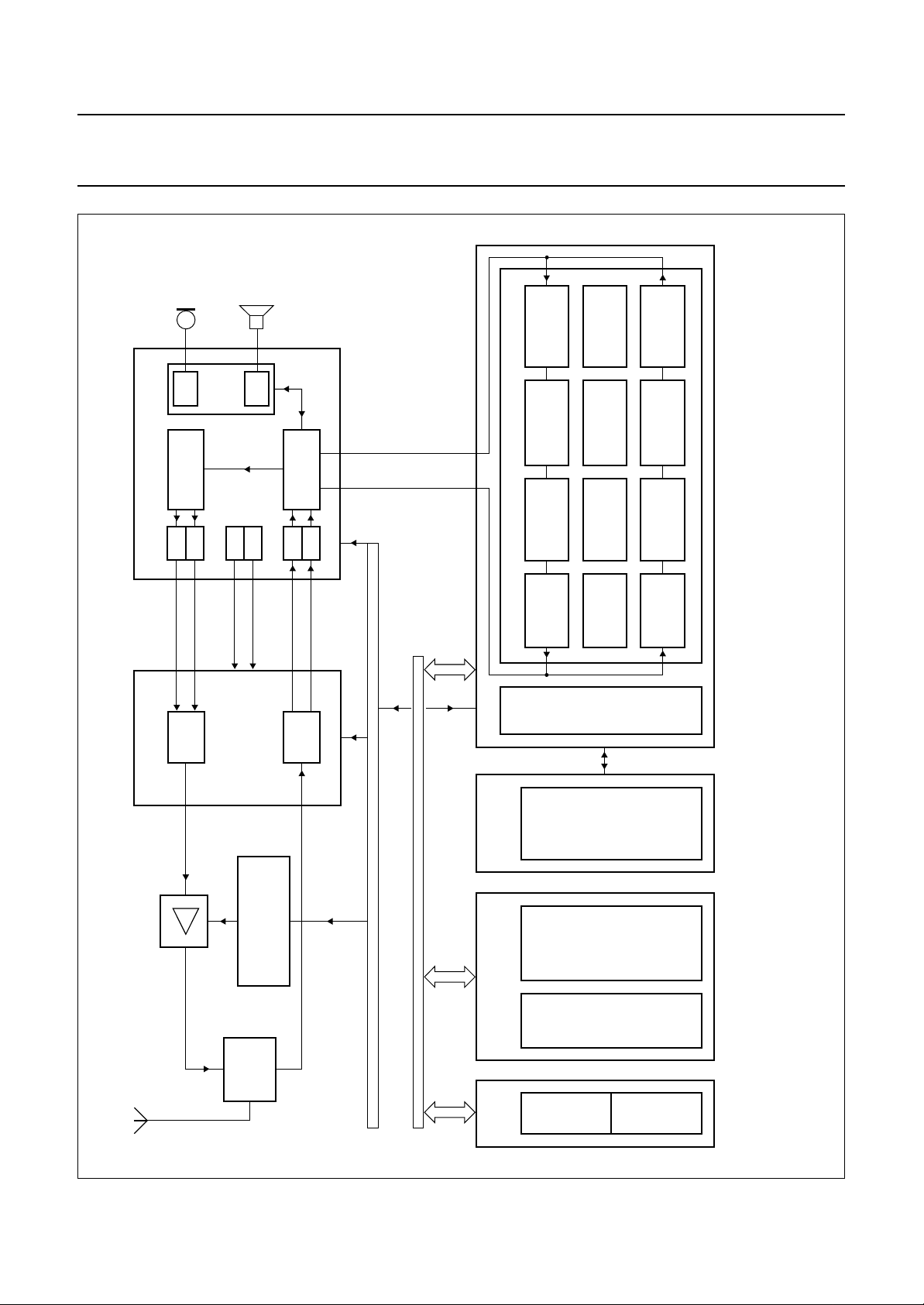
7 OVERVIEW OF THE GSM CHIP SET
7.1 General
The chip set’s high-level architectural modularity ensures
that it can be easily adapted to meet various market
requirements in terms of hardware and software. Figure 4
is a simplified block diagram of a GSM terminal using the
Philips Semiconductors chip set.
The receiver converts the antenna input signal from
890 to 915 MHz down into a complex baseband signal
consisting of an in-phase (I) and a quadrature
component (Q). In order to deal with the high dynamic
range from −104 to −10 dBm, the receiver provides an
AGC input controlled by the layer 1 software in the System
Controller. The complex baseband signal is connected to
the input of the PCF5072 baseband interface IC. This IC
samples the I and Q components at the GSM bit clock
(270 kHz) with an accuracy of approximately 2 × 13 bits.
The equalizer is responsible for the following tasks:
• Channel impulse response estimation and bit
synchronization by means of the training sequence
• Adaptive channel equalization with a modified Maximum
Likelihood Sequence Estimation (MLSE) approach that
produces a bit-by-bit soft decision information (Channel
Measurement Information (CMI)
• Channel impulse response adaption and frequency
offset estimation.
After decryption the channel decoder performs
convolutional and block decoding. Depending on the
logical channel in use, there are decoding schemes for
TCH/F (FACCH/F), SACCH and SDCCH.
The speech decoder synthesises the audio signal from the
received bit stream. Updating of comfort noise parameters
occurs each time a valid Silence Descriptor (SID) is
received. Comfort noise is inserted during periods of
speech pauses. Substitution and muting of lost or bad
frames is implemented.
The full rate speech encoder collects speech samples of
13-bit uniform PCM format (104 kbits/s) and compresses
them to 13 kbits/s according to the linear predictive coding,
long term prediction, Regular Pulse Excitation (RPE-LTP).
Discontinuous Transmission (DTX) is available (voice
activity detection, background acoustic noise).
To protect the data from transmission errors, block and
convolutional coders form the channel encoder. The
encoding modules relates to the logical channels (e.g.
RACH, TCH/F (FACCH/F), SDCCH/SACCH).
After encryption the burst builder generates either Normal
Bursts (NB) or Access Bursts (AB). The bit-stream is then
modulated with a GMSK modulator (Gaussian Minimum
Shift Keying) and upconverted in a quadrature mixer to
890 to 915 MHz.
The on-chip GSM timer generates all power-down and
control signals for the receiver, the transmitter, the
P90CL301 System Controller and the PCF5072 baseband
interface IC.
The System Controller (P90CL301) services all HW
interfaces and performs the signalling software contained
in the GSM layer stack (with L1, L2, L3, O&M, UAP,
SIMAP etc).
The voiceband ADCs and DACs of the PCF5072 perform
the conversion between the analog audio signals and the
digital domain.
7.2 The role of the PCF5083
The PCF5083 is a dedicated VLSI circuit offering
baseband signal processing tasks for the Pan European
Global System for Mobile telecommunication (GSM). The
PCF5083 can be applied in GSM mobile stations or
hand-helds. The embedded DSP core is optimized for
GSM baseband functions and contains an on-chip
program ROM featuring the following tasks:
• Full rate speech coding/decoding including VAD/DTX
(
“GSM 06 series”
• Encryption/decryption according to both A5/1 and A5/2
algorithms (
• Burst building supporting access burst and normal burst
(
“GSM Rec. 5.02”
• Frequency Correction Burst (FCB) detection and
evaluation
• Synchronization burst (SCH) detection
• BCCH monitoring of neighbouring cells
• Channel coding/decoding and
interleaving/de-interleaving (
– Broadcast Channels (BCH): SCH, BCCH
– Common Control Channels (CCCH): PCH, RACH,
AGCH
– Dedicated Control Channels (DCH): SDCCH,
SACCH
– Traffic Channels (TCH): TCH/FS, TCH/F2.4,
TCH/F4.8, TCH/F9.6, TCH/H4.8 and TCH/H2.4
– Associated Control Channels (ACCH): FACCH and
SACCH
)
“GSM Rec. 3.20, 3.21”
)
“GSM Rec. 5.03”
)
) for:
1996 Oct 29 11

Philips Semiconductors Objective specification
GSM signal processing IC PCF5083
• Equalization for normal and synchronization bursts
• Power measurement of serving and neighbouring cells
• Tone and side-tone generation.
2.5 kbytes of RAM are free for downloading of additional
software modules e.g. rate adaptation, handsfree, voice
recognition.
The DSP communicates via two serial ports to the
baseband interface IC and to the IOM®-2 Interface and
Voice Port for speech and data transmission. For
command and data transfer it is connected to a
microcontroller via its 8-bit Host Port and the
68000 compatible Host Interface. The I/O port of the DSP
core provides four general purpose I/O lines. Some of the
port lines are used as dedicated control signals.
The Timer and Interface functions include a GSM specific
hardware timer and a couple of interface functions which
simplify system design and keep the chip count to a
minimum.
The Timing Generator provides the TDMA burst timing and
power on/off signals for the RF transmitter, RF receiver,
synthesizer, DSP and baseband interface IC. The timing
signals can be programmed with an accuracy of a
quarterbit (1⁄
programmable.
The RF-IC Interface is used to program the RF ICs and the
synthesizer. It is compatible with the Philips ‘Three Wire
Bus’ and other standards. The bus consists of clock, data
and several enable lines to transfer data between the
PCF5083 and the connected devices. ICs of one family
share the same enable line. Their unique address is a part
of the data stream. ICs of different families use separate
enable lines.
The PCF5083 includes an IOM®-2 Interface to connect
external accessories e.g. a handsfree set. It may be used
as a software download interface and provides access for
the Digital Audio Interface during Type Approval.
The Audio Interface provides the connection between a
local codec, the IOM®-2 Bus and the DSP.
The ON/OFF Logic performs the basic power-up and
power-down switching function for the whole mobile. It
controls the supply voltage switches for the terminal. The
on/off conditions are controlled via the operators
keyboard, a low voltage battery indication circuit, the
Watchdog Timer or an auxiliary switch on input for general
purpose use.
TDMA frame). Their output polarity is
500
The man-machine interface section includes a dedicated
RS232 interface and generates a 13 MHz clock for the
keyboard and card reader controller. If this controller is
inactive, the clock is stopped to save power. If the
controller requests service, the clock is switched on again.
The PCF5083 includes a 6-bit general purpose parallel
port to control system functions. One bit of the port is used
on-chip to provide a reset signal for the DSP core.
The PCF5083 is accessed via its 8-bit, 68000 compatible
Host Interface. Separate chip enable lines for the DSP and
the Timer core are available. The DSP core provides a
signal to be used as DTACK for maximum speed
operation. Three interrupt lines are provided for the
microcontroller.
The PCF5083 requires two clock signals. The 13 MHz
main clock is used internally to generate the TDMA timing
and as a reference clock for the on-chip PLL. A second
clock of 32.768 kHz is used for a real time clock/calendar,
a Watchdog Timer and to provide timing in a power
reducing Sleep mode. During this mode TDMA timing is
maintained with slow running, high accuracy counters,
while all timing signals are kept inactive to save power.
The on-chip PLL generates three clocks (13, 39 and
52 MHz) which are manipulated to generate the internal
DSP clock (19.5 MHz), a 19.5 MHz output (CLK20M) and
a 26 MHz output (CLK26M, only version 3) used by the
microcontroller and other system components. The
13 MHz PLL output is used by the Timing Generator in
addition to being fed back to the PLL. The nominal duty
cycle of the PLL outputs is 50%, independent of the
reference clock characteristics. The PLL clock outputs
may be used for all system components requiring a
symmetric input clock therefore leading to reduced
tolerance requirements for the duty cycle of the reference
clock.
Other ICs of the Philips second generation GSM chipset
are:
• P90CL301: 16-bit 68000 compatible microcontroller
• TDA8005: SIM/MMI-Controller
• PCF5072: Baseband Interface and Audio Codec
• SA1638: IF processing IC
• SA1620: RF processing IC (900 MHz)
• UMA1019: Synthesizer
• PCF5075: Power amplifier controller
• BGY20x: UHF Power Amplifier Module family.
1996 Oct 29 12
Philips Semiconductors Objective specification
GSM signal processing IC PCF5083
MGE283
PCF5083
ook, full pagewidth
ADC
GMSK
PCF5072SA1620 and SA1638
MODULATOR
DAC
DAC
I
Q
TX
DAC
PCM
codec
DAC
DAC
AFC
AGC
TRANSCEIVER
DSP
ADC
I
RX
INTERFACE
ADC
Q
audio
interface
BBI
(IOM-2)
8-bit parallel port
SPEECH
ENCODER
CHANNEL
ENCODER
DSP CORE
A5/1 + A5/2
ENCRYPTION
BURST
BUILDING
CORE
TIMER
TONE AND
SIDE TONE
GENERATION
SYSTEM
INTERFACE
CONTROLLER
MONITORING
NISATION
SYNCHRO-
SPEECH
DECODER
CHANNEL
DECODER
A5/1 + A5/2
DECRYPTION
EQUALISER
BGY20x
PCF5075
CONTROLLER
POWER AMPLIFIER
FILTER
DUPLEX
transceiver control bus
system control bus
1996 Oct 29 13
TDA8005P90CL301MEMORY
RAM
SIM,
DISPLAY,
KEYBOARD
PERIPHERY
CPU
SYSTEM
Fig.4 Simplified block diagram of a GSM terminal with the PCF5083.
ROM
Philips Semiconductors Objective specification
GSM signal processing IC PCF5083
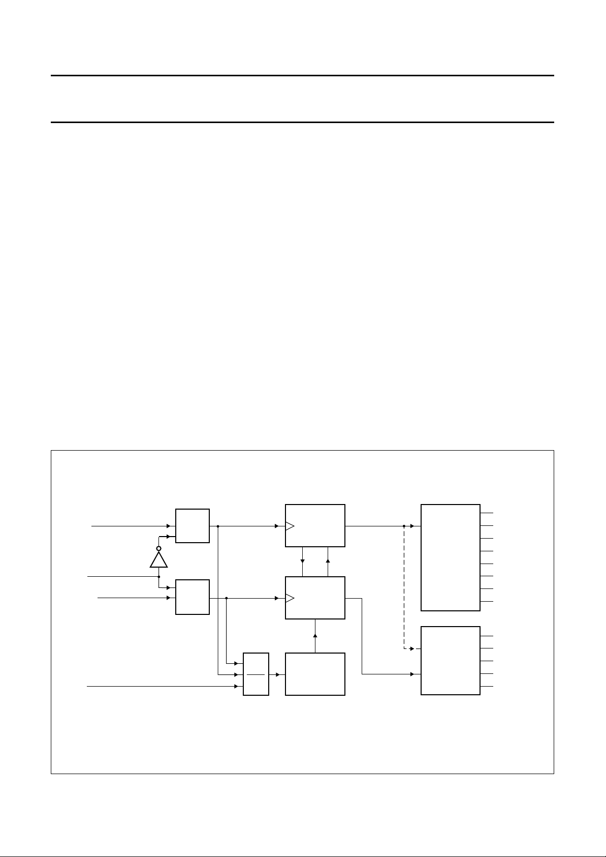
8 FUNCTIONAL DESCRIPTION TIMER CORE
8.1 Clock generator
The Clock Generator consists of a low swing input buffer
for the 13 MHz reference clock, a PLL as frequency
multiplier and a 32.768 kHz crystal oscillator. The PLL
generates 13 MHz, 39 MHz and 52 MHz from the 13 MHz
reference clock. The PLL reset input
RSTP is used to bring
the PLL into a low-power state when set to a LOW level.
The 13 MHz reference clock is AC coupled to input CKI.
CKI is a reduced swing input which requires a signal in the
range of 0.7 V
(worst case) for operation. The clock
(p-p)
signal is amplified and used as the input clock for the PLL.
The Timer core is either clocked with the 13 MHz
reference clock or the 13 MHz PLL output. The clock
source is selected with input CLKSEL as shown in Table 1.
Table 1 Timer Core clock selection
CLKSEL TIMER CORE CLOCK
0 PLL output
1 buffered CKI input
Using the PLL output reduces the tolerance requirements
for the duty cycle of the reference clock.
The DSP core will function with the 39 MHz PLL clock or
the clock supplied from DCLK. The clock source is
selected with the flags in SYSCON_REG; see Tables 2
and 3. Within the DSP core the selected clock is first
halved before use. The 52 MHz PLL is register selectable
for future applications but should not be used in the current
implementation of this device
The inverting buffer stage between CLK32I and CLK32O,
together with an external crystal network generates a
32.768 kHz clock for the Timer Core. This clock is used for
the real time clock, the ON/OFF logic etc.
The internal 13 MHz, 19.5 MHz and 2b/2c: 32.768 kHz/
3: 26 MHz clocks are externally available for other system
components, e.g. the microcontroller. All clock outputs can
be disabled if they are not used to reduce the power
consumption.
Table 2 System Configuration Register (SYSCON); note 1
BIT FLAG R/W DESCRIPTION
7 −−Reserved
6 LOCK R PLL lock select. If LOCK = 0; then PLL in lock. If LOCK = 1; then PLL out of
lock.
5 RS232_CLK W RS232 interface clock source. If RS232_CLK = 0; then the 13 MHz Timer
clock is used. If RS232_CLK = 1; then the RS232 clock is supplied via the ADI
pin (pin 125).
4 DSP_CLK1 W DSP clock select. This two bits select the DSP clock frequency; see Table 3.
3 DSP_CLK0 W
2 CLK32K
(2)
W CLK32K output enable/disable. If CLK32K = 0; then the CLK32K output is
enabled. If CLK32K = 1; then the CLK32K output is disabled.
CLK26M
(3)
CLK26M output enable/disable. If CLK26M = 0; then the CLK26M output is
enabled. If CLK26M = 1; then the CLK26M output is disabled.
1 CLK20M W CLK20M output enable/disable. If CLK20M = 0; then the CLK20M output is
enabled. If CLK20M = 1; then the CLK20M output is disabled.
0 CLK13M W CLK13M output enable/disable. If CLK13M = 0; then the CLK13M output is
enabled. If CLK13M = 1; then the CLK13M output is disabled.
Note
1. Default value after reset 0X00 0000b (x: LOCK is undefined).
2. Versions PCF5083-2b and PCF5083-2c only.
3. PCF5083-3 only.
1996 Oct 29 14
Philips Semiconductors Objective specification
GSM signal processing IC PCF5083
Table 3 Selection of the DSP clock
DSP_CLK1 DSP_CLK0 DSP CLOCK
0 0 DCLK/2
0 1 26 MHz
1 0 19.5 MHz
1 1 Reserved
handbook, full pagewidth
CLKSEL
clock
timer core
CKI
LOW SWING
INPUT BUFFER
SEL
MUX
13 MHz
13 MHz
CKO
RSTP
DCLK
CLK32I
CLK32O
CRYSTAL
OSCILLATOR
RESET
32.768 kHz clock
DSP and timer core
Fig.5 Clock generator block diagram.
PLL
LOCK
SYSCON_REG
39 MHz
52 MHz
÷ 2
MUX
SEL
clock
DSP core
CLK13M
CLK32K
CLK20M
MGE287
1996 Oct 29 15
Philips Semiconductors Objective specification
GSM signal processing IC PCF5083
handbook, full pagewidth
CLKSEL
clock
timer core
CKI
LOW SWING
INPUT BUFFER
SEL
MUX
13 MHz
13 MHz
CKO
RSTP
DCLK
CLK32I
CLK32O
CRYSTAL
OSCILLATOR
RESET
32.768 kHz clock
DSP and timer core
PLL
LOCK
SYSCON_REG
39 MHz
52 MHz
÷ 2
÷ 2
MUX
SEL
clock
DSP core
CLK13M
CLK26M
CLK20M
MGD705
Fig.6 Clock generator block diagram.
1996 Oct 29 16

Philips Semiconductors Objective specification
GSM signal processing IC PCF5083
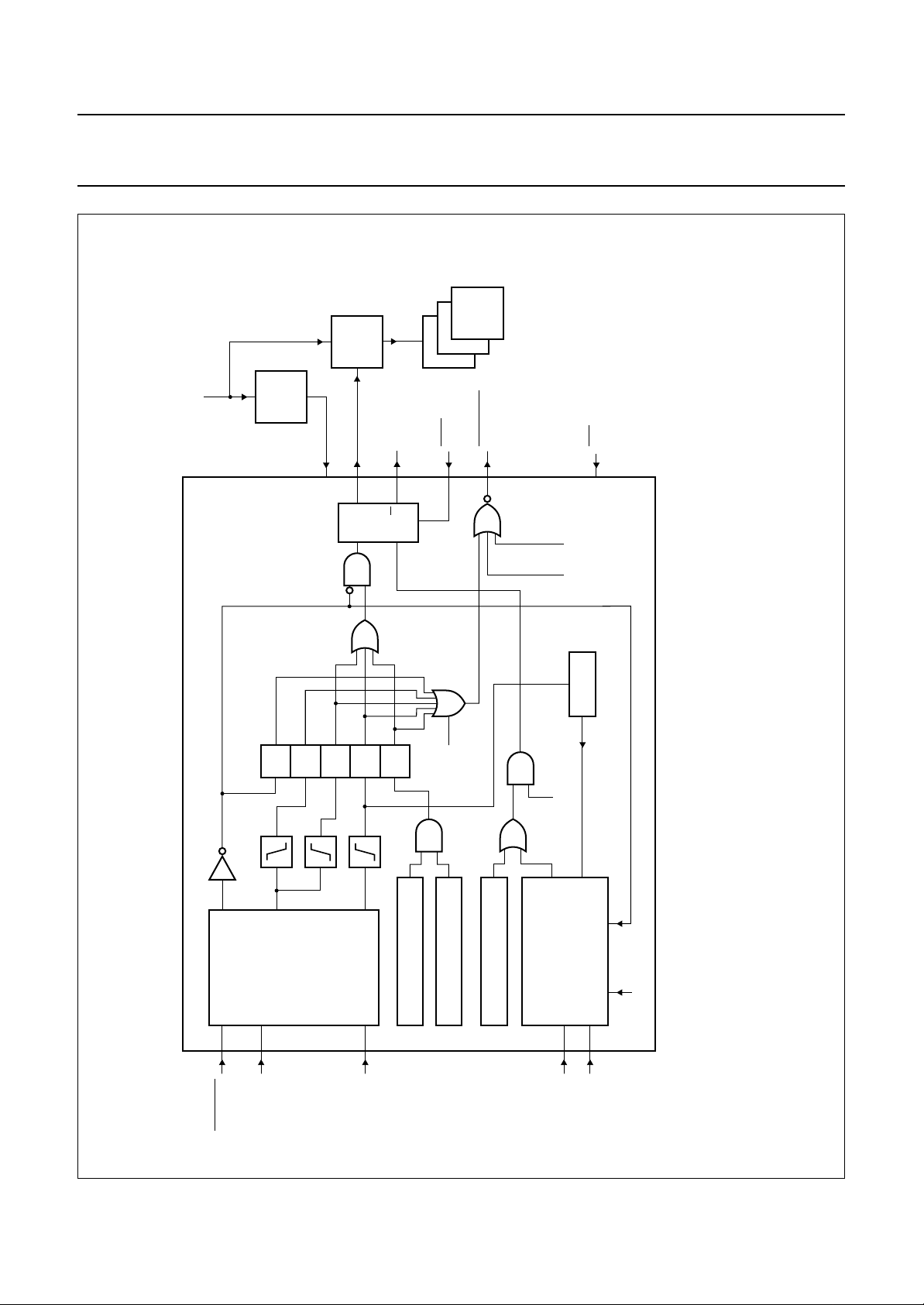
8.2 ON/OFF Logic
The ON/OFF logic performs the main power on and off
switching function for the whole mobile. The on/off
conditions are controlled via an operators keyboard, a low
voltage battery indication circuit, a hardware Watchdog
Timer or an auxiliary switch on input for general purpose
use.
The hardware control interrupt HWCTRL_INT, signalled
via the COMB_INT output (refer to Section 10.2), is used
to signal the status of the ON/OFF Logic. The inputs
DSPEN and TIMEN are used to control the Watchdog
function.
The inputs ONKEY, AUXON and LOWVOLT are
debounced with a time constant of 62.5 ms. The minimum
pulse width for the safe detection of a signal transition is
therefore 2 × 62.5 = 125 ms on any of these lines. The
ON/OFF Logic signals are specified in Table 4.
Table 4 ON/OFF Logic signals
ONKEY Input (active HIGH) to be connected to the
AUXON Input (edge sensitive) for general purpose
LOWVOLT Input (active LOW) to be connected to an
POWON Output (active HIGH) to be connected to
NPOWON Inverted output signal of POWON.
RST and RSTO are asynchronous reset lines.
SIGNAL DESCRIPTION
ON/OFF switch of the operators keyboard.
use, e.g. used as battery charger connect
indication or ignition sense in mobile
applications.
external low battery indication circuit.
the ON terminal of the supply voltage
switch.
8.2.1 MOBILE SWITCH-ON PROCEDURE Switching on the mobile is initiated via the PCF5083
according to Table 5.
If one of the three conditions ONKEY, AUXON or Alarm
time match become true, a corresponding flag is set in
register HWCTRL_REG. As soon as one of these flags is
set, signal POWON is set and NPOWON is reset. At the
same time the HWCTRL_INT interrupt is activated. The
interrupt condition is signalled via the COMB_INT line to
the System Controller if the relevant bit is set in the
COMBINT_REG register (refer to Section 10.2).
The hardware reset
COMB_INT interrupt lines.
The interrupt flags in register HWCTRL_REG must be
cleared by the System Controller to deactivate the
interrupt condition. A flag is cleared by writing a logic 1 to
its bit location.
The POWON output is the main power control signal. As
soon as POWON goes HIGH, all ICs in the mobile are
powered via the supply voltage switch. The LOWVOLT
input asserted LOW, indicating a low voltage situation, or
RSTO asserted LOW inhibits the mobile to be switched on.
If the PCF5083 was switched on via AUXON
(HWCTRL_REG[AUXON_LH] = 1) and the AUXON signal
remains HIGH, the flag HWCTRL_REG[AUXON_LH] must
be cleared, before the PCF5083 enters the Power-down
mode.
RST clears the enable bits for the
Table 5 Mobile switch-on conditions
RST0 LOWVOLT ONKEY AUXON
L X X X X L 3-state
H L X X X L 3-state
HHL→HX X L→HH→L
HH XL→HX L→HH→L
H H X X yes L → HH→L
1996 Oct 29 17
ALARM TIME MATCHES
CURRENT TIME
POWON COMB_INT
Philips Semiconductors Objective specification
GSM signal processing IC PCF5083
8.2.2 MOBILE SWITCH-OFF PROCEDURE The switch-off request to the System Controller is initiated
via a LOW-to-HIGH transition and hold of pin ONKEY for
longer than 1 second or a LOW level on pin LOWVOLT.
The HWCTRL_INT interrupt is activated if one of these
conditions has set it’s corresponding flag in register
HWCTRL_REG.
The next step is to deactivate the POWON signal.
Therefore the flag HWCTRL_REG[SWOFF] has to be set.
If the SWOFF flag is not set within 8 seconds (see
Section 8.2.3) and the Watchdog Timer expires, POWON
is deactivated without any further interaction. The SWOFF
flag is automatically cleared when the mobile is switched
on again.
The PCF5083 is immediately and under all conditions
forced into the off state with
Table 6 Mobile switch-off request conditions
ONKEY
HH H
L→HX H→L
XH→LH→L
LOWVOLT COMB_INT
RSTO asserted LOW.
It should be noted that:
• If POWON is LOW (switch-off state), all outputs of the
PCF5083 except POWON and NPOWON are in their
high-impedance state.
• The hardware control interrupt (HWCTRL_INT) is not
asserted externally but stays internally pending during
Sleep mode. The timing generator unit is forced into
wake-up state if the hardware control interrupt is
asserted internally.
• Other interrupt conditions, caused by the MMI
power-down unit and the real time clock unit, are also
indicated with the hardware control interrupt. These
conditions are mentioned in the appropriate sections.
• The interrupt flags in register HWCTRL_REG have to be
cleared by the System Controller to deactivate the
interrupt condition. A flag is cleared by writing a logic 1
to its bit location.
Table 7 Mobile switch-off conditions
HWCTRL_REG[SWOFF] OFF/WATCHDOG TIMER EXPIRES
LnoHH
L→HnoHH→L
L yes H H → L
XXLH→L
RSTO POWON
1996 Oct 29 18
Philips Semiconductors Objective specification
GSM signal processing IC PCF5083
VOLTAGE
supply
voltage
REGULATORS
IN
V
V
OUT
IN
OUT
V
V
ON
ICs IN MOBILE
full pagewidth
3
bits
HWCTRL_REG
POWON
Q
S
NPOWON
Q
MR
R
RSTO
COMB_INT
RST
MGE288
other
interrupts
HWCTRL_INT
1
0
2
5
other
sources
≥ 1 sec
T
POWON
Fig.7 ON/OFF logic functional diagram.
ALARM TIME
CURRENT TIME
ONKEY
AUXON
LOWVOLT
T = 62.5 ms
DEBOUNCING
1996 Oct 29 19
Wtg/OFF mode
TIMER EXPIRY
HWCTRL[SWOFF] = 1
8 sec WATCHDOG/OFF
enable
TIMEN
DSPEN
enable retrigger
retrigger
read HWCTRL_REG

Philips Semiconductors Objective specification
GSM signal processing IC PCF5083
8.2.3 OFF TIMER AND WATCHDOG TIMER The hardware switch-off and Watchdog Timer are used to
power-down the mobile if the System Controller has lost
control for more than 8 seconds.
8.2.3.1 Watchdog Timer
After the reset signal RST is deactivated, the Watchdog
Timer starts to count. If the timer expires after 8 seconds,
the POWON output is set LOW. To prevent this occurring,
the System Controller must restart the timer periodically,
reading register HWCTRL_REG within 8 seconds after the
previous read operation. The Watchdog function is
enabled if DSPEN = TIMEN = LOW. The configuration
DSPEN = TIMEN = HIGH disables the Watchdog Timer.
All other settings are for debugging purposes.
8.2.3.2 OFF Timer
After the switch-off request (HWCTRL_INT activated via
LOWVOLT or ONKEY conditions), the OFF-Timer starts to
count. If the timer expires after 8 seconds, or if the System
Controller sets HWCTRL_REG[SWOFF] to a logic 1, the
POWON output is set LOW. The OFF-Timer cannot be
restarted with a read access to register HWCTRL_REG.
For some special purposes, e.g. if the battery charging
control is handled from the System Controller, the
OFF-Timer can be stopped after it was activated from
ONKEY or LOWVOLT. It then resumes its watchdog
function. The OFF-Timer is stopped with a write access to
register STOP_REG. The data value written to this register
has to be A5H. Other data values do not stop the
OFF-Timer.
It should be noted that:
• The OFF/Watchdog Timer is not restarted after a stop
operation
• If either the ONKEY or LOWVOLT line stays active after
a stop operation, it is again recognized after its 1 second
switch-off time-out or 62.5 ms debouncing period,
respectively.
8.3 Timing Generator
The Timing Generator provides TDMA timing and
power-down signals for the RF transmitter, RF receiver,
synthesizer and baseband interface IC.
The Timing Generator has three modes of operation to
control the mobile:
1. Normal mode: in this mode the mobile is fully active.
All ICs receive their operating voltage, the power
consumption is reduced by switching the ICs on and
off with their power-down inputs.
2. Sleep or Idle mode: in this mode the mobile is
switched on, but no call is active. The mobile will be
fully activated if a mobile originated call is requested
via the keyboard. Otherwise parts of the mobile are
activated from time to time to monitor incoming calls.
Outside these intervals all ICs can be switched off
under control of the PCF5083. In this mode the main
13 MHz clock is switched off. To maintain TDMA
timing alignment, the PCF5083 is running temporarily
on a slower clock frequency.
3. Reduced Sleep mode: this mode is equal to the
Sleep mode, except that the TDMA timing alignment is
maintained by the main 13 MHz clock.
In this chapter the following definitions are used:
• 1 bit (Bit) = 48 × s = 3.692 µs ( TDMA
frame)
• 1 quarterbit (QB) =
frame)
• 1 timeslot (TS) = 625 QB = 0.576 ms (
• 1 Burst = 1 TS
The term frame refers to a TDMA frame throughout this
section unless otherwise stated.
The Timing Generator consists of:
• The quarterbit counter (QBC) counting 5000 quarterbit
steps in one TDMA frame and running on 1.0833 MHz.
This clock is switched off during Sleep mode.
• The Timing Generator (TG) with output polarity and
mask registers.
• The sleep quarterbit counter (SQBC).
• The Sleep mode timing generator.
1
-------------------------13000000
1
⁄4Bit = 0.923 µs ( TDMA
1
------------ 1250
1
------------ 5000
1
⁄8TDMA frame)
1996 Oct 29 20
Philips Semiconductors Objective specification
GSM signal processing IC PCF5083
8.3.1 THE QUARTERBIT COUNTER The quarterbit counter (QBC) represents the timebase of
the mobile. It consists of a 13-bit upcounter. The counter
directly counts the quarterbit steps within one TDMA
frame. Its range is therefore 0 to 4999.
At the beginning of every TDMA frame (quarterbit counter
state 0) the signal FRAME_INT goes LOW, generating an
interrupt (frame interrupt) to the System Controller. The
interrupt line is deactivated by accessing the register
MODE0_REG. The frame interrupt is disabled with
MODEx_REG[DISFRAMEINT] = 1.
8.3.1.1 Initial Quarterbit Counter Timing Alignment
The timing offset between a base station and a mobile
station can be corrected by presetting the quarterbit
counter with an estimated correction value. Therefore the
register QBC_REG has to be set up with this correction
value in frame N and the flag QBRCTRL_REG[SYNC] has
to be set.
At the end of frame N the quarterbit counter is loaded from
QBC_REG with zeros. The duration of frame N + 1 is
5000 − [QBC_REG] and the mobile will be synchronised at
the beginning of frame N + 2. The frame interrupt at the
beginning of frame N + 1 is disabled. The timing
generation is disabled during frame N + 1. The SYNC flag
is cleared after synchronization.
For the System Controller the resulting timing looks like
frame N being extended and synchronization being
achieved with frame N + 1.
8.3.1.2 Maintaining the Quarterbit Counter Timing
Alignment
Small timing corrections can be made by inserting or
extracting one quarterbit step at the beginning of a TDMA
frame. Therefore the INSERT or EXTRACT flag in register
QBCCTRL_REG have to be set. These flags are cleared
after the timing alignment was performed.
The output polarity can be changed by setting the
corresponding bit in register POL_REG to a logic 1. The
signals can be clamped to a level depending on their flag
in POL_REG by setting the corresponding bit in register
MASK_REG to a logic 0.
After a reset with
synthesizer control lines are set to their inactive level.
The general MS timing is assumed to have the receive
timeslot (RX) in timeslot 0, the transmit timeslot (TX) in
timeslot 3 and the monitor timeslot (MON) in timeslot 6
within a TDMA frame.
Table 8 Output signals
SIGNAL DESCRIPTION
Signals for the receiver section
RXON baseband interface IC receiver enable
BEN baseband interface IC enable
PDRX1 receiver power-down 1
PDRX2 receiver power-down 2
Signals for the transmitter section
TXON baseband interface IC transmitter enable
BEN baseband interface IC enable
TXKEY1 power amplifier power-down
TXKEY2 power ramping controller trigger signal
PDTX1 transmitter power-down 1
NPDTX1 inverted output of PDTX1
NPDTX2 transmitter power-down 2
PDPIAS power amplifier bias voltage power-down
NPDBIAS inverted output of PDBIAS
Signal for the synthesizer
PDSYN synthesizer power-down
RST, the receiver, transmitter and
8.3.2 N
In Normal mode the Timing Generator provides the output
signals specified in Table 8.
The power-down signals NPDTX2, NPDTX1 and
NPDBIAS are active LOW by default. All other signals are
active HIGH by default. Active HIGH in this context means
that the signals are on high level during a receive or a
transmit burst.
1996 Oct 29 21
ORMAL MODE
Philips Semiconductors Objective specification
GSM signal processing IC PCF5083
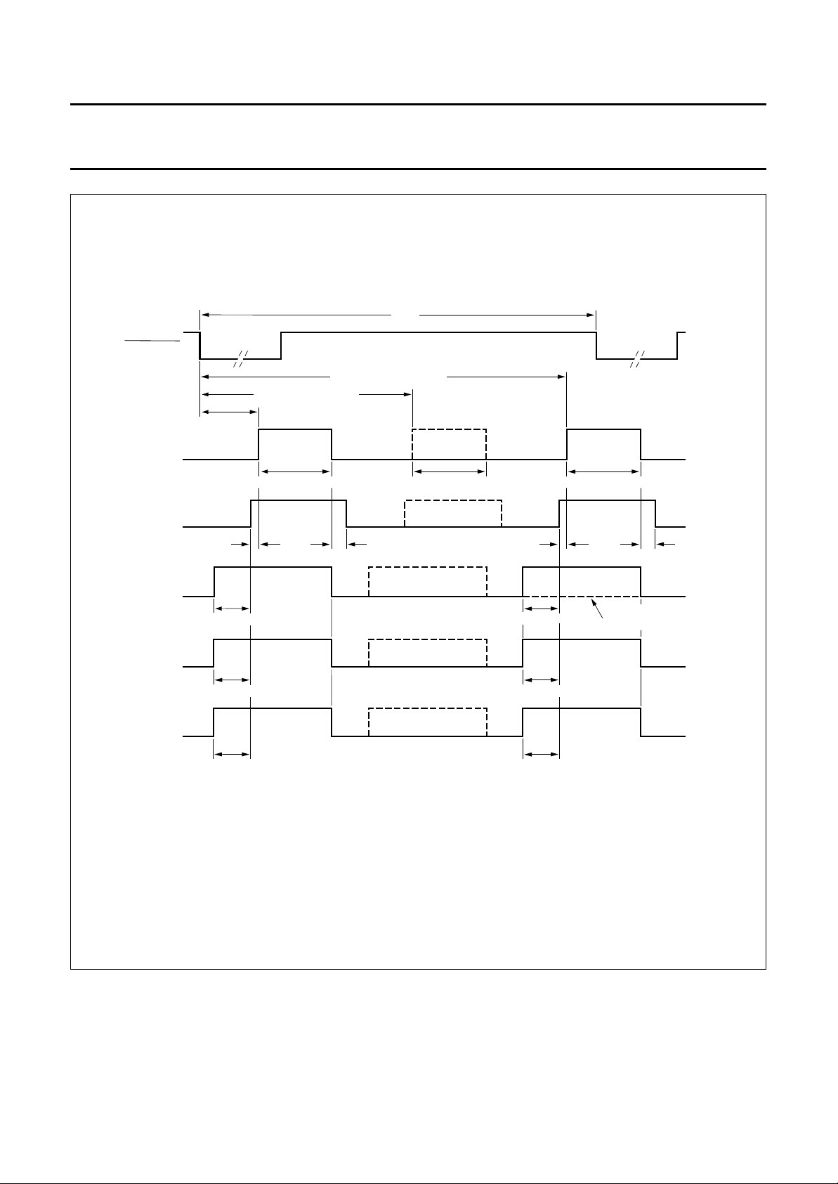
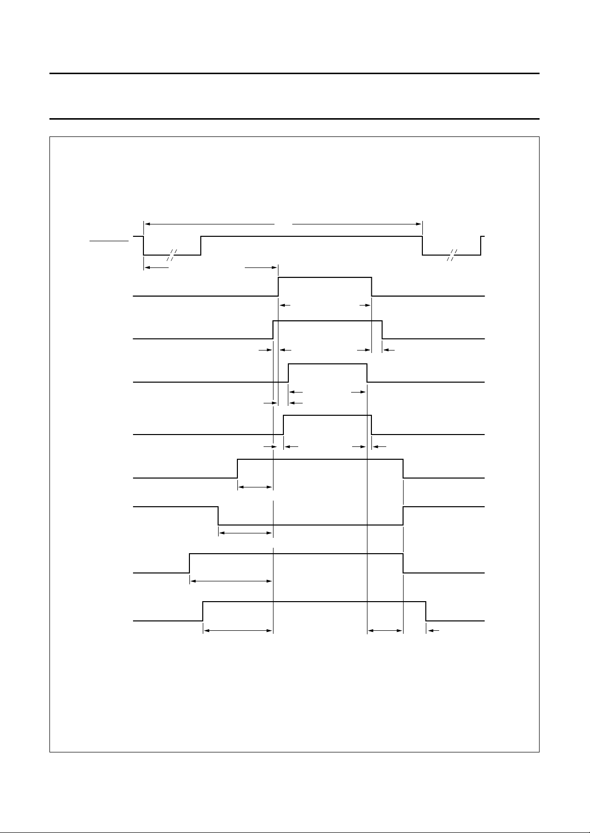
8.3.2.1 Receiver Timing
The Receiver Timing is characterized in Table 9. The start and duration times are defined by loading the mentioned
registers.
Table 9 Receiver Timing (note 1)
BURST TYPE
SIGNAL
Rx burst
START (QB)
(3)(4)
(2)
DURATION (BIT)
RXON RXSTART_REG + 929 = (0 to 127) + 929 RXLENGTHx_REG = (1 to 255)
BEN RXSTART_REG + 928 = (0 to 127) + 928 RXLENGTHx_REG +4=(1to255) + 4
PDRX1
(5)
RXSTART_REG + 1024 − PDRX1_REG × 32 =
to end of RXON
(0 to 127) + 1024 − (0 to 31) × 32
PDRX2 RXSTART_REG + 1024 − PDRX2_REG × 32 =
to end of RXON
(0 to 127) + 1024 − (0 to 31) × 32
PDSYN RXSTART_REG + 1024 − PDSYN_REG × 32 =
to end of RXON
(0 to 127) + 1024 − (0 to 31) × 32
MON burst
(6)(7)(8)
RXON MONSTART_REG + 929 = (0 to 4999) + 929 RXLENGTHx_REG = (1 to 255)
BEN MONSTART_REG + 928 = (0 to 4999) + 928 RXLENGTHx_REG +4=(1to255) + 4
PDRX1
(5)
MONSTART_REG + 1024 − PDRX1_REG × 32 =
to end of RXON
(0 to 4999) + 1024 − (0 to 31) × 32
PDRX2 MONSTART_REG + 1024 − PDRX2_REG × 32 =
to end of RXON
(0 to 4999) + 1024 − (0 to 31) × 32
PDSYN MONSTART_REG + 1024 − PDSYN_REG × 32 =
to end of RXON
(0 to 4999) + 1024 − (0 to 31) × 32
Notes
1. A minimum delay of 948 quarterbit periods must be programmed between the end of a monitor burst and the start of
the next monitor burst, measured from the falling edge of RXON to the next rising edge of RXON.
2. If (MONSTART_REG + 929) > 5000 then the monitor burst ends in the next TDMA timeslot at (MONSTART_REG
+ 929) − 5000.
3. MODEx_REG[RECRX] enable the generation of Rx burst timing.
4. RXBURSTx_REG (x = 0 to 2) is selected with 2 flags in register MODEx_REG.
5. PDRX1 is not activated during a monitor burst if the MODEx_REG[RXCAL] flag is set.
6. For the three level measurement mode, a second monitor burst can be generated during the TX timeslot. The start
position of this burst is then controlled with register TXSTART_REG. Its duration is given from the same register as
for the actual monitor burst.
7. If (MONSTART_REG + 929 +RXBURSTx_REG) > 5000 then the monitor burst ends in the next TDMA timeslot at
(MONSTART_REG + 929 + RXBURSTx_REG) − 5000.
8. MODEx_REG[RECMON] enable/disable the generation of monitor burst timing.
1996 Oct 29 22
Philips Semiconductors Objective specification
GSM signal processing IC PCF5083
handbook, full pagewidth
FRAME_INT
RXON
BEN
PDRX1
PDRX2
TXSTART_REG + 929
RXSTART_REG + 929
RXBURSTx_REG × 4
1
(PDRX1_REG − 3) × 32
(PDRX2_REG − 3) × 32
5000
MONSTART_REG + 929
RX (TX) MON
MONBURSTx_REG × 4
16 1
(PDRX1_REG − 3) × 32
3rd level measurement
(PDRX2_REG − 3) × 32
MONBURSTx_REG × 4
16
RX calibration
timing
PDSYN
(PDSYN_REG − 3) × 32
Fig.8 Receiver timing.
1996 Oct 29 23
(PDSYN_REG − 3) × 32
MGE290

Philips Semiconductors Objective specification
GSM signal processing IC PCF5083
8.3.2.2 Transmitter Timing
The transmitter timing is shown in Table 10. The start and duration times are defined by loading the named registers.
Table 10 Transmitter Timing
BURST TYPE
SIGNAL
TX burst
TXON TXSTART_REG + 929 = (0 to 2047) + 929 TXLENGTHx_REG = (1 to 255)
BEN TXSTART_REG + 928 = (0 to 2047) + 928 to end of TXON + 16
(N)PDTX1,2 TXSTART_REG + 1024 − PDRX1,2_REG × 32 =
(0 to 2047) + 1024 − (0 to 31) × 32
(N)PDBIAS TXSTART_REG + 1024 − PDBIAS_REG × 32 =
(0 to 2047) + 1024 − (0 to 31) × 32
or if PDBIAS_REG < PDTX1_REG + 4 (note 3):
TXSTART_REG + 1024 − (PDTX1_REG + 4) × 32
= (0 to 2047) + 1024 − (0 to 31) × 32
TXKEY1 TXSTART_REG + 929 + KEYON1_REG =
(0 to 2047) + 929 + (1 to 511) × 32
TXKEY2 TXSTART_REG + 929 + KEYON2_REG =
(0 to 2047) + 929 + (1 to 511) × 32
PDSYN TXSTART_REG + 1024 − PDSYN_REG × 32 =
(0 to 2047) + 1024 − (1 to 31) × 32
Notes
1. The timing advance is adjusted with the value of TXSTART_REG.
2. TXBURSTx_REG and TXKEYx_REG (x = 0 or 1) is selected with a flag in register MODEx_REG.
3. Therefore (N)PDBIAS will always be active at least 4 × 32 QB prior to PDTX1.
START (QB)
(1)
DURATION (QB)
to end of TXKEY + PDDELAY_REG
(1 to 63)
to end of
TXKEY + PDDELAY_REG + 32 (1 to 63)
TXKEYx_REG = (1 to 1023)
to end of TXKEYx + KEYOFF_REG
(1 to 63)
to end of TXKEYx + PDDELAY_REG
(1 to 63)
(2)
1996 Oct 29 24
Philips Semiconductors Objective specification
GSM signal processing IC PCF5083
handbook, full pagewidth
FRAME_INT
TXON
BEN
TXKEY1
TXKEY2
PDTX1
5000
TXSTART_REG + 929
TXBURSTx_REG × 4
116
TXKEYx_REG
KEYON1_REG
KEYON2_REG KEYOFF_REG
(PDTX1_REG − 3) × 32
NPDTX2
(PDTX2_REG − 3) × 32
PDSYN
(PDSYN_REG − 3) × 32
PDBIAS
(PDBIAS_REG − 3) × 32
or
(PDTX1_REG + 1) × 32
(see text)
Fig.9 Transmit burst timing.
1996 Oct 29 25
PDDELAY_REG
32
MGE291
Philips Semiconductors Objective specification
GSM signal processing IC PCF5083
8.3.2.3 Timing Generation
To generate all burst types required to fulfil the GSM timing, it is necessary to combine and/or modify the basic receive
and transmit burst sequences. For this purpose two registers MODE0_REG and MODE1_REG exist, containing some
flags to control the burst timing. Both mode registers and the registers RXSTART_REG, TXSTART_REG and
MONSTART_REG have an additional pipeline stage.The first register stage can be read or written by the SC.
The second stage is used for timing generation. The pipelining operation is performed at QBC = 0 (together with the
frame interrupt generation). Some flags inside the mode registers have a third pipelining stage to allow the generation of
a MON burst which overlaps into the next frame. The System Controller must set up the registers within the frame before
the programmed timing becomes active. Which register MODE0_REG or MODE1_REG is actually used is described in
Table 11. MODE0_REG and MODE1_REG contain identical flags.
Table 11 Mode Registers (MODE0_REG and MODE1_REG)
BIT FLAG DESCRIPTION
13 USEMODE MODE_REGx select. If USERMODE = 0; then switch to MODE_REG0 after the next
frame. If USERMODE = 1; then switch to MODE_REG1 after the next frame.
12 DISFRAMENT Disable frame interrupt. If DISFRAMENT = 1; then the frame interrupt is disabled.
11 RXCAL RX calibration timing. If RXCAL = 1; then the RX calibration timing is generated.
10 TXLENGTH Register select. The state of this bit determines which registers are used for the TX
burst. If TXLENGTH = 0; then registers TXBURST0_REG and TXKEY0_REG are
used. If TXLENGTH = 1; then registers TXBURST1_REG and TXKEY1_REG are
used.
9 MONLENGTH1 RXBURSTx_REG select. The state of these two bits determine which RXBURST
8 MONLENGTH0
7 RXLENGTH1 RXBURSTx_REG select. The state of these two bits determine which RXBURST
6 RXLENGTH0
5 DTX DTX timing enable. If DTX = 1; then DTX timing is enabled.
4 SEND TX burst timing. If SEND = 1; the TX burst timing is generated.
3 RECON Receiver start-up. If RECON = 1, the receiver start-up sequence for the MON burst
2 RECMON MON burst timing. If RECMON = 1; the MON burst timing is generated.
1 RECTX Third level measurement. If RECTX = 1; then the MON burst timing during the TX
0 RECRX Rx burst timing. If RECRX = 1; the Rx burst timing is generated.
register is used for the MON burst; see Table 12.
register is used for the Rx burst; see Table 13.
in the idle frame is generated.
timeslot for a third level measurements generated.
Table 12 Register selection for the MON burst
MONLENGTH1 MONLENGTH0 REGISTER SELECTED
0 0 RXBURST0_REG is used.
0 1 RXBURST1_REG is used.
1 0 RXBURST2_REG is used.
1 1 Undefined during a MON burst.
1996 Oct 29 26

Philips Semiconductors Objective specification
GSM signal processing IC PCF5083
Table 13 Register selection for the Rx burst
RXLENGTH1 RXLENGTH0 REGISTER SELECTED
0 0 RXBURST0_REG is used.
0 1 RXBURST1_REG is used.
1 0 RXBURST2_REG is used.
1 1 Undefined during a RX burst.
8.3.2.4 MON burst during idle frame
This burst is a special case of the MON burst. It is used for FCB search and for monitoring during the idle frame. If
RECON is set, a timing equivalent to the MON burst timing is generated, with the exception that all output lines (BEN,
RXON, PDRXx etc.) are kept active at the end of the burst. The output lines are set inactive again during the first frame
with RECMON set at the time, they normally would be deactivated at the end of a MON burst. During the frames in
between, either RECON = 1, or RECRX = RECTX = RECMON = RECON = SEND = 0 must be programmed.
8.3.2.5 Register mode switching
Which of the registers MODE0_REG or MODE1_REG is used for timing generation is determined using the following two
rules:
1. After any write access to MODE0_REG, MODE0_REG is active during the next frame.
2. After every frame the USEMODE flag of the currently active register determines which register is used during the
next frame, unless there was a write access to MODE0_REG during the current frame.
e.g. MODE0_REG: USEMODE = 1 and MODE1_REG: USEMODE = 0 is programmed during frame N.
This causes the following timing:
a) MODE0_REG is active during frame N + 1
b) MODE1_REG is active during frame N + 2
c) MODE0_REG is active during frame N + 3 and so on, until MODE0_REG is being written again.
8.3.2.6 DTX Mode Processing
DTX mode (Discontinuous Transmission) is enabled with MODEx_REG[DTX] = 1. In DTX mode, the DSP makes the
decision whether a TX burst should be generated or not. The DTX condition is signalled via IO4 (generate transmit burst:
IO4 = 0, no transmit burst: IO4 = 1). If no TX burst is to be generated, the power-down lines TXKEY1/2, (N)PDTX1/2 and
PDSYN are kept inactive or if already asserted, they are set inactive again. (N)PDBIAS become inactive with their default
delay of 8 bit after (N)PDTX1/2 respective PDSYN if they were already asserted, otherwise they also remain inactive.
TXON and BEN are not affected from DTX mode.
8.3.2.7 Interface to the RF-IC Bus
The Timing Generator provides trigger signals for the frequency and gain control channels of the RF-IC interface when
the quarterbit counter matches either RXSTART_REG, TXSTART_REG or MONSTART_REG. Further trigger signals
are generated for the gain control channel after every receive burst to send the contents of register DACOFF_REG and
prior to a receive burst if the quarterbit counter matches xxSTART_REG + 1024 − AGCSTART_REG × 32 (xx = RX, TX
or MON) to send the contents of register DACON_REG (refer to Section 8.4).
Note, if the generation of a trigger signal falls into an active burst, the trigger signal is delayed until the end of the current
burst.
1996 Oct 29 27

Philips Semiconductors Objective specification
GSM signal processing IC PCF5083
8.3.2.8 Timing modes Application Examples
Table 14 Timing mode applications
FRAME
N 0 1 0 0 0 Receiver on at the start of timeslot 0
N + 1 to N + M 0 0 0 0 0 Keep receiver on.
N + 1 + M 0 0 1 0 0 Receiver off after number of samples defined
X 0 0 0 0 1 Receive during TS0.
X 1 0 1 0 1 Receive during RX, MON, transmit during TX.
I-1 1 1 0 0 1 Receive during RX, transmit during TX, receiver
I 0 0 1 0 0 Receiver off defined by MONSTART_REG and
I-1
(1)
or
I-1 1 0 0 0 1 Receive during RX, transmit during TX.
I
(1)
or
I 0 0 1 0 0 Receive during MON.
X 0 0 1 1 1 Receive during RX, TX and MON slot.
X 1 0 0 0 0 Transmit during TX.
43 2 10
SEND RECON RECMON RECTX RECRX ACTION
BCCH Detection
(MONSTART_REG = 0) in TDMA frame N + 1.
Receiver on.
by MONSTART_REG, RXLENGTHx_REG and
number of TDMA frames M.
Frequency Estimation
Frame with RX, TX, MON
Frame before idle frame (monitoring)
on defined by MONSTART_REG.
Idle frame (monitoring)
RXLENGTHx_REG.
Frame with RX, TX, MON
1 0 1 0 1 Receive during RX, MON, transmit during T.
Idle frame (SYNC burst reading)
0 0 0 0 0 No operation.
Three level measurements
Send access burst
BIT ASSIGNMENT;
REGISTER MODE_REG
Note
1. The SYNC burst location is defined by MONSTART_REG. If a timing is required with s = MONSTART_REG ≥ 5000,
MONSTART_REG is programmed with s mod 5000 and the second alternative is used.
1996 Oct 29 28
Philips Semiconductors Objective specification
GSM signal processing IC PCF5083
During the three level measurement mode the burst length
of the receive burst during the TX slot is defined by the
same register RXBURSTx_REG as used for the
MON burst. The receive frequency must be set by
programming the TX channel of the RF_IC interface.
For a certain operation mode in frame N, the Timing
Generator has to be programmed with all necessary
parameters in frame N − 1. For this purpose the registers
RXSTART_REG, TXSTART_REG, MONSTART_REG
and MODEx_REG have an additional pipelining stage.
The pipelining takes place at the beginning of every TDMA
frame with the frame interrupt generation.
8.3.3 S
The Sleep mode circuitry is used to reduce the power
consumption during the Idle mode. During Sleep mode,
the mobile is switched on, but no call is active. The mobile
is only activated to read the paging blocks and for
neighbour cell monitoring. Outside these intervals, all ICs
can be switched off to save power.
Table 15 Signals controlled by the PCF5083 during Sleep mode
REFON Reference oscillator on. Active HIGH output.
NREFON Inverted REFON output.
DSPON DSP power-down (connected on chip).
GPON1 General purpose power-down and radio part interface 3-state enable. Active HIGH output.
GPON2 General purpose power-down. Active HIGH output.
LEEP MODE
SIGNAL DESCRIPTION
In this mode also the main 13 MHz oscillator may be
switched off. To maintain TDMA timing alignment, the
PCF5083 is running temporarily on a slower clock
frequency, derived from the 32.768 kHz real time clock
oscillator. This clock is called Sleep Clock (SLCLK).
During the Sleep mode the PCF5083 controls the signals
specified in Table 15, the timing for these signals is
detailed in Table 16.
Sleep mode is activated with
QBCCTRL_REG[SLEEP] = 1 and
QBCCTRL_REG[SLEEPRED] = 0 (the SLEEPRED flag is
used for reduced Sleep mode, see below). The register
SLEEPCNT_REG has to be programmed with the number
of TDMA frames the mobile wants to sleep minus one.
Register FRAMECNT_REG is automatically cleared when
the Sleep mode is entered and counts the number of
TDMA frames actually slept. The 9-bit registers
SLEEPCNT_REG and FRAMECNT_REG allow a
maximum Sleep mode period of 512 frames. Refer to
Fig.11 for the signal flow.
Table 16 Sleep mode signal timing
SIGNAL FRAME NUMBER
(N)REFON In frame N + 1 on the third positive SLCLK edge REFON_REG (notes 1 and 2)
DSPON In frame N + 1 on the second positive SLCLK edge KISSON_REG (note 2)
GPON1 In frame N + 1 on the second positive SLCLK edge GPON1_REG (note 2)
GPON2 In frame N + 1 on the third positive SLCLK edge GPON2_REG (note 2)
Notes
1. (N)REFON is not deactivated if the Sleep mode is initiated while the sleep clock calibration procedure is running (see
Section 8.3.3.3), while the IOM
indicating that the MMI controller requires the 13 MHz clock.
2. Maximum 295 ms before Sleep mode terminates with 4.6 ms resolution {[(0 to 63) + 1] × 4.6 ms}.
1996 Oct 29 29
®
-2 interface is enabled or the MMICLK flag in register HWCTRL_REG is set,
ACTIVATION OF SIGNAL IF
SLEEPCNT_REG EQUALS
Philips Semiconductors Objective specification
GSM signal processing IC PCF5083
A power-down line is only deactivated during Sleep mode
if the corresponding activation register is programmed with
a higher value than register SLEEPCNT_REG. Otherwise
the power-down line stays active during Sleep mode. The
output polarity of the power-down lines can be changed by
setting their corresponding bit in register POL_REG to a
logic 1. The signals can be clamped to a level depending
on their flag in POL_REG by setting the corresponding bit
in register MASK_REG to a logic 0.
Because the 13 MHz clock is also internally disabled
during Sleep mode, the PCF5083 cannot be accessed
with the host port.
During Sleep mode, burst timing and frame interrupt
generation is stopped and the registers MODE0_REG and
MODE1_REG are cleared.
8.3.3.1 Transceiver control lines
The timing generator signals RXON, TXON, BEN, PDRX1,
PDRX2, PDTX1, NPDTX1, NPDTX2, PDBIAS, NPDBIAS,
PDSYN, TXKEY1, TXKEY2 and the RF device control bus
signals RFCLK, RFDO, RFEN1 to RFEN4, RFE and the
Voice Port signals ASF, ACLK and ADO are 3-stated as
long as the signal GPON1 is inactive during Sleep mode.
The signals are driven into their high-impedance state
independently of the actual polarity to which GPON1 is
programmed, unless MASK_REG[GPON1] = 0. In this
case the outputs are driven during Sleep mode.
8.3.3.2 The Sleep Quarterbit Counter
In Sleep mode, the 13 MHz reference oscillator is switched
off to reduce the power consumption. The TDMA timing is
maintained using the sleep quarterbit counter (SQBC),
which is driven from the sleep clock (SLCLK). The sleep
clock is derived from the 32.768 kHz real time clock. Upon
entering Sleep mode, the contents of the quarterbit
counter are copied to the sleep quarterbit counter. After
the end of a Sleep mode period, the sleep quarterbit
counter is copied back to the quarterbit counter and normal
timing is performed again.
To maintain the correct timing over hundreds of TDMA
frames, the sleep quarterbit counter is incremented with
the value SQBC_INC equal to the clock ratio between the
quarterbit clock and the sleep clock. This value must be
very accurate and can be derived using the calibration
method described in Section 8.3.3.3.
handbook, full pagewidth
13 MHz
QBCCTRL_REG[SLEEP]
32768 Hz
QBCCTRL_REG[CAL]
÷ 12
EN
EN
÷ 4
1.08325 MHz
Enter sleep mode:
Copy QBC to SQBC
SLCLK
8192 Hz
1083
8.192
(0 to 4999)
SQBC_INC
(0 to 255)
Fig.10 Quarterbit counters for normal and Sleep mode.
1996 Oct 29 30
QBC
SQBC
+
typ. 123
Enter normal mode:
Copy SQBC to QBC
reduced
sleep
mode
TIMING
GENERATOR
NORMAL
MODE
TIMING
GENERATOR
SLEEP
MODE
MGE289
RXON
TXON
BEN
PDRX1,2
(N)PDTX1,2
SYNON
(N)PDBIAS
TXKEY1,2
GPON1
GPON2
DSPON
REFON
NREFON
 Loading...