

Philips PCF5078T-F1, PCF5078T-F2 Datasheet

DATA SH EET
Product specification
File under Integrated Circuits, IC17
1999 Apr 12
INTEGRATED CIRCUITS
PCF5078
Power amplifier controller for GSM
and PCN systems

1999 Apr 12 2
Philips Semiconductors Product specification
Power amplifier controller for GSM and
PCN systems
PCF5078
FEATURES
• Compatible with baseband interface family PCF5073x
• Two power sensor inputs
• Temperature compensation of sensor signal
• Active filter for DAC input
• Power Amplifier (PA) protection against mismatching
• Bias current source for detector diodes
• Generation of pre-bias level for PA at start of burst
(home position)
• Possibility to adapt home position by external
components
• Applicable for a wide range of silicon and GaAs power
amplifiers.
APPLICATIONS
• Global System for Mobile communication (GSM)
• Personal Communications Network (PCN) systems.
GENERAL DESCRIPTION
This CMOS device integrates an amplifier for the detected
RF voltage from the sensor, an integrator and an active
filter to build a PA control loop for cellular systems with a
small amount of passive components.
QUICK REFERENCE DATA
ORDERING INFORMATION
SYMBOL PARAMETER MIN. TYP. MAX. UNIT
V
DD
supply voltage 2.4 3.6 5.0 V
I
DD(tot)
total supply current −−6mA
T
amb
operating ambient temperature −40 − +85 °C
TYPE
NUMBER
PACKAGE
NAME DESCRIPTION VERSION
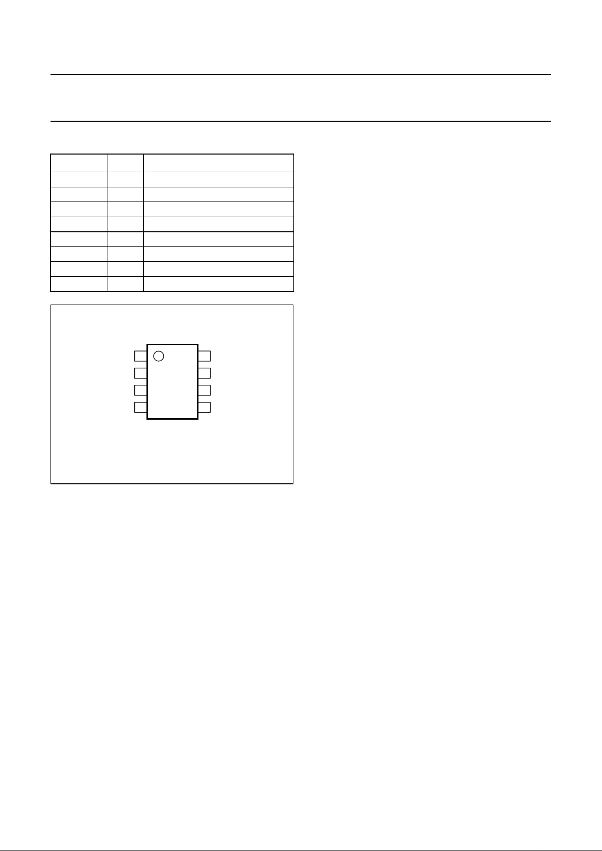
PCF5078T TSSOP8 plastic thin shrink small outline package; 8 leads; body width 3.0 mm SOT505-1
1999 Apr 12 3
Philips Semiconductors Product specification
Power amplifier controller for GSM and
PCN systems
PCF5078
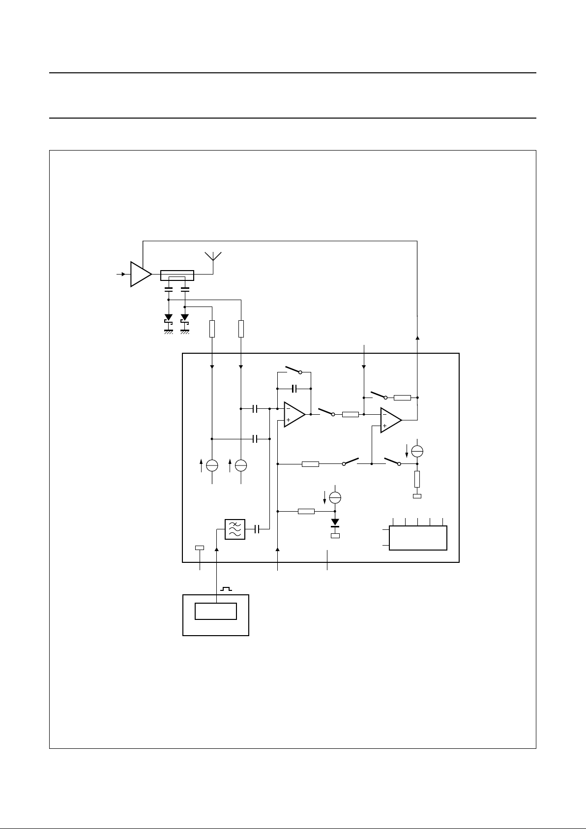
BLOCK DIAGRAM
Fig.1 Block diagram.
MGS193
handbook, full pagewidth
30 µA
10 µA
V
DD
V
DD
10 µA
OP1
OP4
56 7
3421
S1
S1
C1
6 pF
C2
6 pF
C3
5 pF
C4
10 pF
V
DD
VDAC
V
prebias
V
DD
V
home
30 µA
V
DD
8
S2S2S3S3S4S4S5
S5
PCF5078
PCF5073x
50 kΩ
R3
15 kΩ
R6
20 kΩ
R1
1 kΩ
R2
R4
6 kΩ
CONTROL
LOGIC
AUXDAC3
PA
D1 D2
RF
V
DD
VDAC
VINT
VHOME
V
SS
VS2 VS1 VC
sensor
antenna
1999 Apr 12 4
Philips Semiconductors Product specification
Power amplifier controller for GSM and
PCN systems
PCF5078
PINNING
FUNCTIONAL DESCRIPTION
General
The PCF5078 integrates an amplifier for the detected RF
voltage from the sensor, an integrator and an active filter
to build a PA control loop with a small amount of passive
components.
The sensor amplifier is able to amplify signals from a RF
power detector in a range of −20 to +15 dBm. This
complies to the PA output power range of GSM and PCN
systems when a directional coupler with 20 dB attenuation
is used.
The Schottky diode for power detection (sensor) is biased
by an integrated current source of 30 µA. Variations of the
forward voltage of the diodes with the temperature have no
influence on the measured signal, because they are
cancelled by sampling around the switched capacitor
operational amplifier OP1 (see Fig.1).
SYMBOL PIN DESCRIPTION
VC 1 PA control output voltage
VINT 2 negative integrator input
VS1 3 sensor signal input 1
VS2 4 sensor signal input 2
V
SS
5 ground supply
VDAC 6 DAC input voltage
VHOME 7 home position input voltage
V
DD
8 supply voltage
Fig.2 Pin configuration.
handbook, halfpage
1
2
3
4
8
7
6
5
MGS194
PCF5078
V
DD
VDAC
VINT VHOME
V
SS
VS2
VS1
VC
An external Digital-to-Analog Converter (DAC) with10-bit
resolution is necessary to control the loop e.g. the
AUXDAC3 of the baseband interface family PCF5073x.
An integrated active filter smooths the voltage steps of the
DAC and avoids a feedthrough of the DAC harmonics into
the modulation spectra of the PA.
The DAC signal and the sensor signal are added by
operational amplifier OP1. The voltage difference of both
signals is integrated by operational amplifier OP4, which
provides the PA control voltage on pin VC. The integration
is performed by means of an external capacitance C
VINT
connected between pins VINT and VC.
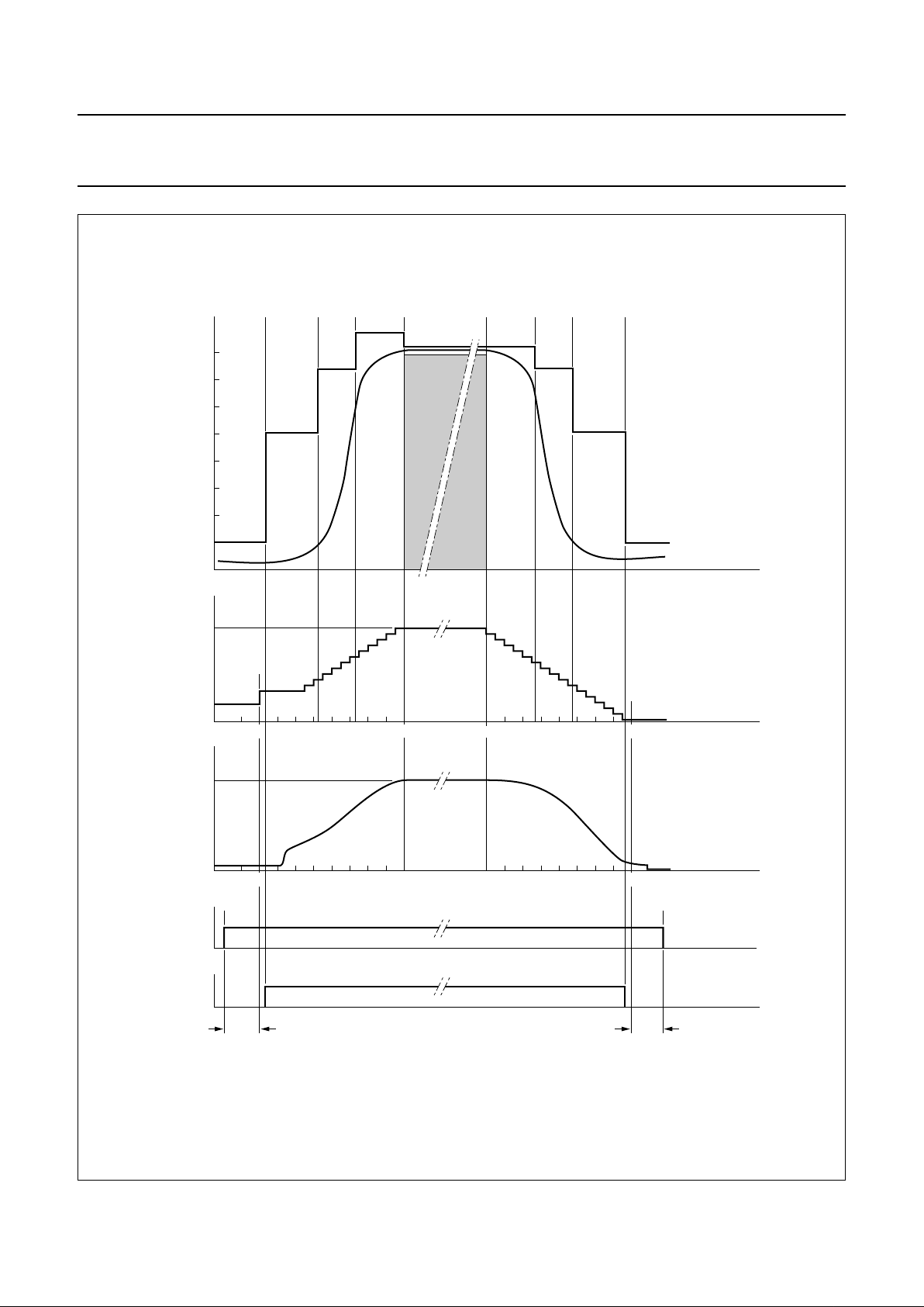
The shape of the rising and falling power burst edges can
be determined by means of the DAC voltage (see Fig.3).
Power-down mode
During the not used time slots in Time Division Multiple
Access (TDMA) systems, the PCF5078 must be turned off
by switching off the supply voltage on pin V
DD
.
Initial conditions and start-up
The PCF5078 has been designed to operate in bursts as
required in TDMA systems. For each time slot to be
transmitted it must be powered-up by switching on the
supply voltage. This allows a proper initialization of
switches S1 to S5.
During start-up switches S1, S2 and S3 are closed and
switches S4 and S5 are opened (see Fig.4).
The forward voltages on the Schottky diodes are sampled
on capacitors C1 and C2, respectively, because switch S1
is closed. Moreover, the control voltage on pin VC is
initially forced to pre-bias level V
prebias
because
switches S2 and S3 are closed and switch S4 is opened.
Switch S1 is opened after a fixed time the supply voltage
has been switched on and then the circuit is ready. This
time is defined on-chip and can be maximum 45 µs. Once
switch S1 is open, a ramp signal with a minimum
amplitude of 25 mV applied on pin VDAC determines
opening of switch S3 and closing of switch S4 with a delay
of maximum 3 µs with respect to the start of the ramp.
After opening switch S3, the control voltage on pin VC
rises in a fixed amount of time to the home position level
so biasing the PA to the beginning of the active range of its
control curve. Switch S2 remains closed during this typical
time of 2 µs. When switch S2 is opened, switch S5 is
closed allowing the transfer of any signal coming from
amplifier OP1.

1999 Apr 12 5
Philips Semiconductors Product specification
Power amplifier controller for GSM and
PCN systems
PCF5078
After this preset, the control voltage is free to increase
according to the control loop if RF input is present
(see Fig.3).
For higher DAC ramp steps the delay time of opening
switch S3 (and closing switch S4) is reduced. On the
contrary, the delay time between opening switch S2 with
respect to opening switch S3 (and closing switch S4)
remains unchanged.
For a correct start-up it is required that the rising time of the
supply voltage is maximum 20 µs.
End of a burst
For a proper down ramp, the final value of the DAC input
voltage should be below the value at the beginning of the
burst and so be able to really shut-off the PA (see Fig.5).
This means the code programmed for the last bit of the
DAC down ramp (CODE
END
) has to be lower than the
initial value of the up ramp (CODE
START
). Moreover, the
last code must be maintained until the supply voltage has
been switched off.
When the voltage on pin VC is detected to be lower than
V
VHOME
a built-in mechanism forces the voltage on pin VC
to V
prebias
by closing switches S1, S2 and S3 and by
opening switches S4 and S5.
For proper operation, the supply voltage should be
switched off at least 15 µs later with respect to the end of
the down ramp on pin VDAC.
PA protection against mismatching
A second sensor amplified input is integrated into the
PCF5078 for measuring the reflected wave of the
directional coupler. The signal is added to the measured
RF power signal (see Fig.3). When mismatching at the
output of the PA occurs the power is reduced. A high
Voltage Standing W ave Ratio (VSWR) at the output of the
PA often occurs in systems where the PA is connected to
the antenna via switches with low attenuation instead of
using a duplex filter.
Home position voltage
A forward voltage of an on-chip silicon diode is provided as
the default home position voltage V
home
. This voltage
matches the requirements at the control input of most PAs
and exhibits the same temperature coefficient.
However, if another value is needed for a certain PA the
level can be adjusted by connecting external components
to pin VHOME (see Figs 10 and 11). The home position
voltage can be set between 200 and 1000 mV when using
a capacitor of 50 pF connected between pins VINT
and VC.
1999 Apr 12 6
Philips Semiconductors Product specification
Power amplifier controller for GSM and
PCN systems
PCF5078
Fig.3 Timing diagram.
MGS197
handbook, full pagewidth
−80
−28 −18 −10 0
1614121086420
+543 +553 +561 +571
−70
−60
<0.9V
DD
V
DD
V
prebias
V
VC
−50
32
DAC bits at 560 kHz
3028262422201816
−40
−30
−20
−10
0
RF
out
(dBc)
time (µs)
time
1614121086420
<0.9V
DD
CODE
START
CODE
END
V
VDAC
32
DAC bits at 560 kHz
3028262422201816
RF
in
time
>15 µs>45 µs
 Loading...