

Philips PCF50732H-F1, PCF50732H-F2 Datasheet

DATA SH EET
Objective specification
File under Integrated Circuits, IC17
1999 May 03
INTEGRATED CIRCUITS
PCF50732
Baseband and audio interface for
GSM

1999 May 03 2
Philips Semiconductors Objective specification
Baseband and audio interface for GSM PCF50732
CONTENTS
1 FEATURES
2 APPLICATIONS
3 GENERAL DESCRIPTION
4 ORDERING INFORMATION
5 QUICK REFERENCE DATA
6 BLOCK DIAGRAM
7 PINNING
8 FUNCTIONAL DESCRIPTION
8.1 General
8.2 Baseband and voice band reference voltages
9 BASEBAND CODEC
9.1 Baseband transmit path
9.2 Baseband receive path
9.3 Baseband Serial Interface (BSI)
10 VOICE BAND CODEC
10.1 Voice band receive path
10.2 Voice band transmit path
10.3 Voice band digital circuitry
11 AUXILIARY FUNCTIONS
11.1 Automatic Gain Control (AGC): AUXDAC1
11.2 Automatic Frequency Control (AFC):
AUXDAC2
11.3 Power ramping: AUXDAC3
11.4 Auxiliary analog-to-digital converter (AUXADC)
12 CONTROL SERIAL INTERFACE (CSI)
12.1 The serial interface
12.2 Control Serial Interface (CSI) timing
characteristics
12.3 Control register block
13 VOICE BAND SIGNAL PROCESSOR (VSP)
13.1 Hardware description
13.2 VSP assembler language
13.3 Descriptions of the VSP instruction set
13.4 The assembler/emulator
14 LIMITING VALUES
15 THERMAL CHARACTERISTICS
16 DC CHARACTERISTICS
17 AC CHARACTERISTICS
18 FUNCTIONAL CHARACTERISTICS
18.1 Baseband transmit (BSI to TXI/Q)
18.2 Baseband receive (RXI/Q to BSI)
18.3 Voice band transmit (microphone to ASI)
18.4 Voice band receive (ASI to earphone)
18.5 Auxiliary digital-to-analog converters
18.6 Auxiliary analog-to-digital converters:
AUXADC1, AUXADC2, AUXADC3 and
AUXADC4
18.7 Typical total current consumption
18.8 Typical output loads
19 APPLICATION INFORMATION
19.1 Wake-up procedure from Sleep mode
19.2 Microphone input connection and test set-up
20 PACKAGE OUTLINES
21 SOLDERING
21.1 Introduction to soldering surface mount
packages
21.2 Reflow soldering
21.3 Wave soldering
21.4 Manual soldering
21.5 Suitability of surface mount IC packages for
wave and reflow soldering methods
22 DEFINITIONS
23 LIFE SUPPORT APPLICATIONS

1999 May 03 3
Philips Semiconductors Objective specification
Baseband and audio interface for GSM PCF50732
1 FEATURES
• Low power and low voltage device in 0.25 micron
CMOS technology; supply voltage: analog 2.7 V
(typical) and digital 1.5 V (typical)
• Compatible with GSM phase 2 and DCS1800
recommendations
• Complete in-phase and quadrature component interface
paths between the Digital Signal Processor (DSP) and
RF circuitry
• Complete linear PCM CODEC for audio signal
conversion between earphone/microphone and DSP
• Four auxiliary analog inputs for measurement purposes
(e.g. battery monitoring)
• Three auxiliary analog outputs for control purposes
(i.e. AFC, AGC and power ramping control)
• Separate baseband, audio and control serial interfaces
• Voice band Signal Processor (VSP) for flexible audio
data processing.
2 APPLICATIONS
The CMOS integrated circuit PCF50732, Baseband and
audio interface for GSM, is dedicated to wireless
telephone handsets conforming to the GSM
recommendations phases 1 and 2, DCS1800 and
PCS1900.
3 GENERAL DESCRIPTION
The baseband CODEC is a complete interface circuit
between the RF part in a mobile communication handset
and the Digital Signal Processor (DSP). It consists of three
parts:
• The receive path, which transforms the quadrature
signals from the RF (I/Q) to digital signals
• The transmit path, which transforms a bitstream to
analog quadrature signals for the RF devices
• The digital Baseband Serial Interface (BSI), which
exchanges baseband data between the PCF50732 and
the digital signal processor. The interface also includes
signals to power-up and power-down the baseband
transmit (TX) and receive (RX) paths.
The voice band CODEC is a complete analog front-end
circuit. It consists of four parts:
• The receive path, which converts a digital signal to an
analog signal for an earpiece, an external loudspeaker
or a buzzer
• The transmit path, which receives the analog external
signal from a microphone and converts it into a digital
signal
• The Voice band Signal Processor (VSP), which filters
the voice band data
• The digital Audio Serial Interface (ASI), which
connects the digital linear PCM signals of the receive
and transmit paths to an external DSP. The voice band
data is coded in 16-bit linear PCM twos complement
words.
The auxiliary Analog-to-Digital Converter (ADC)
section consists of four input channels specified for battery
management applications.
The auxiliary Digital-to-Analog Converter (DAC)
section consists of three DACs for Automatic Gain Control
(AGC), for Automatic Frequency Control (AFC) and for
power ramping.
The Control Serial Interface (CSI) is used to program a
set of control registers, to store the power amplifier
ramping characteristics into the dedicated RAM and to
transmit auxiliary ADC values to the DSP. It also controls
switches, modes and power status of the different parts of
the IC.
4 ORDERING INFORMATION
TYPE NUMBER
PACKAGE
NAME DESCRIPTION VERSION
PCF50732H LQFP48 plastic low profile quad flat package; 48 leads; body 7 × 7 × 1.4 mm SOT313-2
1999 May 03 4
Philips Semiconductors Objective specification
Baseband and audio interface for GSM PCF50732
5 QUICK REFERENCE DATA
Note
1. Without load on audio outputs EARP, EARN, AUXSP and BUZ.
SYMBOL PARAMETER CONDITIONS MIN. TYP. MAX. UNIT
V
DDD
digital supply voltage 1.0 1.5 2.75 V
V
DDA
analog supply voltage V
DDA
≥ V
DDD
2.5 2.7 2.75 V
I
DDA
analog supply current V
DDD
= 1.5 V; V
DDA
= 2.7 V;
RXON active
− 3.5 − mA
P
av
average power consumption V
DDD
= 1.5 V; V
DDA
= 2.7 V; note 1 − 15 − mW
I
stb(tot)
total standby current − 10 −µA
f
clk
master clock frequency − 13.0 − MHz
T
amb
operating ambient temperature −40 +27 +85 °C
1999 May 03 5
Philips Semiconductors Objective specification
Baseband and audio interface for GSM PCF50732
6 BLOCK DIAGRAM
Fig.1 Block diagram.
handbook, full pagewidth
BSI
OUTPUT
AMPLIFIER
IRAM
OUTPUT
AMPLIFIER
ASI
CSI
AUXDAC1
8-BIT
AUXDAC2
12-BIT
DAC3
CTL
64 × 10-BIT
SRAM
DIGITAL
FILTER
ADC
ADC
10-BIT
DAC
10-BIT
DAC
LP
LP
GMSK
MODULATOR
CLOCK
GENERATOR
19
16
17
15
TXON
BIEN
BDIO
BIOCLK
18
20
BOEN
RXON
13
9
10
11
12
14
4
3
2
1
6
AUXST
CCLK
CEN
CDI
CDO
AMPCTRL
ACLK
AFS
ADI
ADO
MCLK
5
RESET
23
24
21
22
27
28
29
32
31
40
41
38
46
45
44
REFERENCE
VOLTAGES AND
CURRENTS
36
V
ref
QP
QN
IP
IN
AUXADC1
AUXADC2
AUXADC3
30
AUXADC4
AUXDAC2
AUXDAC3
10-BIT
33
AUXDAC3
AUXDAC1
MICP
MICN
AUXMICP
39
AUXMICN
EARP
EARN
AUXSP
OUTPUT
AMPLIFIER
43
BUZ
82642
48
35
V
SSDVSSA(bb)VSSA(vb)VSSA(vbo)VSSA(ref)
7
V
DDD
25
V
DDA(bb)
37
V
DDA(vb)
47
V
DDA(vbo)
34
V
DDA(ref)
PCF50732
M
U
X
M
U
X
MGR988
2
10
12
8
10
10
2
MICADC
EARDAC
1 MHz
DECIMATION
FILTER
VOICE BAND
SIGNAL
PROCESSOR
NOISE
SHAPER

1999 May 03 6
Philips Semiconductors Objective specification
Baseband and audio interface for GSM PCF50732
7 PINNING
SYMBOL
PIN
DESCRIPTION
NR. TYPE
(1)
ACTIVE
LEVEL
ACTIVE
EDGE
I
DD
ADO 1 O/TS −−1.5 mA audio digital interface PCM data output to DSP
ADI 2 I −−−audio digital interface PCM data input from DSP
AFS 3 I − rising − audio digital interface PCM frame synchronization signal
from DSP
ACLK 4 I − rising − audio digital interface PCM clock signal from DSP
RESET 5 I LOW −−asynchronous reset input
MCLK 6 I − rising − low-swing master clock input; f
clk
= 13 MHz; integrated
capacitive coupling
V
DDD
7P −−−digital power supply
V
SSD
8G −−−digital ground
CCLK 9 I − falling − control bus clock input from DSP
CEN 10 I LOW −−control bus data enable from DSP
CDI 11 I −−−control bus data input from DSP
CDO 12 O/TS −−1.5 mA control bus data output to DSP
AUXST 13 I HIGH −−status control signal for activation of AUXDAC1,
AUXDAC2 and MCLK input
AMPCTRL 14 O −−1.5 mA general purpose output pin
BIOCLK 15 O/TS −−3 mA baseband interface data clock
BIEN 16 O LOW − 1.5 mA baseband transmit interface data enable signal
BDIO 17 I/O −−1.5 mA baseband interface data I/O from/to DSP
BOEN 18 O LOW − 1.5 mA baseband receive interface data enable signal
TXON 19 I HIGH −−baseband transmit path activation signal
RXON 20 I HIGH −−baseband receive path activation signal
IP 21 I/O −−−(I) baseband differential positive input/output to IF circuit
IN 22 I/O −−−(I) baseband differential negative input/output to
IF circuit
QP 23 I/O −−−(Q) baseband differential positive input/output to
IF circuit
QN 24 I/O −−−(Q) baseband differential negative input/output to
IF circuit
V
DDA(bb)
25 P −−−baseband power supply (analog)
V
SSA(bb)
26 G −−−baseband ground (analog)
AUXADC1 27 I −−−auxiliary ADC input 1 for battery voltage measurement
AUXADC2 28 I −−−auxiliary ADC input 2
AUXADC3 29 I −−−auxiliary ADC input 3
AUXADC4 30 I −−−auxiliary ADC input 4
AUXDAC1 31 O −−−auxiliary DAC output for AGC; max. load 50 pF // 2 kΩ
AUXDAC2 32 O −−−auxiliary DAC output for AFC; max. load 50 pF // 10 kΩ
1999 May 03 7
Philips Semiconductors Objective specification
Baseband and audio interface for GSM PCF50732
Note
1. O/TS = 3-state output.
AUXDAC3 33 O −−−auxiliary DAC output for power ramping; maximum load
50 pF, ±600 µA
V
DDA(ref)
34 P −−−reference voltage power supply (analog)
V
SSA(ref)
35 G −−−reference voltage ground (analog)
V
ref
36 I/O −−−band gap reference voltage noise decoupling
V
DDA(vb)
37 P −−−voice band voltage power supply
AUXMICP 38 I −−−auxiliary microphone differential positive input
AUXMICN 39 I −−−auxiliary microphone differential negative input
MICP 40 I −−−microphone differential positive input
MICN 41 I −−−microphone differential negative input
V
SSA(vb)
42 G −−−voice band ground
BUZ 43 O −−−buzzer output
AUXSP 44 O −−−auxiliary speaker output
EARN 45 O −−−earphone differential negative output
EARP 46 O −−−earphone differential positive output
V
DDA(vbo)
47 P −−−voice band output buffer voltage power supply (analog)
V
SSA(vbo)
48 G −−−voice band output buffer ground (analog)
SYMBOL
PIN
DESCRIPTION
NR. TYPE
(1)
ACTIVE
LEVEL
ACTIVE
EDGE
I
DD
1999 May 03 8
Philips Semiconductors Objective specification
Baseband and audio interface for GSM PCF50732
Fig.2 Pin configuration.
handbook, full pagewidth
1
2
3
4
5
6
7
8
9
10
11
36
35
34
33
32
31
30
29
28
27
26
13
14
15
16
17
18
19
20
21
22
23
48
47
46
45
44
43
42
41
40
39
38
12
24 37
25
PCF50732
MGR989
V
ref
V
SSA(ref)
V
DDA(ref)
AUXDAC2
AUXDAC1
AUXADC4
AUXADC2
AUXADC1
V
SSA(bb)
V
DDA(bb)
AUXDAC3
AUXADC3
V
DDA(vbo)
EARP
EARN
AUXSP
BUZ
V
SSA(vb)
MICP
AUXMICN
AUXMICP
V
DDA(vb)
V
SSA(vbo)
MICN
ADO
ADI
AFS
ACLK
MCLK
V
SSD
CCLK
CDI
CDO
V
DDD
CEN
AMPCTRL
BIOCLK
BIEN
BDIO
BOEN
TXON
RXON
IN
QP
QN
AUXST
IP
RESET

1999 May 03 9
Philips Semiconductors Objective specification
Baseband and audio interface for GSM PCF50732
8 FUNCTIONAL DESCRIPTION
This chapter gives a brief overview of the device.
The detailed functional description can be found in the
following chapters:
Chapter 9 “Baseband CODEC”
Chapter 10 “Voice band CODEC”
Chapter 11 “Auxiliary functions”
Chapter 12 “Control Serial Interface (CSI)”
Chapter 13 “Voice band Signal Processor (VSP)”.
8.1 General
As low power consumption in mobile telephones is a very
important issue, all the circuit parts in the PCF50732 can
be powered-on/off either by means of the external signals
AUXST, TXON or RXON, or by programming the
respective register bits in the Control Serial Interface
(CSI).
The most important signal for the digital and analog circuit
functions in the PCF50732 is the DAC enable signal
AUXST, which allows to activate AUXDAC1 (AGC) and
AUXDAC2 (AFC), as well as the low-swing master clock
input MCLK. AUXST must be active (HIGH) and V
DDA
must be stable (see also Section 18.1) to allow the
master clock to access different circuit parts after a reset
(RESET active). AUXDAC1 and AUXDAC2 are only
activated if their related power-on bit is set. AUXDAC1 is
default off, AUXDAC2 is default on.
RESET must be active during at least 3 MCLK cycles, with
AUXST active, to ensure a correct initialisation of all the
digital circuitry of the PCF50732. Since RESET is
asynchronous even small spikes of a few nanoseconds
can cause partial resets.
For power supply noise interference reduction, a pair of
power supply and ground pins are provided for the:
• Baseband analog: V
DDA(bb)/VSSA(bb)
• Voice band analog: V
DDA(vb)/VSSA(vb)
• Voice band output drivers: V
DDA(vbo)/VSSA(vbo)
• DC reference voltages and currents: V
DDA(ref)/VSSA(ref)
• Digital circuitry: V
DDD/VSSD
.
All VSS pins are connected internally. V
DDD
is the digital
supply. V
DDA(bb)
, V
DDA(vb)
, V
DDA(vbo)
, and V
DDA(ref)
are
analog supplies, and are referred to as V
DDA
throughout
this document. These analog supplies must be connected
externally.
8.2 Baseband and voice band reference voltages
The reference voltage V
ref
is generated on-chip by a band
gap voltage reference circuit and is available at pin V
ref
.
As V
ref
is used as reference for most of the internal analog
circuitry, noise must be kept as low as possible by
connecting an external decoupling capacitor at this pin.
The voltage at V
ref
is buffered to generate the baseband
and voice band reference voltage V
ref
as well as internal
references for the different functions, such as the auxiliary
and the transmit DACs.
9 BASEBAND CODEC
The baseband CODEC is a complete interface circuit
between the RF part in a mobile communication handset
and the digital signal processor. It consists of three parts:
• The transmit path, which converts a bitstream to
analog quadrature signals for the RF devices
• The receive path, which transforms the quadrature
signals of the IF chip (I/Q) to digital signals
• The digital baseband serial interface, which
exchanges baseband data between the PCF50732 and
the DSP. The interface also includes signals to
power-up and power-down the baseband transmit
(TX) and receive (RX) paths.
9.1 Baseband transmit path
The baseband transmit path consists of three parts:
• GMSK modulator: generation of a Gaussian Minimum
Shift Keying (GMSK) signal
• 10-bit DACs: digital-to-analog converters for the
I and Q components of the GMSK signal
• Low-pass filters: analog reconstruction low-pass filters
for the output of the DACs.
The requirements of the transmit path of a GSM terminal
are given by
“GSM recommendation 05.05”
:
• Phase RMS error <5°
• Phase peak error <20°
• Amplitude error < ±1 dB.
Nevertheless the performance of the PCF50732 is far
better than these figures indicate; see Section 18.1.

1999 May 03 10
Philips Semiconductors Objective specification
Baseband and audio interface for GSM PCF50732
9.1.1 GMSK MODULATOR
The input signal of the GMSK modulator is a bitstream
coming from the baseband serial interface, with a
sampling frequency of 270.833 kHz. Typically 148 bits are
modulated during a normal burst, and 88 bits during an
access burst. Using this bitstream, the GMSK modulator
generates digital I and Q components as described in
“GSM recommendation 05.04”
.
This is done in three steps:
1. First the incoming bitstream is differentially encoded
by an EXOR operation on the actual bit and the
previous bit
2. The instantaneous phase (ϕ) is calculated using a
gaussian filter with an impulse response of 4 taps
3. A look-up table provides the cosine (I component) and
the sine values (Q component) of the phase (ϕ).
The look-up table also interpolates the signal to a
16 times higher frequency (4.333 MHz).
9.1.2 10-
BIT DACS
The two 10-bit DACs are working at a sampling rate of
4.3333 MHz. They convert the digital I and Q components
of the GMSK modulator to differential analog
I and Q signals.
9.1.3 L
OW-PASS FILTER
The analog output signals of the DACs are filtered by
analog reconstruction low-pass filters.
These filters remove high frequency components of the
DAC output signals and attenuate components around the
4.3333 MHz sampling frequency. The low-pass filters
have a cut-off frequency of approximately 300 kHz, with
very linear phase behaviour in the pass band.
9.2 Baseband receive path
The baseband receive path consists of two parts:
• Receive ADC: Σ∆ analog-to-digital converters
• Decimation filter: digital decimation filters for I and Q.
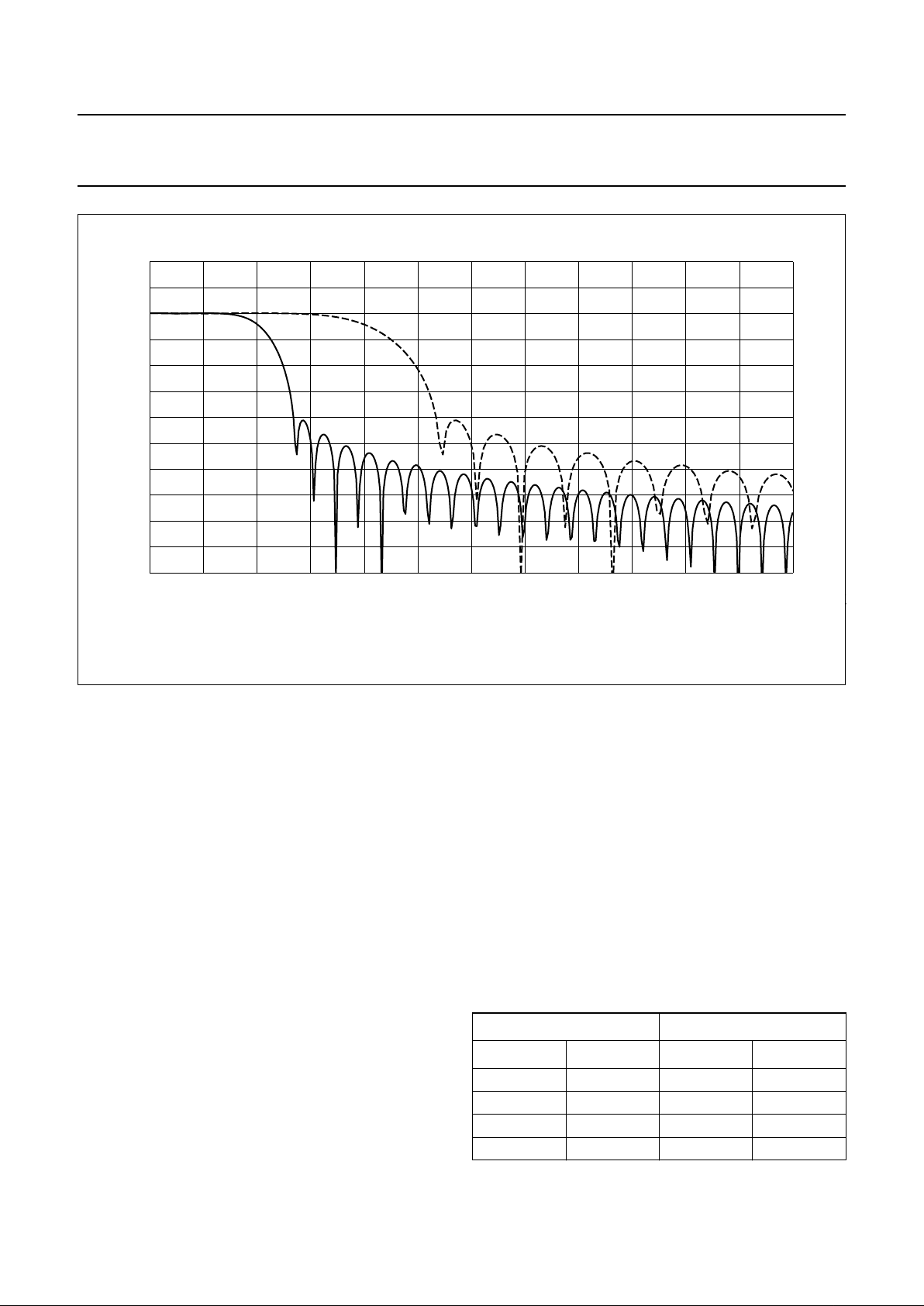
The baseband receive section can be switched between
two modes of operation:
• ZIF (zero IF) mode for radio sections, which convert the
receive signal down to baseband. In this mode the ADC
is sampled at 6.5 MHz, the decimation filter samples
down by a factor of 24 with a pass band as specified in
Fig.3. The serial interface output BDIO delivers
2 × 12-bit values for I and Q components at
270.833 kHz.
• NZIF (near zero IF) mode for radio sections, which
converts the receive signal down to a centre frequency
of 100 kHz. In this mode the ADC is sampled at 13 MHz,
the decimation filter samples down by a factor of 24 with
a pass band as specified in Fig.3. The serial interface
output BDIO delivers 2 × 12-bit values for I and Q
components at 541.667 kHz.
9.2.1 R
ECEIVE ADC
The receive ADCs are Σ∆ analog-to-digital converters that
convert differential input signals into1-bit data streams with
a sampling frequency of 6.5 or 13 MHz.
9.2.2 D
IGITAL DECIMATION FILTER
Digital filtering is required for:
• Suppression of out-of-band noise produced by the
Σ∆ ADC
• Decimation of the sampling rate (6.5 or 13 MHz) by 24
• System level filtering.
The digital filtering is performed by a digital FIR filter with a
group delay for this running average filter of approximately
23 or 11.5 µs respectively. The filter uses twos
complement arithmetic.
1999 May 03 11
Philips Semiconductors Objective specification
Baseband and audio interface for GSM PCF50732
Fig.3 Transfer functions for the baseband receive filter.
3
handbook, full pagewidth
600500
f (kHz)
20
0
gain
(dB)
100 200 300 400
−20
−40
−60
−80
−100
0
MBL025
ZIF
NZIF
9.3 Baseband Serial Interface (BSI)
9.3.1 O
VERVIEW
The digital part of the baseband consists of a receive
section and a transmit section. The receive section is a
FIR filter that reduces the 6.5 MHz (13 MHz for
NZIF mode) bitstream from the sigma-delta converters
into 2 × 12-bit values at 270.833 kHz (541.667 kHz for
NZIF mode).
The transmit section converts the 270.833 kHz data
stream from the DSP into a GMSK signal sampled at
4.333 MHz. The 10-bit I and Q signals are then fed into
two 10-bit DACs. The power ramping signal is also
generated by the transmit section with the 10-bit
AUXDAC3 block.
9.3.2 T
RANSMIT PATH BLOCK DESCRIPTION
9.3.2.1 Transmit serial interface
The power-up of the BSI transmit path is controlled via the
TXON pin. When TXON is pulled HIGH, the transmit path
recovers from power-down. The MCLK/48 = 270.833 kHz
output signal BIOCLK is activated. When the BIEN0 period
has elapsed the output signal BIEN goes LOW and the bits
to be transmitted are clocked out of the DSP.
BIEN0 must be at least 10 quarterbits long to allow settling
of the analog filters. Bits are clocked out of the DSP by the
falling edge and clocked into the PCF50732 by the rising
edge of BIOCLK. After the BIEN1 period has elapsed,
BIEN is set HIGH again and transmission from the DSP
ends. Logic 1s are modulated whenever BIEN is HIGH
and the baseband transmit (BBTX) block is active. Values
for BIEN0 and BIEN1 can be set in the Burst control
register.
Figure 5 shows the timing for the BSI data transmission.
In power-down the de-asserted value of BIOCLK is high-Z
and BIEN is HIGH. Typical connection to the system DSP
is defined in Table 1.
Table 1 Connection of BSI transmit signals to
PCF5087X
PCF50732 PCF5087X
PIN I/O PIN I/O
TXON I RFSIG[y] O
BDIO I/O SIOXD I/O
BIEN O SOXEN_N I
BIOCLK O SIOXCLK I

1999 May 03 12
Philips Semiconductors Objective specification
Baseband and audio interface for GSM PCF50732
9.3.2.2 Power ramping controller
The PCF50732 fully supports all multislot modes which do
not require full duplex operation or more than two
consecutive transmit bursts. In this specification double
burst mode is used for all supported multislot modes while
single burst mode supports the normal GSM modes.
The power ramping controller drives the power amplifier
output envelope.
In each transmit (TX) burst one ramp-up and one
ramp-down will be carried out. In multislot mode one
intermediate ramp will be carried out in addition to ramp-up
and ramp-down. Each ramp consists of 16 discrete step
values that are sent to the DAC3. Each step’s duration is
2 quarterbits which translates into 8-bit long ramps.
The DAC3 output is in 3-state whenever it is powered
down. The ramping step values are stored in a 64 × 10-bit
RAM as shown in Table 2.
In order to initialize AUXDAC3 it is necessary to write into
the RAM all 32 (or 48 in multislot mode) DAC3 output
values. Filling the RAM is normally done by writing a
logic 0 to the address sub-register of the Burst control
register, after which 32 or 48 values, depending on
multislot mode, can be written into the data sub-register of
the Burst control register. Writing to the DAC3 RAM is only
possible when the DAC3 is powered off.
Total number of CSI-accesses is therefore 33 for a normal
burst and 49 for a double burst.
An autoincrement feature will store these data into the
correct RAM positions.
The value after power-up of DAC3 will always be equal to
the value of RAM location 47.
AUXDAC3 timing is controlled by the Burst control
register. This contains the following sub-registers:
• The RU register containing the delay in number of
quarterbit cycles from the assertion of TXON to the start
of the power-up ramping; default value is 0
• The RM register containing the delay in number of
quarterbit cycles from the assertion of TXON to the start
of the intermediate power ramp; default value is 0. RM
is only used in case of multislot mode
• The RD register containing the delay in number of
quarterbit cycles from the assertion of TXON to the start
of the power-down ramping; default value is 0
• DAC3 burst RAM address register
• DAC3 burst RAM data register
• Single/double burst mode register: normal mode or
multislot mode selection flag.
After TXON goes HIGH and a time equal to RU quarterbit
periods has elapsed, power ramp-up is done.
After a time period equal to RD quarterbits has elapsed
power ramp-down is initiated.
The AUXDAC3 output is also shown in Fig.4.
Values for RU (ramp-up) and RD (ramp-down) can be set
in the Burst control register of the control serial interface.
RD must be greater than RU + 32. RU and RD range
from 0 to 4000 QB (quarterbit). The register offers the
possibility to enter codes up to 4095.
The GMSK modulator is active for a period of 2 clock
cycles after the ramp-down or for the length of the TXON
burst, whichever is longer.
Multislot (high speed switched data mode) can be selected
by setting the appropriate bit in the Burst control register.
In multislot mode an intermediate ramping step is done.
This intermediate step is started after a time period equal
to RM quarterbits has elapsed. A value for RM
(intermediate ramp) is also set using the Burst control
register. The following conditions must be true:
RU + 32 < RM and RM + 32 < RD.
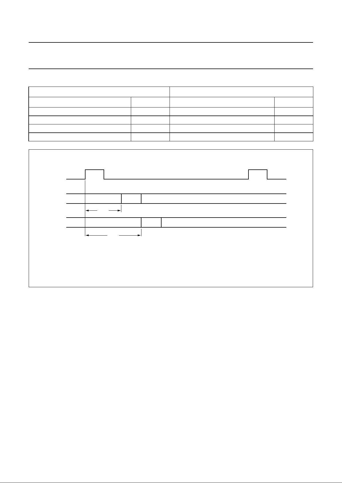
Table 2 AUXDAC3 RAM contents
Table 3 Power ramping timing characteristics
Note
1. QB: Quarterbit, usually referred to the time needed for
one quarter of a GSM baseband bit, i.e. a frequency of
1
⁄12× 13 MHz.
RAM ADDRESS DATA
0 to 15 ramp-up data
16 to 31 intermediate ramp data
32 to 47 ramp-down data
48 to 64 not used
SYMBOL VALUE COMMENTS
(1)
t
0
12t
1
one quarterbit (QB)
t
ru
RU register 0 to 4000 QB
t
im
RM register RU + 32 to 4000 QB
t
rd
RD register RM + 32 to 4000 QB
t
rup
, t
rim
, t
rdo
32t
0
8 bits; 32 QB
1999 May 03 13
Philips Semiconductors Objective specification
Baseband and audio interface for GSM PCF50732
Fig.4 Power ramping timing characteristics (multislot mode).
(1) APE_DAC3: Analog Power Enable signal for the AUXDAC3.
andbook, full pagewidth
MGR995
t
rup
t
rim
t
rdo
RU RM RD
t
ru
AUXDAC3
TXON
APE_DAC3
(1)
ADDRESS
AUXDAC3
RAM
0
15 15 31
31 47154747
31
47
t
im
t
rd
9.3.3 RECEIVER PATH BLOCK DESCRIPTION
9.3.3.1 Receive serial interface
The baseband serial interface sends the digital signal of
the receive path to a digital signal processor. It also takes
the digital bitstream from the digital signal processor and
transmits it via the baseband CODEC.
The baseband reception and transmission are active in
bursts. A normal burst has a length of 548 µs. The frame
rate of bursts is 4.615 ms. Using a normal traffic channel,
one burst for each frame is transmitted and two bursts are
received. To save as much power as possible, the transmit
path and the receive path of the PCF50732 are in
power-up mode only during the transmission or reception
bursts respectively.
The power-up of the receive section is controlled via the
RXON pin or RXON bit. When RXON is driven HIGH, the
receive section recovers from power-down and the output
clock BIOCLK is activated. After a settling delay of 52 µs
(ZIF mode, analog circuitry + decimation filter settling
time), BOEN goes LOW to transfer the first 12-bit
I and Q words. The settling time is only 26 µs in NZIF
mode.
Bits are clocked out of the PCF50732 by the falling edge,
and clocked into the DSP by the rising edge of BIOCLK.
In normal bursts 148 I/Q pairs are read from the
PCF50732.
When RXON goes LOW, the last pair of I and Q values will
be sampled and transferred to the baseband processor
(both I and Q components). BIOCLK stops after additional
16 BIOCLK cycles. The receive path is powered down
again. In power-down the BIOCLK output is put in 3-state
and the BOEN output is HIGH.
The output format is 2 × 12-bit I/Q (twos complement).
Transmission occurs MSB first, I followed by Q. The serial
clock signal BIOCLK will run at 6.5 MHz, or 13 MHz in the
NZIF mode. Figure 6 shows the timing of the BSI data
reception.
An automatic offset compensation mechanism is provided
in order to achieve the required performance. This
mechanism will short the receive (RX) inputs internally and
measure the resulting offset value. This offset value will be
subtracted from all subsequent I/Q output words.
The offset inherent to the device can thereby be reduced
to a few millivolts. Default value for both I- and Q-offset is
zero.

1999 May 03 14
Philips Semiconductors Objective specification
Baseband and audio interface for GSM PCF50732
Offset compensation measurement can be done on three
channels separately: baseband receive I channel,
baseband receive Q channel and AUXADC channel. All
AUXADC channels use the same offset compensation
value. Starting an offset measurement is done by writing a
logic 1 into the offset trigger register for each channel that
needs calibration. If the value ‘7’ (decimal) is written into
the offset trigger register offsets will be measured for I, Q
and AUXADC channels.
Offsets can also be read or written directly. Each offset
measurement is implemented internally as an AUXADC
measurement and takes approximately 100 µs.
Offsets from −256 up to 255 can be compensated.
Table 4 Connection of BSI receive signals to the
PCF5087X
PCF50732 PCF5087X
PIN I/O PIN I/O
RXON I RFSIG[z] O
BDIO I/O SIOXD I/O
BOEN O SIXEN_N I
BIOCLK O SIOXCLK I
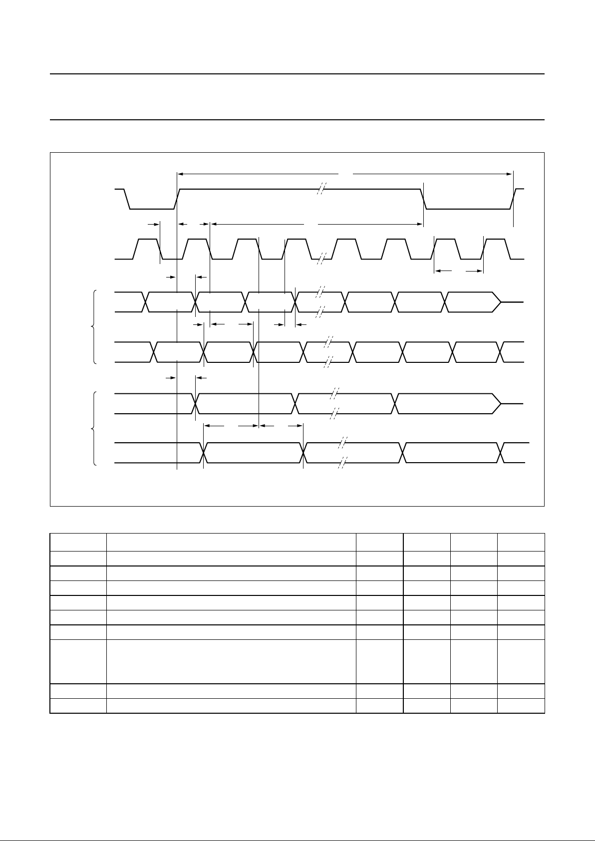
9.3.4 BASEBAND SERIAL INTERFACE (BSI) TIMING CHARACTERISTICS
handbook, full pagewidth
MGR990
t
39
t
9
t
10
d.c.
(2)
logic 1s
logic 1s
data
data
data
data
d.c. d.c. B(0) B(n)B(1)
t
6
t
7
t
42
t
44
t
40
ramp-up
32 QB
intermediate ramp
32 QB
trail
2 BIOCLK
clocks
ramp-down
32 QB
t
43
high-Zhigh-Z
high-Zhigh-Z
BIOCLK
AUXDAC3
TXI/Q
(1)
BDIO
BIEN
TXON
t
5
Fig.5 Timing of the baseband serial interface transmit path; for the timing values see Table 5
(1) TXI/Q = transmit I or Q.
(2) d.c. = don’t care; will be overwritten with logic 1.
1999 May 03 15
Philips Semiconductors Objective specification
Baseband and audio interface for GSM PCF50732
Table 5 BSI timing characteristics
SYMBOL PARAMETER MIN. TYP. MAX. UNIT
Master clock
t
1
MCLK cycle time − 76.9 − ns
t
2
MCLK LOW time 30
1
⁄2t
1
− ns
t
3
MCLK HIGH time 30
1
⁄2t
1
− ns
t
4
RESET LOW time 3t
1
−−ns
Baseband Serial Interface (BSI) transmit path (see Fig.5)
t
5
BIEN0 value 10 − 511 QB
t
6
BIEN1 value t
5
− 4000 QB
t
7
BIOCLK cycle time − 48t
1
− ns
t
9
data set-up time 20 −−ns
t
10
data hold time 20 −−ns
t
39
BIOCLK active after TXON rising edge −−t
1
ns
t
40
analog TX and GMSK power-up time −−17.4 QB
t
42
ramp-up value 0 − 3940 QB
t
43
intermediate ramp value 32 + t
42
− 3980 QB
t
44
ramp-down value
normal mode 32 + t
42
− 4020 QB
double burst mode 32 + t
43
− 4020 QB
Fig.6 Timing of the baseband serial interface receive path; for the timing values see Table 5.
handbook, full pagewidth
MGR991
t
14
t
13
I11 I0 Q11 Q0
t
15
t
11
548 µs
t
12
16t
1
high-Zhigh-Z
BIOCLK
BDIO
BOEN
RXON

1999 May 03 16
Philips Semiconductors Objective specification
Baseband and audio interface for GSM PCF50732
Baseband Serial Interface (BSI) receive path (see Fig.6)
t
11
analog power-up and filter settling time
ZIF mode − 52 −µs
NZIF mode − 26 −µs
t
12
BIOCLK cycle time
ZIF mode − 2t
1
− ns
NZIF mode − t
1
− ns
t
13
BOEN LOW after falling clock edge −−15 ns
t
14
BIOCLK falling edge to data valid −−15 ns
t
15
BOEN HIGH after falling clock edge −−15 ns
SYMBOL PARAMETER MIN. TYP. MAX. UNIT
10 VOICE BAND CODEC
The voice band CODEC is a complete analog front-end
circuit. It consists of three parts:
• The receive path, which converts a digital linear PCM
signal to an analog signal for an earpiece, an external
loudspeaker or a buzzer
• The transmit path, which receives an analog signal
from a microphone or an auxiliary input and converts it
into a digital linear PCM signal
• The digital Audio Serial Interface (ASI), which
connects the digital linear PCM signals of the receive
and transmit paths to a digital signal processor.
Various functions and characteristics of the voice band
CODEC can be selected by programming the
corresponding control registers in the Control register
block (see also Tables 11, 22, 23, 24 and 25).
10.1 Voice band receive path
The voice band receive path consists of the following
parts:
• The receive part of the voice band signal processor
• NOISE SHAPER: 3rd order digital Σ∆ modulator,
generates a bit stream at 1 MHz to drive the EARDAC
• EARDAC: digital-to-analog converter including
low-pass filter for high frequency noise content of noise
shaper
• EARAMP: amplifier for an earpiece
• AUXAMP: amplifier for an auxiliary loudspeaker
• BUZAMP: amplifier for a buzzer output.
Linearity of receiver equipment (to earpiece) at
EARPGA = 0 dB and a volume control (VOLPGA and
EARAMP or AUXAMP) of−12 dB, signal-to-total harmonic
distortion ratio according to
“GSM recommendation
II.11.10 V.4.16.1”
.
10.1.1 RXVOL
RXVOL controls the volume of the voice band receive
path. In conjunction with EARAMP, AUXAMP and
BUZAMP it allows a gain variation from +6 to −30 dB in
64 steps; see Table 25. RXVOL also provides a mute
selection of the three outputs EARP/EARN, AUXSP and
BUZ respectively. At
RESET the volume is automatically
set to −12 dB.
10.1.2 RXPGA
RXPGA controls the gain of the voice band receive path
within a range of −24 to +12 dB in 64 steps for calibration
purposes.
10.1.3 RXFILTER
RXFILTER is a digital band-pass filter with a pass band
from 300 to 3400 Hz. It is realized by a programmable
structure (voice band signal processor).
10.1.4 EARDAC
EARDAC is a DAC operating at a sampling frequency of
1 MHz. It converts the bitstream input to a sampled
differential analog signal and low-pass filters the output
signal at the same time.

1999 May 03 17
Philips Semiconductors Objective specification
Baseband and audio interface for GSM PCF50732
10.1.5 EARAMP
EARAMP is an amplifier, capable of driving a standard
earpiece with a minimum impedance of 8 Ω in
single-ended mode or 16 Ω in differential mode.
10.1.6 AUXAMP
AUXAMP is an amplifier for connection to an external
loudspeaker amplifier of minimum 8 Ω (hands-free car kit).
An‘auxiliary speaker external amplifier control’ output
pin (AMPCTRL) can be used to switch on/off an external
amplifier (hands-free car kit). The status of AMPCTRL is
programmable via the Control Serial Interface; its default
value is on.
10.1.7 BUZAMP
BUZAMP is an amplifier for connection to an external
buzzer of minimum 8 Ω. It has the same output
characteristics as the AUXAMP and can hence be used as
a second auxiliary output amplifier. It is switched on/off by
a dedicated control bit in the Control register block.
10.2 Voice band transmit path
The voice band transmit path consists of the following
parts:
• MICMUX: microphone input multiplexer
• MICADC: Σ∆ analog-to-digital converter
• DECIMATOR: decimates the incoming bit stream from
1 MHz to 40 kHz
• TXFILTER: band-pass filter for the digital transmit signal
and down-sampling
• TXPGA/LIM: fine-programmable gain for calibration,
limiter
• SidePGA: voice band sidetone programmable gain
amplifier.
Linearity of transmitter equipment, signal-to-total harmonic
distortion ratio according to
“GSM recommendation
II.11.10 V.4.16.1”
.
10.2.1 MICMUX
MICMUX is used to select between a differential signal at
pins MICP/MICN and a differential signal at pins
AUXMICP/AUXMICN.
Values are specified for a standard electret microphone
with a sensitivity of −64 ±3 dB for high gain or for an
external microphone with an amplifier sensitivity of
−26 ±3 dB (0 dB ≡ 1 V/0.1 Pa = 1 V/µbar; at 1 kHz).
10.2.2 MICADC
MICADC is a Σ∆ A/D converter which generates a 1 MHz
bitstream.
10.2.3 DECIMATOR
AND TXFILTER
The DECIMATOR is a digital filter, which performs a signal
processing to a lower sampling rate at the output
compared to the input.
The bitstream with a sampling frequency of 1 MHz is
low-pass filtered and down-sampled to 40 kHz by a FIR
filter.
A digital high-pass filter and a digital low-pass filter (both
IIR filters) process the 14-bit input samples to achieve a
band-pass with a pass band from 300 to 3400 Hz. These
filters run on the on-chip voice band signal processor (see
Fig.7). It’s program is down-loaded into the instruction
memory (IRAM) via the CSI (see Table 26).
The output of the TXFILTER is down-sampled to a
sampling frequency of 8 kHz with a word length of 16 bits.
10.2.4 TXPGA
TXPGA adapts the analog signals coming from MICMUX
within a range of−30 to +6 dB. It is designed for calibration
purposes.
10.2.5 SIDEPGA
SidePGA loops part of the voice band transmit signal back
into the receive path. There are 64 gain steps from mute to
+6 dB.
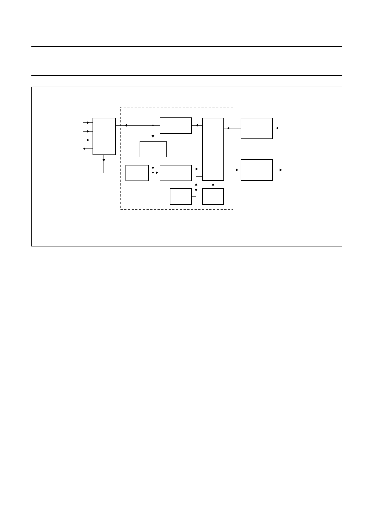
10.3 Voice band digital circuitry
The voice band digital circuitry is responsible for
converting a 16-bit PCM signal at 8 kHz sample rate to and
from a 1-bit 1 MHz signal. It also contains a band-pass
filter for 300 to 3400 Hz and a sidetone engine. Various
volume settings are calculated inside this block. Figure 7
shows the block diagram of the voice band signal
processor.
1999 May 03 18
Philips Semiconductors Objective specification
Baseband and audio interface for GSM PCF50732
Fig.7 Block diagram of the voice band signal processor.
handbook, full pagewidth
MGR992
DECIMATOR
16-bit, 8 kHz
1-bit, 1 MHz
ASI
ADI
ACLK
AFS
ADO
RX_BS
(receive bitstream)
TX_BS
(transmit bitstream)
RX/TX
FILTER
VOICE BAND SIGNAL PROCESSOR
TXPGA/LIM
RXPGA/LIM
RXVOL
SidePGA
RRAM IRAM
NOISE
SHAPER
10.3.1 VOLUME CONTROL BLOCK
The volume control block contains the RXPGA, SidePGA,
TXPGA and both limiter blocks. The possible settings can
be found in the description of the CSI block. All digital
volume control blocks, i.e. RXPGA, SidePGA, and
TXPGA, will allow settings from +6 to −30 dB and mute in
64 steps. However, not all combinations of settings for
these blocks will be meaningful. The limiter will always clip
signals with overflow to the maximum or minimum
allowable value.
10.3.2 A
UDIO SERIAL INTERFACE (ASI) BLOCK
The ASI is the voice band serial interface which provides
the connection for the exchange of PCM data in both
receive and transmit directions, between the baseband
digital signal processor and the PCF50732. The data is
coded in 16-bit linear PCM twos complement words.
A frame start is defined by the first falling edge of ACLK
after a rising AFS. This first falling edge is used to clock in
the first data bit on both the baseband and the DSP device.
Data on pin ADI is clocked in (MSB first) on the falling edge
of the ACLK clock. Data is clocked out (MSB first) on pin
ADO on the rising edge of the ACLK clock.
Pin ADO is put in 3-state after the LSB of the transmit
word, independent of the length of the AFS pulse. If the
channel position 0 (see Section 10.3.2.1) is selected, then
the MSB must be output directly after AFS becomes a
logic 1, even if no rising edge on ACLK has been given yet.
The following modes of operation are programmable:
channel position and ACLK clock mode.
10.3.2.1 Channel position mode
Depending on a programmable register value n
(n = 0 to 15) one of 16 channels can be selected (see
Table 22). The ASI can add a delay of 16 × n-bit clocks
between the assertion of AFS and the start of the MSB of
the PCM values. This delay is independently
programmable for transmit and receive mode.
10.3.2.2 ACLK clock mode
Single or double clock mode can be selected. Double clock
mode implies two clock pulses per data bit and is used for
communication with IOM2 compatible devices. In double
clock mode data must be output on the first rising edge and
be read on the last falling edge.
1999 May 03 19
Philips Semiconductors Objective specification
Baseband and audio interface for GSM PCF50732
Table 6 Pin connection of the audio serial interface to the PCF5087X
PCF50732 PCF5087X
PIN I/O PIN I/O
ADI I DD O
ADO O DU I
ACLK I DCL O
AFS I FSC O
Fig.8 Frame structure of the Audio Serial Interface (ASI).
t
rpdc
: receive path data channel delay.
t
tpdc
: transmit path data channel delay.
handbook, full pagewidth
MGR993
word
word
AFS
ADI
ADO
t
tpdc
t
rpdc
1999 May 03 20
Philips Semiconductors Objective specification
Baseband and audio interface for GSM PCF50732
10.3.2.3 Audio Serial Interface (ASI) timing characteristics
Table 7 ASI timing characteristics
SYMBOL PARAMETER MIN. TYP. MAX. UNIT
t
16
frame sync (AFS) set-up time to falling edge of ACLK 70 −−ns
t
17
frame sync (AFS) hold time from falling edge of ACLK 40 −−ns
t
18
ACLK rising edge to data (ADO) valid −30 − +30 ns
t
19
data (ADI) set-up time to falling edge of ACLK 50 −−ns
t
20
data (ADI) hold time from falling edge of ACLK 80 −−ns
t
21
first data valid (ADO) after AFS rising edge 0 − 60 ns
t
40
ACLK period
single clock mode 0.5 − 7.8 µs
double clock mode 0.5 − 3.9 µs
t
41
AFS period − 125 −µs
t
42
ACLK LOW before AFS rising edge 40 −−ns
Fig.9 Timing of the Audio Serial Interface (ASI).
handbook, full pagewidth
MGR994
single
clock
mode
ADO
ACLK
AFS
ADI
t
41
last slot
last bit
last slot
last bit
first slot
first bit
MSB
LSB
first slot
second bit
last slot
last bit
last slot
last bit
first slot
first bit
MSB LSB
first slot
second bit
double
clock
mode
ADO
ADI
last slot
last bit
last slot
last bit
first slot
first bit
MSB LSB
high-Z
high-Z
slot 1
bit 2
last slot
last bit
last slot
last bit
first slot
first bit
MSB
LSB
slot 1
bit 2
t
16
t
42
t
17
t
40
t
21
t
20
t
18
t
19
t
19
t
20
t
21
 Loading...