

查询PCF50603供应商
INTEGRATED CIRCUITS
DATA SH EET
PCF50603
Controller for power supply
and battery management
Preliminary specification 2003 Oct 31

Philips Semiconductors Preliminary specification
Controller for power supply
and battery management
CONTENTS
1 FEATURES
1.1 System control
1.2 Supply voltage generation
1.3 Battery management
1.4 Subscriber identity module card interface
2 APPLICATIONS
3 GENERAL DESCRIPTION
4 QUICK REFERENCE DATA
5 ORDERING INFORMATION
6 BLOCK DIAGRAM
7 PINNING
8 FUNCTIONAL DESCRIPTION
8.1 On/off control
8.1.1 Operating states
8.1.2 Reset generation
8.1.3 Watchdog timer
8.1.4 Automatic restart after battery removal
8.1.5 Debounce filters
8.2 Serial interface (I2C-bus)
8.3 Interrupt controller (INT)
8.4 Power supply modules
8.5 Main battery charger (MBC)
8.5.1 Supported charger plugs
8.5.2 External components
PCF50603
8.6 Backup battery charger (BBC)
8.7 SIM card interface (SIMI)
8.8 Battery voltage monitor (BVM)
8.9 Temperature high sensor (TS)
8.10 Real time clock (RTC)
8.11 Pulse-width modulator (PWM1 and PWM2)
8.12 LED modulator (LED1 and LED2)
8.13 General purpose outputs (GPO)
9 LIMITING VALUES
10 CHARACTERISTICS
11 APPLICATION INFORMATION
12 PACKAGE OUTLINE
13 SOLDERING
13.1 Introduction to soldering surface mount
packages
13.2 Reflow soldering
13.3 Wave soldering
13.4 Manual soldering
13.5 Suitability of surface mount IC packages for
wave and reflow soldering methods
14 DATA SHEET STATUS
15 DEFINITIONS
16 DISCLAIMERS
17 PURCHASE OF PHILIPS I2C COMPONENTS
2003 Oct 31 2

Philips Semiconductors Preliminary specification
Controller for power supply
and battery management
1 FEATURES
1.1 System control
• Serial 400 kHz I2C-bus interface to transfer the control
data between the PCF50603 and the host controller
• On/Off Control (OOC) module to control the power
ramp-up and ramp-down sequences for the handset.
Furthermore it determines the supported system
operating states: NOPOWER, SAVE, STANDBY and
ACTIVE to realize minimum power consumption in all
states.
• Internal Current Controlled Oscillator (CCO) generates
the internal high clock frequency. The generated
frequency is typically 3.6 MHz.
• Anaccurate32.768 kHzoscillator.Thisoscillatorcanbe
used to supply the 32 kHz clock domains in the system,
to improve the accuracy of the internal clock and to
reduce the power consumption of the PCF50603.
• Interrupt controller (INT) that generates the interrupt
request for the host controller. All interrupt sources can
be masked.
• The Real Time Clock (RTC) module uses the 32 kHz
clock to provide time reference and alarm functions with
wake up control for the handset
• Oneaccessory recognition pin with debounce filters and
capability to start up the system (REC1_N)
• One accessory detection comparator input pin with
programmable threshold levels that issues an interrupt
when an accessory is connected (REC2_N)
• TwoPulse-WidthModulators(PWM1andPWM2)which
generate an output voltage with programmable duty
cycle and frequency
• Two LED modulators (LED1 and LED2) capable of
generating eight different blinking patterns with eight
different repetition periods
• Three General Purpose Outputs (GPO) programmable
via the serial interface. The GPOs are open-drain
NMOST outputs, capable of handling the full battery
voltage range and high sink currents. The GPOs can be
programmed to be continuously active LOW or 3-state,
in addition the GPO outputs can be controlled by the
LED or PWM modulators.
• Watchdog timer that can be activated by software.
PCF50603
1.2 Supply voltage generation
• The power supplies have three programmable activity
modes (OFF, ECO and ON). In the ACTIVE state, the
operation modes can be selected by the two external
pins PWREN1 and PWREN2.
• One Charge Pump (CP) with programmable output
voltage for the supply of white or blue LEDs
• Two 100 mA LDO voltage regulators (RF1REG and
RF2REG) with fixed output voltage (mask
programmable) for RF supplies. RF1REG and RF2REG
are optimized for low noise, high power supply rejection
and excellent load regulation.
• Two 150 mA LDO voltage regulators (D1REG and
D2REG) optimized for small external capacitors.
D1REG provides a programmable output voltage,
D2REG provides a fixed output voltage (mask
programmable).
• One 150 mA LDO voltage regulator (IOREG) dedicated
for the supply of the I/O pads. IOREG has a fixed output
voltage (mask programmable) and is optimized for a
small external capacitor.
• One 100 mA LDO voltage regulator (LPREG) with fixed
output voltage (mask programmable). In low power
operation (ECO) mode LPREG can be used to
permanently supply parts in the system in all activity
states.
• One 100 mA LDO voltage regulator (D3REG) with
programmableoutputvoltage.D3REGisoptimizedfora
small external capacitor.
• One 250 mA LDO voltage regulator (HCREG) with
programmableoutputvoltage. The high current HCREG
is optimized for applications like hands-free audio.
• D1REG, D2REG, D3REG, IOREG and LPREG support
ECO mode. In this mode the output current is limited to
1 mA and the internal power consumption is reduced
significantly.
• The Temperature high Sensor (TS) provides thermal
protection for the whole chip
• Enhanced ESD protection on all pins that connect to the
main battery pack
• Microphone bias voltage generator with low noise and
high power supply rejection (MBGEN).
2003 Oct 31 3

Philips Semiconductors Preliminary specification
Controller for power supply
and battery management
1.3 Battery management
• Operates from a three cell NiCd/NiMH or a one cell
Li-ion battery pack
• Battery Voltage Monitor (BVM) to detect a too low main
battery voltage with programmable threshold levels.
A low battery condition is reported via the interrupt
mechanism.
• Charger control. There is an option between two
different charger control functions, depending on the
configuration:
– Configuration Constant Current Constant Voltage
(CCCV). Linear charger control supporting Li-ion as
well as NiCd/NiMH battery types for a wide range of
battery capacities.
– Configuration BATMAX comparator that compares
the battery voltage against a programmable
threshold voltage. This function can be activated by
software and is used to detect the end-of-charge.
• Supports the use of a backup battery that powers at
empty main battery situations. The backup battery is
used to supply the RTC, the internal state and the
LPVDDsupplyinit’sECOmode.Goldcaps,LiandLi-ion
cells are supported.
• Includes a Backup Battery Charger (BBC).
A rechargeable backup battery or backup capacitor can
be charged from the main battery. For charging, a
programmable constant voltage mode is supported.
PCF50603
1.4 Subscriber identity module card interface
• Two different modes that can be selected with the
Subscriber Identity Module card Interface (SIMI):
– Transparent interface including an arbiter and signal
level translators
– Subscriber Identity Module (SIM) card interface with
integrated sequencer, arbiter and signal level
translators. The sequencer supports and controls
card activation and de-activation, warm reset and
controlled clock stop for power-down modes.
• Dedicated SIM supply (SIMREG). Supports
3.0 V and 1.8 V cards, including a power saving ECO
mode for the power-down mode of the SIM card.
• Enhanced ESD protection on all pins that connect to the
SIM card contact pins.
2 APPLICATIONS
• Mobile phones.
3 GENERAL DESCRIPTION
The PCF50603 is a highly integrated solution for power
supply generation, battery management including
charging and a SIM card interface including supply
generation.Thedeviceiscontrolledbyahostcontrollervia
a 400 kHz I2C-bus serial interface.
4 QUICK REFERENCE DATA
VSS= REFGND = GND = 0 V; T
= −40 °C to +85 °C; unless otherwise specified.
amb
SYMBOL PARAMETER CONDITIONS MIN. TYP. MAX. UNIT
V
V
V
BAT
SAVE
CHG
main battery input voltage 0 − 5.7 V
backup battery input voltage 0 − 5.7 V
charger input voltage DC 0 − 15.0 V
rectified sine wave;
0 − 20.0 V
100 Hz to 120 Hz; note 1
V
CHGMIN
minimum charger voltage
− 2.7 − V
enabling MBC module
f
CLKCCO
high clock frequency 32 kHz clock available 3.42 3.6 3.78 MHz
Note
1. Not allowed in CCCV configuration.
2003 Oct 31 4

Philips Semiconductors Preliminary specification
Controller for power supply
and battery management
5 ORDERING INFORMATION
PACKAGE
TYPE NUMBER
NAME DESCRIPTION VERSION
PCF50603HN HVQFN48 plastic thermal enhanced very thin quad flat package; no leads;
48 terminals; body 6 × 6 × 0.85 mm
PCF50603
SOT778-1
2003 Oct 31 5
Philips Semiconductors Preliminary specification
Controller for power supply
and battery management
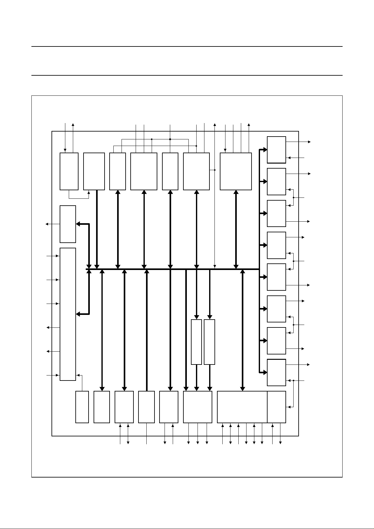
6 BLOCK DIAGRAM
OSCI
OSCO
25
26
UNIT
CLOCK
GENERATOR
BBC
IRQ_N
32kHz
OSCILLATOR
INT
CONTROLLER
CHGDRV
CHGCUR/
BATMAX
34
33
AND
BATMAX
COMPARATOR
MBC
31
BAT
V
BVM
SAVEVCHG
V
30
32
SUPPLY
MODULE
INTERNAL
VINT
29
CPVBAT
SCP
363738
CP
SCN
CPVDD
35
PCF50603
MDB679
HCREG
RF2REG
RF1REG
18 17
24
2320
22
19
RF1VDD RF2VDD HCVDDD3VDD
book, full pagewidth
27 11 4 6 5 101
ONKEY_N RSTHC_N CLK32K PWREN1 PWREN2 REC1_N
OOC
TS
PCF50603
system clocks
operation modes
temp_ok
ALARM
RTC AND
status data
control data
C-BUS
2
I
INTERFACE
3
2
reference voltage
bias currents
ON-CHIP
28
AUDIO
REFERENCE
DETECTION
12
13
PWM1 AND PWM2
GPO
48
47
46
internal supply
LED1 AND LED2
8
9
7
SIMI
434244
45
LPREG
D1REG
D2REG
IOREG
D3REG
SIMREG
41
LPD1VBAT LPVDD RF12VBAT HCVBAT
21
D1VDD
16
Fig.1 Block diagram.
14 15
40 39
SIMD3VBAT IOVDD IOD2VBAT D2VDD
This text is here in white to force landscape pages to be rotated correctly when browsing through the pdf in the Acrobat reader.This text is here in
_white to force landscape pages to be rotated correctly when browsing through the pdf in the Acrobat reader.This text is here inThis text is here in
white to force landscape pages to be rotated correctly when browsing through the pdf in the Acrobat reader. white to force landscape pages to be ...
2003 Oct 31 6
SCL
SDA
REFC
REC2_N
MICBIAS
GPO1
GPO2
GPO3
SIMIOHC
SIMCKHC
SIMIOCD
SIMCKCD
SIMRSHC_N
SIMEN
SIMVCC
SIMRSCD_N

Philips Semiconductors Preliminary specification
Controller for power supply
PCF50603
and battery management
7 PINNING
SYMBOL PIN SUPPLY DESCRIPTION
VSS and
REFGND
− n.a. ground and VSS pads of all modules are connected to the ground plane of the
package
REC1_N 1 VINT accessory recognition input with debounce filter (active LOW); input with internal
pull-up resistor to VINT
2
SCL 2 IOVDD I
SDA 3 IOVDD I
C-bus clock input
2
C-bus data input and output
CLK32K 4 IOVDD 32.768 kHz digital clock output; in ACTIVE state and IOVDD is on
PWREN2 5 IOVDD control signal input; selects in combination with PWREN1 the ON, OFF or ECO
mode of the linear regulators
PWREN1 6 IOVDD control signal input; selects in combination with PWREN2 the ON, OFF or ECO
mode of the linear regulators
SIMRSHC_N 7 IOVDD SIM reset input from host controller (active LOW)
SIMCKHC 8 IOVDD SIM clock input from host controller
SIMIOHC 9 IOVDD SIM I/O data to or from the host controller with an internal pull-up resistor to
IOVDD
IRQ_N 10 IOVDD interrupt request output to host controller (active LOW); open-drain output with an
internal pull-up resistor to IOVDD
RSTHC_N 11 IOVDD reset output to host controller (active LOW)
MICBIAS 12 n.a. microphone bias output voltage
REC2_N 13 MICBIAS accessory recognition input with debounce filter and programmable threshold
(active LOW)
IOVDD 14 n.a. IOREG output voltage
IOD2VBAT 15 n.a. IOREG and D2REG input voltage
D2VDD 16 n.a. D2REG output voltage
HCVDD 17 n.a. HCREG output voltage
HCVBAT 18 n.a. HCREG input voltage
LPVDD 19 n.a. LPREG output voltage
LPD1VBAT 20 n.a. LPREG and D1REG input voltage
D1VDD 21 n.a. D1REG output voltage
RF1VDD 22 n.a. RF1REG output voltage
RF12VBAT 23 n.a. RF1REG and RF2REG input voltage
RF2VDD 24 n.a. RF2REG output voltage
OSCO 25 VINT 32.768 kHz oscillator output
OSCI 26 VINT 32.768 kHz oscillator input
ONKEY_N 27 VINT On-key (active LOW); input with internal pull-up resistor to VINT
REFC 28 n.a. reference voltage bypass capacitor connection
VINT 29 n.a. internal supply voltage output
V
V
V
SAVE
BAT
CHG
30 n.a. backup battery supply voltage
31 n.a. main battery supply voltage
32 n.a. charger voltage
(1)
2003 Oct 31 7

Philips Semiconductors Preliminary specification
Controller for power supply
PCF50603
and battery management
SYMBOL PIN SUPPLY DESCRIPTION
CHGDRV 33 n.a. drive of external charger circuitry (configuration CCCV)
CHGCUR/
BATMAX
CPVDD 35 n.a. charge pump output voltage
CPVBAT 36 n.a. charge pump input voltage
SCP 37 n.a. switching capacitor positive side
SCN 38 n.a. switching capacitor negative side
D3VDD 39 n.a. D3REG output voltage
SIMD3VBAT 40 n.a. SIMREG and D3REG input voltage
SIMVCC 41 n.a. SIMREG output voltage
SIMIOCD 42 SIMVCC SIM I/O data to/from the SIM card; internal pull-up resistor to SIMVCC
SIMCKCD 43 SIMVCC SIM clock output to the SIM card
SIMRSCD_N 44 SIMVCC SIM reset output to the SIM card (active LOW)
SIMEN 45 IOVDD enable SIMI and SIMREG
GPO3 46 n.a. general purpose open-drain output 3
GPO2 47 n.a. general purpose open-drain output 2
GPO1 48 n.a. general purpose open-drain output 1
34 n.a. configuration CCCV: charger current feedback
configuration BATMAX: open-drain output of BATMAX comparator
(1)
Note
1. One ESD diode reverse biased to VSSexcept pin V
between pad and VSS.
who has one clamp in series with a 500 Ω resistor connected
CHG
2003 Oct 31 8

Philips Semiconductors Preliminary specification
Controller for power supply
and battery management
handbook, full pagewidth
MICBIAS
RSTHC_N
IRQ_N
SIMIOHC
SIMCKHC
SIMRSHC_N
PWREN1
PWREN2
CLK32K
SDA
SCL
REC1_N
LPVDD
HCVDD
REC2_N
IOVDD
IOD2VBAT
1314151617181920212223
12 25
11 26
10 27
9 28
8 29
7 30
6 31
5 32
4 33
3 34
2 35
1 36
4847464544434241403938
GPO3
GPO1
GPO2
HCVBAT
D2VDD
PCF50603HN
SIMEN
SIMCKCD
SIMRSCD_N
LPD1VBAT
SIMVCC
SIMIOCD
D1VDD
RF12VBAT
RF1VDD
SCN
D3VDD
SIMD3VBAT
RF2VDD
24
37
SCP
OSCO
OSCI
ONKEY_N
REFC
VINT
V
SAVE
V
BAT
V
CHG
CHGDRV
CHGCUR/BATMAX
CPVDD
CPVBAT
MDB680
PCF50603
Bottom view.
All GND and VSS pads are connected to the ground plane.
Fig.2 Pin configuration.
2003 Oct 31 9
 Loading...