

Philips PCF5001T, PCF5001U, PCF5001H Datasheet

DATA SH EET
Product specification
Supersedes data of 1995 Apr 27
File under Integrated Circuits, IC17
1997 Mar 04
INTEGRATED CIRCUITS
PCF5001
POCSAG Paging Decoder

1997 Mar 04 2
Philips Semiconductors Product specification
POCSAG Paging Decoder PCF5001
CONTENTS
1 FEATURES
2 APPLICATIONS
3 GENERAL DESCRIPTION
4 ORDERING INFORMATION
5 BLOCK DIAGRAMS
6 PINNING
7 FUNCTIONAL DESCRIPTION
7.1 The PCF5001 supports two basic modes of
operation
7.2 The POCSAG paging code
7.3 Modes and states of the decoder
7.4 Decoding of the POCSAG data stream
7.5 Generation of output signals
7.6 Alerter
7.7 Silent call storage and Repeat mode
7.8 Duplicate Call Suppression
7.9 LED indicator
7.10 Vibrator output
7.11 Start-up alert
7.12 Serial communication interface
7.13 Message data transfer
7.14 Call Data output on LED
7.15 Serial communication call data format
7.16 Data conversion
7.17 Memory Organization
7.18 Description of the Special Programmed
Function (SPF) bits
7.19 EEPROM Write operation
7.20 EEPROM Read operation
7.21 Read-back operation via Microcontroller
Interface
7.22 Voltage converter
7.23 Test modes of the decoder
7.23.1 Board test mode
7.23.2 Pager Test Mode (Type Approval Mode)
8 LIMITING VALUES
9 DC CHARACTERISTICS
10 DC CHARACTERISTICS (WITH VOLTAGE
CONVERTER)
11 AC CHARACTERISTICS
12 TIMING CHARACTERISTICS
13 PROGRAMMING CHARACTERISTICS
14 APPLICATION INFORMATION
15 PACKAGE OUTLINES
16 SOLDERING
16.1 Introduction
16.2 Reflow soldering
16.3 Wave soldering
16.3.1 LQFP
16.3.2 SO
16.3.3 Method (LQFP and SO)
16.4 Repairing soldered joints
17 DEFINITIONS
18 LIFE SUPPORT APPLICATIONS

1997 Mar 04 3
Philips Semiconductors Product specification
POCSAG Paging Decoder PCF5001
1 FEATURES
• Wide operating supply voltage range (1.5 to 6.0 V)
• Extended temperature range: −40 to +85 °C (between
−40 to −10 °C, minimum supply voltage restricted
to 1.8 V)
• Very low supply current (60 µA typ. with
76.8 kHz crystal)
•
“CCIR radio paging Code No 1”
(POCSAG) compatible
• Programmable call termination conditions
• 512 and 1200 bits/s data rates (2400 bits/s with some
restrictions), see Section 7.4
• Improved ACCESS
synchronization algorithm
• Supports 4 user addresses (RICs) in two independent
frames
• Eight different alert cadences
• Directly drives magnetic or piezo ceramic beeper
• High level alert requires only a single external transistor
• Optional vibrator type alerting
• Silent call storage, up to eight different calls
• Repeat alarm facility
• Programmable duplicate call suppression
• Interfaces directly to UAA2050T, UAA2080 and
UAA2082 digital paging receivers
• Programmable receiver power control for battery
economy
• On-chip non-volatile EEPROM storage
• On-chip voltage converter with improved drive capability
• Serial microcontroller interface for display pager
applications
• Optional visual indication of received call data using a
modified RS232 format
• Level shifted microcontroller interface signals
• Alert on low battery
• Optional out-of-range indication.
2 APPLICATIONS
• Alert-only pagers, display pagers
• Telepoint
• Telemetry/data receivers.
3 GENERAL DESCRIPTION
The PCF5001 is a fully integrated low-power decoder and
pager controller. It decodes the CCIR radio paging Code
No.1 (POCSAG-Code) at 512 and 1200 bits/s data rates.
The PCF5001 is fabricated in SACMOS technology to
ensure low power consumption at low supply voltages.
4 ORDERING INFORMATION
Note
1. When using IR reflow soldering it is recommended that the Drypack instructions in the
“Quality Reference Handbook”
(order number 9397 750 00192) are followed.
TYPE NUMBER
PACKAGE
NAME DESCRIPTION VERSION
PCF5001T SO28 plastic small outline package; 28 leads; body width 7.5 mm SOT136-1
PCF5001H LQFP32
(1)
plastic low profile quad flat package; 32 leads; body 7 × 7 × 1.4 mm SOT358-1
1997 Mar 04 4
Philips Semiconductors Product specification
POCSAG Paging Decoder PCF5001
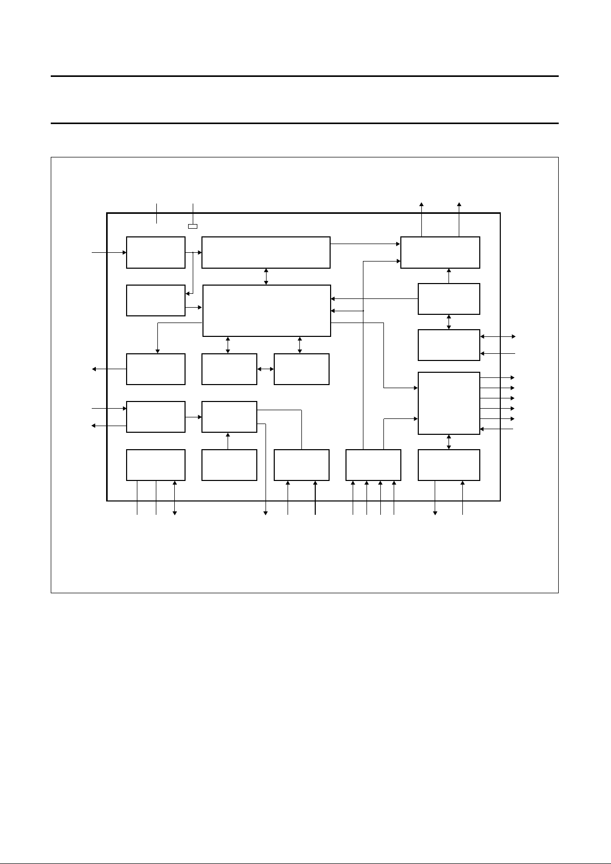
5 BLOCK DIAGRAMS
Fig.1 Block diagram (SO28; SOT136-1).
handbook, full pagewidth
PD
PS
DO DS
PCF5001T
RECEIVER
ENABLE
CONTROL
OSCILLATOR
VOLTAGE
CONVERTER
POWER-ON
RESET
TEST
CONTROL
STATUS
CONTROL
CLOCK
RECOVERY
CLOCK
GENERATION
DATA OUTPUT
CONTROL
DIGITAL INPUT
FILTER
SYNC
CONTROL
TIMING
CONTROL
DECODER AND
ERROR CORRECTION
CONTROL
BL BSSR SK ON IE
EEPROM
MEMORY
EEPROM
CONTROL
ALERT
GENERATION
CONTROL
BATTERY LOW
CONTROL
SERIAL DATA PROCESSOR
26 27
AH
AL
OR
OM
OL
AI
DI
TS TTFLCP CN
RE
X1
X2
12
15
25
16
13
23
V
ref
V
SS
V
DD
5
14
9
10
7
8
17 4
3 2 1 28 11 18 21202219 24 6
MCD454
1997 Mar 04 5
Philips Semiconductors Product specification
POCSAG Paging Decoder PCF5001
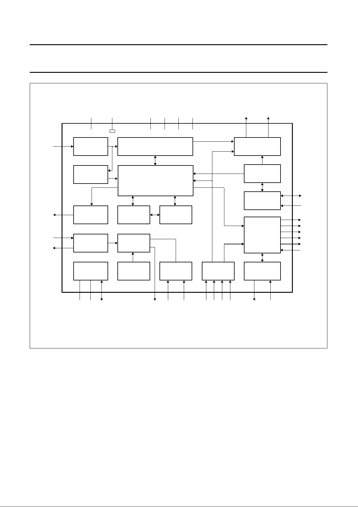
Fig.2 Block diagram (LQFP32; SOT358-1).
handbook, full pagewidth
PD
PS
DO DS
PCF5001H
RECEIVER
ENABLE
CONTROL
OSCILLATOR
VOLTAGE
CONVERTER
POWER-ON
RESET
TEST
CONTROL
STATUS
CONTROL
CLOCK
RECOVERY
CLOCK
GENERATION
DATA OUTPUT
CONTROL
DIGITAL INPUT
FILTER
SYNC
CONTROL
TIMING
CONTROL
DECODER AND
ERROR CORRECTION
CONTROL
BL BSSR SK ON IE
EEPROM
MEMORY
EEPROM
CONTROL
ALERT
GENERATION
CONTROL
BATTERY LOW
CONTROL
SERIAL DATA PROCESSOR
10 11
AH
AL
OR
OM
OL
AI
DI
TS TTFLCP CN
RE
X1
X2
26
29
9
30
27
6
V
ref
V
DD
17
28
23
24
19
22
V
SS
31 16
15 14 13 12 25 32 4 3 5 1 8 18
MLB045
n.c.2n.c.7n.c.20n.c.
21

1997 Mar 04 6
Philips Semiconductors Product specification
POCSAG Paging Decoder PCF5001
6 PINNING
SYMBOL
PIN
DESCRIPTION
PCF5001T
(SOT136-1)
PCF5001H
(SOT358-1)
V
ref
1 13 Microcontroller interface reference voltage input/output. The LOW level of
pins FL, DS, DO, OR, BL, AI, ON, SK, SR and IE is related to the voltage
on V
ref
. May be driven from an external negative voltage source or must
be connected to VSS, if pins CN and CP are left open-circuit. When the
on-chip voltage converter is used, this pin provides a doubled negative
output voltage.
CN 2 14 Voltage converter external shunt capacitance, negative side. Connect the
negative side of the shunt capacitor to this pin, if the on-chip voltage
converter function is used.
CP 3 15 Voltage converter external shunt capacitor, positive side. Connect the
positive side of the shunt capacitor to this pin, if the on-chip voltage
converter function is used.
V
DD
4 16 Main positive power supply. This pin is common to all supply voltages and
is referred to as 0 V (common).
DI 5 17 Serial data input (POCSAG code). The serial data signal train applied to
this pin is processed by the decoder. Pulled LOW by an on-chip pull-down
when the receiver is disabled (RE = LOW).
BS 6 18 Battery-low indication input. The decoder samples this input during
synchronization scan, when it is in ON or SILENT status and the receiver
is enabled (RE = HIGH). A battery-low condition is assumed, if the
decoder detects four consecutive samples HIGH. An audible battery-low
indication is made by the decoder, when operating in ON status. Normally
LOW by the operation of an on-chip pull-down.
PD 7 19 EEPROM programming data input and output. Normally HIGH by the
operation of an on-chip pull-up. During programming of the on-chip
EEPROM, PD is a bidirectional data and control signal.
PS 8 22 EEPROM programming strobe input. Normally LOW by the operation of
an on-chip pull-down. During programming of the on-chip EEPROM, PS is
a unidirectional control input.
X1 9 23 Crystal oscillator input. Connect a 32768 Hz or 76800 Hz crystal and a
biasing resistor between this pin and X2. In addition, provide a load
capacitance to V
DD
, which may also be used for frequency tuning.
X2 10 24 Crystal oscillator output. Return connection for the external crystal and
resistor at X1.
TS 11 25 Scan test mode enable input. Always LOW by operation of an on-chip
pull-down.
AH 12 26 Alert HIGH-level output. This output can directly drive an external bipolar
transistor to control HIGH-level alerting in conjunction with AL, by means
of an alerter or beeper.
OL 13 27 LED indication output. This output can directly drive an external bipolar
transistor to control the visual alert function by means of an LED. It may
also be used for visual indication of received call data during call
reception.

1997 Mar 04 7
Philips Semiconductors Product specification
POCSAG Paging Decoder PCF5001
RE 14 28 Receiver enable output. May be used to control the paging receiver power
control input, to minimize power consumption. The decoder provides a
HIGH-level at this pin, when receiver operation is requested. Each time
the decoder does not require any input data at DI the receiver enable
output is LOW.
AL 15 29 Alert LOW-level output. Open drain alert output in anti-phase to AH, to
provide LOW-level alerting. HIGH-level alerting is generated in conjunction
with AH.
OM 16 30 Vibrator output. This output can directly drive an external bipolar transistor
to control a vibrator type alerter.
V
SS
17 31 Main negative supply voltage.
TT 18 32 Test mode enable input. Always LOW by operation of an on-chip
pull-down.
IE 19 1 Interface enable input. While the interface enable input is active HIGH,
operation of the ON, SK, SR, AI, BL and OR inputs and outputs is
possible. When IE is LOW the inputs do not respond to applied signals
and the outputs are made high-impedance. In alert-only pager mode the
interface enable input does not have any effect on the operation of inputs
ON, SK and SR, but IE must be referenced to LOW or HIGH.
SK 20 3 SILENT state control input. The SILENT control input selects the decoder
ON status (LOW-level) or SILENT status (HIGH-level), if the ON input is
active HIGH. An on-chip pull-up is provided, if the decoder has been
programmed for ‘alert-only pager’ mode, whereby the pull-up is disabled
for display pager mode. In ‘display pager’ mode status change is
possible if the interface enable input (IE) is HIGH and the status is latched
on the falling edge of IE.
SR 21 4 Status request and reset input. A HIGH-going pulse on this input causes
(a) status indication cadence to be generated, if the decoder is not alerting
or (b) resetting of a call alert, repeated call alert or battery-low alert, if
active or (c) triggers the call store re-alert facility, if repeat mode is active.
In ‘display pager’ mode operation of SR is possible only if the interface
control input is active. Normally LOW by the operation of an on-chip
pull-down.
ON 22 5 On/off control input. The on/off control input selects the decoder ON status
(HIGH-level) or OFF status (LOW-level). An on-chip pull-up resistor is
provided, if the decoder has been programmed for ‘alert-only pager’ mode,
but the pull-up resistor is disabled for ‘display pager’ mode. In
‘display pager’ mode, status change is possible if the interface enable
input (IE) is HIGH and the status is latched on the falling edge of IE.
AI 23 6 Alarm input. A HIGH-level on this input causes generation of a continuous
HIGH-level alert via AH and AL outputs, if the decoder operates in ON
status or OFF status. In addition, the LED output is active independent
from the decoder status, but in accordance with AI. Pulsing the input may
be used to modulate the alert and LED indication. Normally LOW in
‘alert-only pager’ mode by operation of an on-chip pull-down.
SYMBOL
PIN
DESCRIPTION
PCF5001T
(SOT136-1)
PCF5001H
(SOT358-1)

1997 Mar 04 8
Philips Semiconductors Product specification
POCSAG Paging Decoder PCF5001
BL 24 8 Battery-low indication output. If the decoder encounters a battery-low
condition a battery-low output latch is set HIGH. The battery-low output
latch may be tested for a battery-low condition, whenever the interface
enable input (IE) is active (HIGH), otherwise the battery-low output is
made high-impedance. The battery-low output latch is reset only, by
switching the decoder to OFF status.
OR 25 9 Out-of-range indication output. Whenever the decoder detects an
out-of-range condition an out-of-range output latch is set HIGH after expiry
of the programmed out-of-range hold-off time selected by means of
special programming (SPF06 and SPF07) of the EEPROM. The
out-of-range latch may be tested for an out-of-range condition, whenever
the interface enable input (IE) is active (HIGH), otherwise the out-of-range
output is made high-impedance. The out-of- range output is reset by
detection of a valid data transmission or by switching the decoder to OFF
status.
DO 26 10 Serial interface data output. During normal decoder operation, accepted
calls and possibly subsequent message data are serially output via this pin
in conjunction with the data strobe output (DS). This pin is also used to
output the EEPROM contents upon special command, if the decoder is
programmed for display pager.
DS 27 1 1 Serial interface data strobe output. Provides a clock signal for the received
call data and EEPROM data appearing at the data output (DO). Each time
this output is LOW the data at DO is valid. Additional start and stop
conditions allow easy identification of data sequence start and end.
FL 28 12 Frequency reference output. When programmed for ‘display pager’ mode,
this output provides a clock reference with 16384 or 32768 Hz per
second, selected by SPF32. See Chapter 7.
n.c. − 2, 7, 20, 21 Not connected.
SYMBOL
PIN
DESCRIPTION
PCF5001T
(SOT136-1)
PCF5001H
(SOT358-1)
1997 Mar 04 9
Philips Semiconductors Product specification
POCSAG Paging Decoder PCF5001
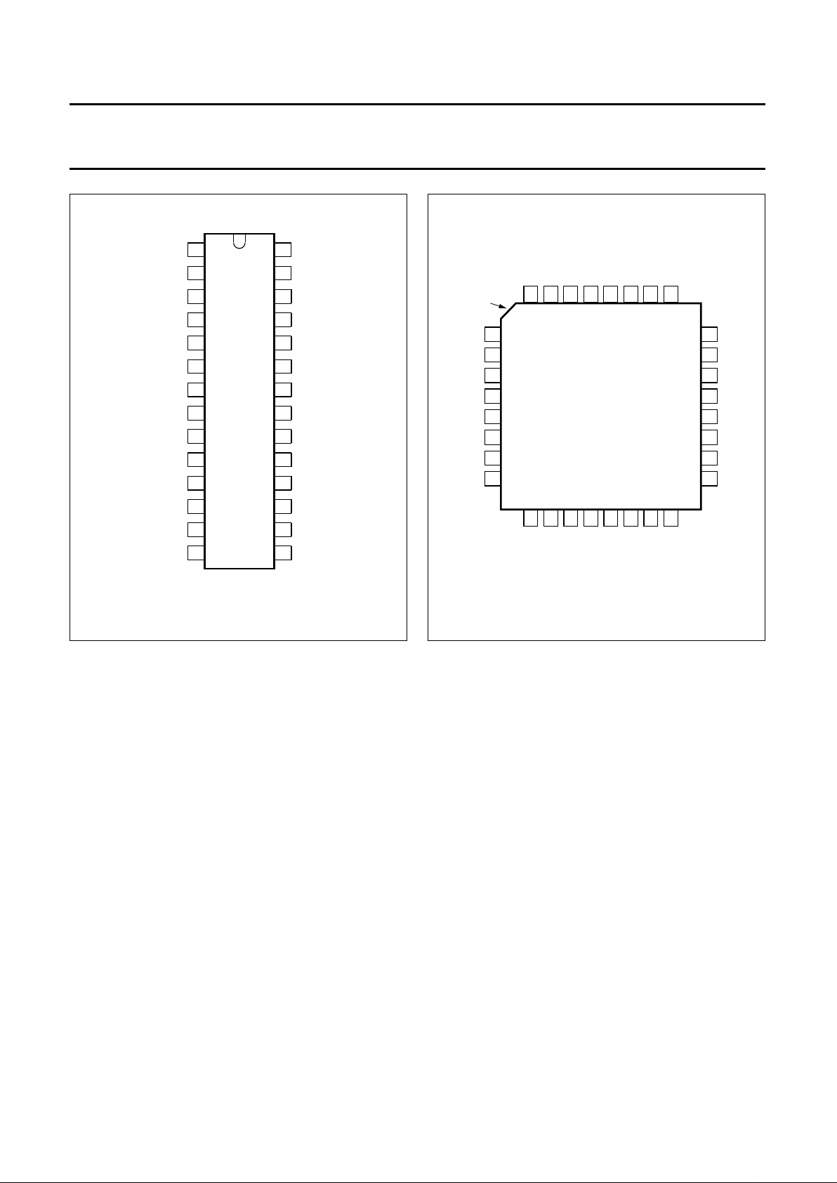
Fig.3 Pin configuration PCF5001T (SOT136-1).
handbook, halfpage
28
27
26
25
24
23
22
21
20
19
18
17
16
15
1
2
3
4
5
6
7
8
9
10
11
12
13
14
MCD455 - 1
DS
DO
OR
BL
AI
ON
SR
SK
IE
TT
OM
AL
FL
PCF5001T
CN
CP
DI
BS
PD
PS
X1
X2
TS
AH
OL
RE
V
ref
V
DD
V
SS
Fig.4 Pin configuration PCF5001H (SOT358-1).
handbook, halfpage
1
2
3
4
5
6
7
8
24
23
22
21
20
19
18
17
9
10
11
12
13
14
15
16
32
31
30
29
28
27
26
25
index
corner
IE
n.c.
SK
SR
ON
AI
n.c.
BL
OR
DO
DS
FL
V
ref
CN
CP
V
DD
DI
BS
PD
n.c.
n.c.
PS
X1
X2
TS
AH
OL
RE
AL
OM
VSSTT
PCF5001H
MLB048
7 FUNCTIONAL DESCRIPTION
The PCF5001 is a very low power Decoder and Pager
Controller specifically designed for use in new generation
radio pagers. The architecture of the PCF5001 allows for
flexible application in a wide variety of radio pager designs.
The PCF5001 is fully compatible with
“CCIR radio paging
Code Number 1”
(also known as the POCSAG code)
operating at the originally specified 512 bits/s data rate,
and also at the newly specified 1200 bits/s data rate
(2400 bits/s operation is also possible). The PCF5001 also
offers features which extend the basic flexibility and
efficiency of this code standard.
7.1 The PCF5001 supports two basic modes of
operation
In alert-only pager mode only a minimum number of
external components are required to build a complete
tone-only pager. Selection of operating states ON, OFF or
SILENT is achieved using a slider switch interface.
In display pager mode the state input logic is switched to
a bus interface structure. Received calls and messages
are transferred to an external microcontroller via the serial
microcontroller interface. A built-in voltage converter with
increased drive capabilities can supply doubled supply
voltage output, and appropriate logic level shifting on
microcontroller interface signals is provided.
Upon reception of valid calls one of eight different call
cadences is generated; upon status interrogation status
indication tones make the current status of the decoder
available to the user.
On-chip non-volatile 114-bit EEPROM storage is provided
to hold up to four user addresses, two frame numbers and
the programmed decoder configuration.
Synchronization to the input data stream is achieved using
the improved ACCESS
algorithm, which allows for data
synchronization and re-synchronization without preamble
detection while minimizing battery power consumption by
receiver power control. One of four error correction
algorithms is applied to the received data to optimize the
call success rate.

1997 Mar 04 10
Philips Semiconductors Product specification
POCSAG Paging Decoder PCF5001
7.2 The POCSAG paging code
A transmission using the
“CCIR Radio paging Code No. 1”
(POCSAG code) is constructed in accordance with the
following rules (see Fig.5).
The transmission is started by sending a preamble,
consisting of at least 576 continuously alternating bits
(10101010...). The preamble is followed by an arbitrary
number of batch blocks. Only complete batches are
transmitted.
Each batch comprises 17 codewords of 32 bits each.
The first codeword is a synchronization codeword with a
fixed pattern. The sync word is followed by 8 frames
(0 to 7) of 2 codewords each, containing message
information. A codeword in a frame can either be an
address, message or idle codeword.
Idle codewords also have a fixed pattern and are used to
fill empty frames or to separate messages.
Address codewords are identified by an MSB at logic 0
and are coded as shown in Fig.5. A user address or RIC
consists of 21 bits. Only the upper 18 bits are encoded in
the address codeword (bits 2 to 19). The lower 3 bits
designate the frame number (0 to 7) in which the address
is transmitted.
Four different call types (‘numeric’, ‘alphanumeric’ and two
‘alert only’ types) can be distinguished. The call type is
determined by two function bits in the address codeword
(bits 20 and 21).
Alert-only calls consist only of a single address codeword.
Numeric and alphanumeric calls have message
codewords following the address. A message causes the
frame structure to be temporarily suspended. Message
codewords are sent until the message is completed, with
only the sync words being transmitted in their expected
positions.
Message codewords are identified by an MSB at logic 1
and are coded as shown in Fig.5. The message
information is stored in a 20-bit field (bits 2 to 21).
The standard data format is determined by the call type: 4
bits per digit for numeric messages and 7 bits per (ASCII)
character for alphanumeric messages.
Each codeword is protected against transmission errors by
10 CRC check bits (bits 22 to 31) and an even-parity bit
(bit 32). This permits correction of a maximum of 2 random
errors or up to 3 errors in a burst of 4 bits (a 4-bit burst
error) per codeword.
Fig.5 POCSAG code structure.
handbook, full pagewidth
PREAMBLE BATCH 1 BATCH 2 BATCH 3 LAST BATCH
SYNC | CW CW | CW CW | . . . . . | CW CW
FRAME 0 FRAME 1 FRAME 7
10101 . . . 10101010
Address code-word
Message code-word
0 18-bit address 2 function bits 10 CRC bits P
1 20-bit message 10 CRC bits P
MCD456

1997 Mar 04 11
Philips Semiconductors Product specification
POCSAG Paging Decoder PCF5001
7.3 Modes and states of the decoder
The PCF5001 supports two basic operating modes:
• ‘Alert-only pager’ mode
• ‘Display pager’ mode.
Two further modes, the programming mode and the test
mode, are implemented to program and verify the
EEPROM contents and to support pager production and
approval tests, respectively.
In ‘alert-only pager’ mode no external microcontroller is
required, see Fig.22. A three position slider switch
interface is provided to select the internal state of the
decoder. The decoder performs regular scanning of the
switch inputs to detect a status change. A push-button
interface is provided on the SR input, which is used as
input for user acknowledgment actions and status
interrogation. Upon reception of valid calls, tone alert
cadences are generated. A call storage is provided to store
calls received while operating in SILENT status and to
recall cadences upon ‘repeat’ mode operation.
The voltage doubler and the frequency reference output
are disabled in this mode.
In ‘display pager’ mode the PCF5001 operates as decoder
and pager controller in combination with an external
microcontroller (see Fig.23). The internal states of the
decoder are determined by appropriate logic levels on the
status inputs. A bus type interface structure is used to
interface the decoder to the microcontroller. The decoder's
on-chip voltage converter provides doubled supply voltage
output to provide a higher supply voltage to the
microcontroller and any additional hardware. The logic
levels of the interface's input and output signals are level
shifted to allow for direct coupling between microcontroller
and the decoder. Upon detection of a valid call, address
and message information are transferred to the external
microcontroller using the serial microcontroller interface.
In addition, appropriate call alert cadences are generated.
If the decoder is in one of the two operating modes, it is
always in one of the following three internal states:
• OFF status. This is the power saving, inactive status of
the PCF5001. The paging receiver is disabled, no
decoding of input data takes place. However, the crystal
oscillator is kept running to ensure that scanning of the
status inputs/status switch is maintained to allow
changing into one of the following two active states.
• ON status. This is the normal active status of the
decoder. Incoming calls are compared with the user
addresses stored in the internal EEPROM. Upon
detection of valid calls, alert cadences and LED
indication are generated and data is shifted out at the
serial microcontroller interface.
• SILENT status. The SILENT status is the same as the
ON status with the exception that valid calls no longer
cause generation of call alert cadences. Instead, if
programmed as ‘alert-only pager’, the decoder stores up
to eight different calls and generates appropriate alert
cadences after the decoder has been put back into the
ON status. However, special SILENT override calls will
cause generation of alert cadences, if enabled.
The decoder operating status is selected as indicated in
Table 1.
When programmed for ‘alert-only pager’ a switch
debounce period is applied to the status inputs. For status
change and status interrogation in ‘display pager’ mode,
see Figs 6 and 7.
Table 1 Truth table for decoder operating status
Note
1. The EEPROM transfer mode applies to ‘display pager’ mode only.
ON INPUT SK INPUT OPERATING STATUS
0 0 OFF
0 1 OFF (EEPROM transfer mode; note 1)
10ON
1 1 SILENT

1997 Mar 04 12
Philips Semiconductors Product specification
POCSAG Paging Decoder PCF5001
Fig.6 Status change in display pager mode.
INTERNAL
STATUS
IE
ON
SK
tt t
STP STD STD
t
IEH
t
STH
MCD457 - 1
Fig.7 Status interrogation in display pager mode.
MCD458
IE
SR
tt t t t
STP STH SPD IEH STH
7.4 Decoding of the POCSAG data stream
The POCSAG coded input data stream is first noise filtered
by a digital filter. From the filtered data a sampling clock
synchronous to the data rate is derived. The PCF5001
supports 512 bits/s and 1200 bits/s data rates. This results
in a 512 Hz or 1200 Hz sampling clock frequency,
respectively. Synchronization on the POCSAG code
structure is performed using the improved Philips
ACCESS algorithm, which employs a state machine with
six internal states.
A data rate of 2400 bits/s is possible if an external clock
generator of 153.6 kHz is connected to X1. The minimum
supply voltage is then −1.8 V.
The receiver enable output is activated a period equal to
t
RXON
before the input data is actually needed. The
decoder has first to achieve bit and word synchronization
before it can receive calls. The algorithm searches first for
the preamble and then for synchronization codeword
patterns.

1997 Mar 04 13
Philips Semiconductors Product specification
POCSAG Paging Decoder PCF5001
This is carried out for the duration of 3 batches in
power-on mode or 1 batch (=preamble duration) in
preamble receive mode. Error correction algorithms are
applied to the data before it is compared with preamble
and synchronization codeword patterns.
The synchronization process is terminated and thus
data receive mode is entered as soon as synchronization
codewords are seen at the beginning of each batch.
The decoder handles loss of synchronization in three
steps:
1. If the decoder fails to detect the synchronization
pattern at the beginning of the current batch it
continues data reception as normal. This data fail
mode is signalled in the message output when an
address codeword was received, as shown in Table 4.
2. If also at the beginning of the next batch no
synchronization codeword can be detected, the
algorithm assumes a small bit shift in the
fade recovery mode and performs more
synchronization codeword checks around the
expected position for the following 15 batches. Call
reception is suspended.
3. If it fails to re-synchronize in the ‘fade recovery’ mode,
the carrier off mode is selected, in which the decoder
attempts to regain synchronization by bit-wise shifting
its synchronization scan window. Using this technique
re-synchronization is obtained within a continuous
data stream of at least 18 batches without preamble
detection.
In ‘data receive’ mode, the input data stream is sampled at
the synchronization codeword position and the
programmed frame positions. The received codewords are
error corrected and then, if address codewords, compared
with the stored user addresses related to that frame.
On detection of a valid call, the decoder performs the
following three operations:
1. Set a store for call alert cadence generation according
to the combination of the function bits in the accepted
address codeword. The call alert cadence will not be
generated before the call has been terminated.
2. Keep the receiver enable output (RE) active and
receive subsequent message codewords, until any of
the call termination criteria are fulfilled.
3. Trigger the serial message transfer by sending a start
condition and transfer deformatted message
codewords as attached to the address codeword via
the serial microcontroller interface to an external
microcontroller, followed by a stop condition.
Normally call termination is assumed, when a valid idle or
address codeword is received. On reception of
uncorrectable codewords, call termination takes place in
accordance with conditions shown in Table 2.
Table 2 Call termination on error
Note
1. X = don’t care.
SPF12 SPF13 CALL TERMINATION EVENT
0X
(1)
Any two consecutive codewords or the codeword directly following the address
codeword uncorrectable.
1 0 Any single codeword uncorrectable.
1 1 Any two consecutive codewords uncorrectable.

1997 Mar 04 14
Philips Semiconductors Product specification
POCSAG Paging Decoder PCF5001
7.5 Generation of output signals
The PCF5001 provides output indications for call alert,
repeat mode alert, out of range alert, battery-low alert,
status indication alert and start-up alert. Some of the alert
functions may be freely configured by programming of
SPF bits within the EEPROM.
Table 3 shows the outputs which are used for special
output indications, if the decoder operates in ON status.
Remark: reception of special SILENT override calls
causes the decoder to generate call alert indication via AL
and AH even if it operates in SILENT status.
Table 3 Output signals
Note
1. Entries in parenthesis are not valid, if the decoder operates in SILENT status.
ALERT FUNCTION
OUTPUT ACTIVE
(1)
AL AH OL OM OR BL
Start-up (yes) − yes yes −−
Status indication yes −−−−−
Call reception (yes) (yes) yes SPF11 −−
Repeat mode (SPF16) (SPF16) SPF16 −−−
Out-of-range −−SPF15 − yes −
Battery-low (yes) (yes) −−−yes
Alarm input (yes) (yes) yes −−−
7.6 Alerter
The PCF5001 provides the AL and AH outputs for
acoustical LOW-level and HIGH-level signalling.
LOW-level alerting is provided by the AL output only.
For HIGH-level alerting both, AL and AH are active in
anti-phase. The square-wave output signals produce tone
alert cadences by means of a magnetic or piezo ceramic
beeper. The alert frequency, 2048 Hz or 2731 Hz
square-wave, is selected by programming of SPF31.
When valid calls are received while operating in ON status,
the PCF5001 generates call alert cadences. The first four
seconds are generated at LOW-level, a further twelve
seconds are generated at HIGH-level. Alert tone
generation and LED indication automatically terminate
after sixteen seconds unless terminated by pulsing the
status request and reset input (SR). Call alert generation
is inhibited until completion of message codeword
reception and the termination word is sent by the decoder.
Call alert generation commences after an alert delay
period, t
ALD
, at the earliest, see Fig.8. Call alert deletion is
possible during the alert delay period.
The call alert cadence is modulated according to the two
function bits (FC) in the received address codeword,
see Fig.9.
Valid calls received on RIC B or RIC D cause the alerter
frequency to be warbled by means of an additional 16 Hz
and 1024 Hz signal (respective 1365 Hz for SPF31 = 1)
as opposed to RIC A and RIC C where no alert frequency
warble takes place. Thus, eight different call cadences are
distinguishable.
ON status interrogation by the status request and reset
input (SR) the PCF5001 generates a status cadence at
LOW-level, in accordance with the present internal
decoder status (see Fig.10).
When detecting a battery-low condition the PCF5001
provides a battery-low indication. Operating in ON status
causes generation of a battery-low alert at HIGH-level for
sixteen seconds or until terminated by pulsing SR.
Operating in SILENT status or ‘repeat’ mode the
battery-low alert is stored and inhibited until switching to
ON status.
 Loading...