


DATA SH EET
Product specification
File under Integrated Circuits, IC12
1998 May 11
INTEGRATED CIRCUITS
PCF2103 family
LCD controllers/drivers

1998 May 11 2
Philips Semiconductors Product specification
LCD controllers/drivers PCF2103 family
CONTENTS
1 FEATURES
2 APPLICATIONS
3 GENERAL DESCRIPTION
4 ORDERING INFORMATION
5 BLOCK DIAGRAM
6 PINNING
7 FUNCTIONAL DESCRIPTION
7.1 LCD bias voltage generator
7.2 Oscillator
7.3 External clock
7.4 Power-on reset
7.5 Power-down mode
7.6 Registers
7.7 Busy flag
7.8 Address Counter (AC)
7.9 Display Data RAM (DDRAM)
7.10 Character Generator ROM (CGROM)
7.11 Character Generator RAM (CGRAM)
7.12 Cursor control circuit
7.13 Timing generator
7.14 LCD row and column drivers
7.15 Reset function
8 INSTRUCTIONS
8.1 Clear display
8.2 Return home
8.3 Entry mode set
8.3.1 I/D
8.3.2 S
8.4 Display control (and partial power-down mode)
8.4.1 D
8.4.2 C
8.4.3 B
8.5 Cursor or display shift
8.6 Function set
8.6.1 DL (parallel mode only)
8.6.2 M
8.6.3 H
8.7 Set CGRAM address
8.8 Set DDRAM address
8.9 Read busy flag and address counter
8.10 Write data to CGRAM or DDRAM
8.11 Read data from CGRAM or DDRAM
8.12 Extended function set instructions and features
8.12.1 New instructions
8.12.2 Icon control
8.12.3 IM
8.12.4 IB
8.12.5 Screen configuration
8.12.6 Display configuration
8.12.7 Reducing current consumption
9 INTERFACE TO MICROCONTROLLER
9.1 Parallel interface
9.2 I2C-bus interface
9.2.1 Characteristics of the I2C-bus
9.2.2 I2C-bus protocol
9.2.3 Definitions
10 LIMITING VALUES
11 HANDLING
12 DC CHARACTERISTICS
13 AC CHARACTERISTICS
14 TIMING CHARACTERISTICS
15 APPLICATION INFORMATION
15.1 8-bit operation, 1-line display using internal
reset
15.2 4-bit operation, 1-line display using internal
reset
15.3 8-bit operation, 2-line display
15.4 I2C-bus operation, 1-line display
16 BONDING PAD LOCATIONS
17 DEFINITIONS
18 LIFE SUPPORT APPLICATIONS
19 PURCHASE OF PHILIPS I2C COMPONENTS

1998 May 11 3
Philips Semiconductors Product specification
LCD controllers/drivers PCF2103 family
2 APPLICATIONS
• Telecom equipment
• Portable instruments
• Point-of-sale terminals.
3 GENERAL DESCRIPTION
The PCF2103 family is a low power CMOS LCD controller
and driver, designed to drive a dot matrix LCD display of
2 line by 12 or 1 line by 24 characters with 5 × 8 dot
format. All necessary functions for the display are provided
in a single chip, including on-chip generation of LCD bias
voltages, resulting in a minimum of external components
and lower system current consumption. The PCF2103
interfaces to most microcontrollers via a 4 or 8-bit bus or
via the 2-wire I
2
C-bus. The chip contains a character
generator and displays alphanumeric and kana
(Japanese) characters. The letter ‘X’ in PCF2103X
characterizes the built-in character set. Various character
sets can be manufactured on request.
4 ORDERING INFORMATION
TYPE NUMBER
PACKAGE
NAME DESCRIPTION VERSION
PCF2103EU/2/F2 − chip with bumps in tray −
1 FEATURES
• Single-chip LCD controller/driver
• 2-line display of up to 12 characters + 120 icons,
or 1-line display of up to 24 characters + 120 icons
• 5 × 7 character format plus cursor; 5 × 8 for kana
(Japanese syllabary) and user defined symbols
• Icon mode: reduced current consumption while
displaying icons only
(1)
• Icon blink function
• On-chip:
– Generation of intermediate LCD bias voltages
– Oscillator requires no external components
(external clock also possible)
• Display data RAM: 80 characters
• Character generator ROM: 240, 5 × 8 characters
• Character generator RAM: 16, 5 × 8 characters;
3 characters used to drive 120 icons, 6 characters used
if icon blink feature is used in application
• 4 or 8-bit parallel bus and 2-wire I
2
C-bus interface
• CMOS compatible
• 18 row, 60 column outputs
• Mux rates 1 : 18 (for normal operation) and 1 : 2
(for icon-only mode)
• Uses common 11 code instruction set (extended)
• Logic supply voltage range, VDD− VSS= 1.8 to 5.5 V;
chip may be driven with two battery cells
• Display supply voltage range, V
LCD
− VSS= 2.2 to 6.5 V
• Very low current consumption (20 to 120 µA):
– Icon mode: <25 µA
– Power-down mode: <2.5 µA.
(1) Icon mode is used to save current. When only icons
are displayed, a much lower operating voltage V
LCD
can be used and the switching frequency of the LCD
outputs is reduced. In most applications it is possible
to use VDD as V
LCD
.
1998 May 11 4
Philips Semiconductors Product specification
LCD controllers/drivers PCF2103 family
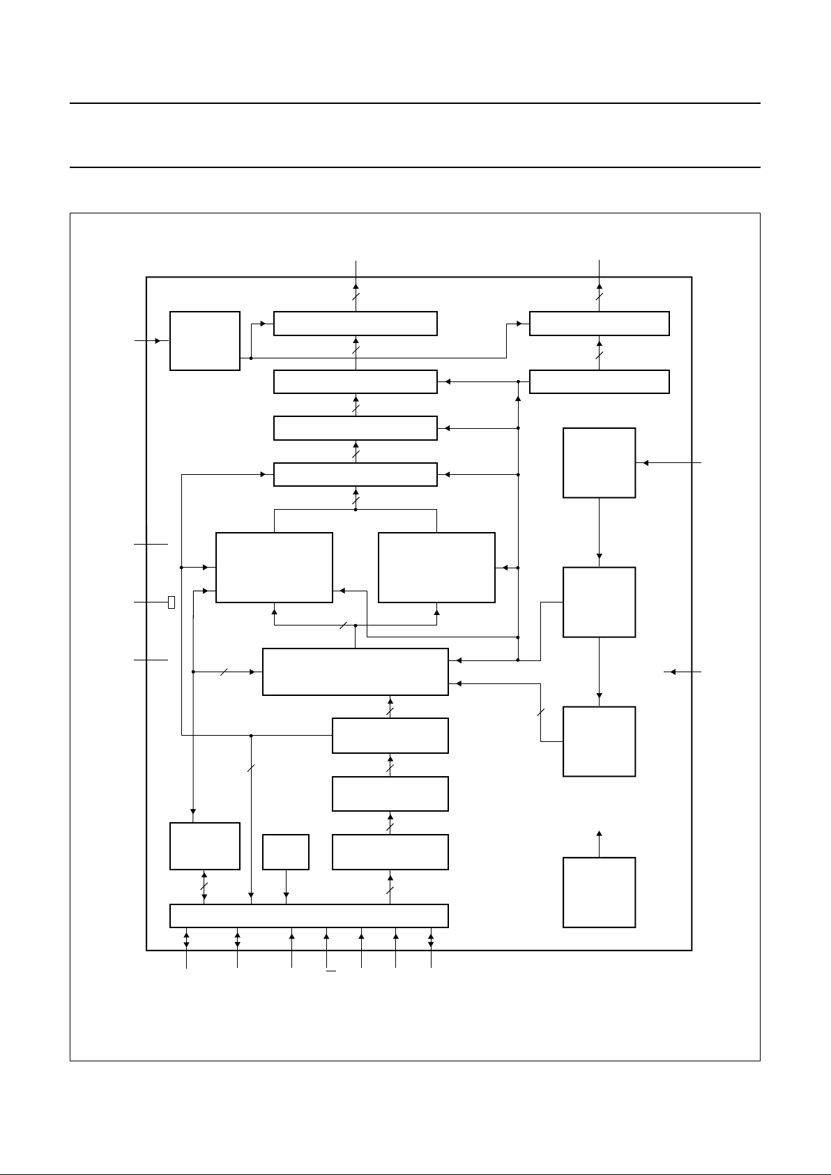
5 BLOCK DIAGRAM
Fig.1 Block diagram.
handbook, full pagewidth
MGL259
CURSOR AND DATA CONTROL
SHIFT REGISTER 5 × 12-BIT
DATA LATCHES
COLUMN DRIVERS
60
5
60
CHARACTER
GENERATOR
RAM (128 × 5)
(CGRAM)
16 CHARACTERS
CHARACTER
GENERATOR
ROM
(CGROM)
240 CHARACTERS
DISPLAY DATA RAM
(DDRAM)
80 CHARACTERS/BYTES
ADDRESS COUNTER
(AC)
INSTRUCTION
DECODER
INSTRUCTION
REGISTER
ROW DRIVERS
SHIFT REGISTER 18-BIT
BIAS
VOLTAGE
GENERATOR
BUSY
FLAG
DATA
REGISTER
(DR)
I/O BUFFER
OSCILLATOR
TIMING
GENERATOR
DISPLAY
ADDRESS
COUNTER
POWER-ON
RESET
V
DD
V
SS
T1
V
LCD
C1 to C60 R1 to R18
OSC
PD
PCF2103
DB0 to DB3/SA0
DB4 to DB7
E
R/W
RS
SCL
SDA
18
18
60
5
7
7
8
8
77
8
8
8
1998 May 11 5
Philips Semiconductors Product specification
LCD controllers/drivers PCF2103 family
6 PINNING
Note
1. This is the voltage used for the generation of LCD bias levels.
SYMBOL DIE PAD DESCRIPTION
V
DD
1 supply voltage
OSC 2 oscillator/external clock input
PD 3 power-down pad input
T1 4 test pad (connected to V
SS
)
V
SS
5 ground
V
LCD
6V
LCD
input; note 1
R9 to R16 7 to 14 LCD row driver outputs 9 to 16
R18 15 LCD row driver output 18
C60 to C1 16 to 23, 26 to 50,
53 to 77, 80, 81
LCD column driver outputs 60 to 1
R8 to R1 82 to 89 LCD row driver outputs 8 to 1
R17 90 LCD row driver output 17
SCL 91 I
2
C-bus serial clock input
SDA 92 I
2
C-bus serial data input/output
E 93 data bus clock input
RS 94 register select input
R/
W 95 read/write input
DB7 96 bit of bi-directional data bus
DB6 97 bit of bi-directional data bus
DB5 98 bit of bi-directional data bus
DB4 99 bit of bi-directional data bus
DB3/SA0 100 bit of bi-directional data bus/I
2
C-bus address pin
DB2 101 bit of bi-directional data bus
DB1 102 bit of bi-directional data bus
DB0 103 bit of bi-directional data bus
1998 May 11 6
Philips Semiconductors Product specification
LCD controllers/drivers PCF2103 family
Table 1 Pin functions; note 1
Note
1. When the I
2
C-bus is used, the parallel interface pin E must be defined as E = 0. In I2C-bus read mode DB7 to DB0
should be connected to VDD or left open-circuit.
a) When the parallel bus is used, pins SCL and SDA must be connected to VSS or VDD; they may not be left
unconnected.
b) If the 4-bit interface is used without reading out from the PCF2103 (i.e. R/W is set permanently to logic 0), the
unused ports DB0 to DB3 can either be set to VSS or VDD instead of leaving them open.
NAME FUNCTION DESCRIPTION
RS register select RS selects the register to be accessed for read and write; there is an internal pull-up
on this pin
RS = 0 selects the instruction register for write and the busy flag and address
counter for read
RS = 1 selects the data register for both read and write
R/
W read/write R/W selects either the read (R/W = 1) or write (R/W = 0) operation; there is an
internal pull-up on this pin
E data bus clock pin E is set HIGH to signal the start of a read or write operation; data is clocked in or
out of the chip on the negative edge of the clock
DB7 to DB0 data bus the bi-directional, 3-state data bus transfers data between the system controller and
the PCF2103; DB7 may be used as the busy flag, signalling that internal operations
are not yet completed; in 4-bit operations the 4 higher order lines DB7 to DB4 are
used; DB3 to DB0 must be left open-circuit; there is an internal pull-up on each of the
data lines
C1 to C60 column driver
outputs
these pins output the data for columns
R1 to R18 row driver
outputs
these pins output the row select waveforms to the display; R17 and R18 drive the
icons
V
LCD
LCD power
supply
positive power supply for the liquid crystal display
OSC oscillator when the on-chip oscillator is used this pin must be connected to V
DD
; an external
clock signal, if used, is input at this pin
SCL serial clock line input for the I
2
C-bus clock signal
SDA serial data line I/O for the I
2
C-bus data line
SA0 address pin the hardware sub-address line is used to program the device sub-address for two
different PCF2103s on the same I
2
C-bus
T1 test pad must be connected to V
SS
; not user accessible
PD power-down pad PD selects chip power-down mode; for normal operation PD = 0
1998 May 11 7
Philips Semiconductors Product specification
LCD controllers/drivers PCF2103 family
7 FUNCTIONAL DESCRIPTION
7.1 LCD bias voltage generator
The intermediate bias voltages for the LCD display are generated on-chip. This removes the need for an external
resistive bias chain and significantly reduces the system current consumption. The optimum value of V
LCD
depends on
the multiplex rate, the LCD threshold voltage (Vth) and the number of bias levels and is given by the relationships given
in Tables 2 and 3. Using a 5-level bias scheme for 1 : 18 maximum rate allows V
LCD
<5 V for most LCD liquids.
Table 2 Optimum/maximum values for V
OP
(off pixels start darkening; V
off=Vth
)
Table 3 Minimum values for V
OP
(on pixels clearly visible; Von>Vth)
MUX RATE NUMBER OF LEVELS V
on/Vth
VOP/V
th
VOP(typical; for Vth= 1.4 V)
1 : 18 5 1.272 3.7 5.2 V
1 : 2 3 2.236 2.283 3.9 V
MUX RATE NUMBER OF LEVELS V
on/Vth
VOP/V
th
VOP(typical; for Vth= 1.4 V)
1 : 18 5 1.12 3.2 4.6 V
1 : 2 3 1.2 1.5 2.1 V
7.2 Oscillator
The on-chip oscillator provides the clock signal for the
display system. No external components are required and
pin OSC must be connected to VDD.
7.3 External clock
If an external clock is to be used, it is input at the OSC pin.
The resulting display frame frequency is given by
Only in the power-down state is the clock allowed to be
stopped (OSC connected to V
SS
), otherwise the LCD is
frozen in a DC state.
7.4 Power-on reset
The on-chip power-on reset block initializes the chip after
power-on or power failure. This is a synchronous reset and
requires 3 oscillator cycles to be executed. Afterwards, a
clear display is initiated.
7.5 Power-down mode
The chip can be put into power-down mode where all static
currents are switched off (no internal oscillator, no bias
level generation, all LCD outputs are internally connected
to V
SS
) when PD = 1.
f
frame
f
osc
3072
------------ -
=
During power-down, the whole chip is being reset and will
restart with a clear display after power-down. Therefore,
the whole chip has to be initialized after a power-down as
after an initial power-up.
7.6 Registers
The PCF2103 has two 8-bit registers, an Instruction
Register (IR) and a Data Register (DR). The Register
Select signal (RS) determines which register will be
accessed. The instruction register stores instruction codes
such as ‘display clear’ and ‘cursor shift’, and address
information for the Display Data RAM (DDRAM) and
Character Generator RAM (CGRAM). The instruction
register can be written from but not read by the system
controller. The data register temporarily stores data to be
read from the DDRAM and CGRAM. When reading, data
from the DDRAM or CGRAM corresponding to the address
in the instruction register is written to the data register prior
to being read by the ‘read data’ instruction.
7.7 Busy flag
The busy flag indicates the internal status of the PCF2103.
Logic 1 indicates that the chip is busy and further
instructions will not be accepted. The busy flag is output at
pin DB7 when RS = 0 and R/
W = 1. Instructions should
only be written after checking that the busy flag is logic 0
or waiting for the required number of cycles.
1998 May 11 8
Philips Semiconductors Product specification
LCD controllers/drivers PCF2103 family
7.8 Address Counter (AC)
The address counter assigns addresses to the DDRAM
and CGRAM for reading and writing and is set by the
commands ‘set CGRAM address’ and ‘set DDRAM
address’. After a read/write operation the address counter
is automatically incremented or decremented by 1.
The address counter contents are output to the bus
(DB6 to DB0) when RS = 0 and R/W=1.
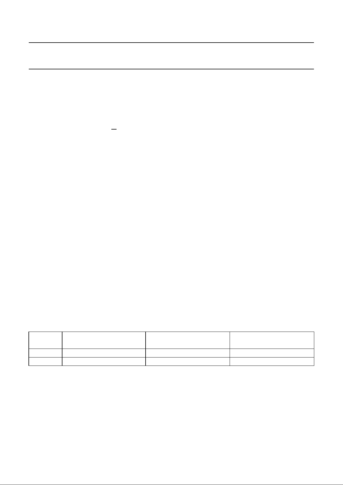
7.9 Display Data RAM (DDRAM)
The DDRAM stores up to 80 characters of display data
represented by 8-bit character codes. RAM locations
which are not used for storing display data can be used as
general purpose RAM. The basic RAM-to-display
addressing scheme is shown in Fig.2. With no display shift
the characters represented by the codes in the first
24 RAM locations starting at address 00 in line 1 are
displayed. Figures 3 and 4 show the display mapping for
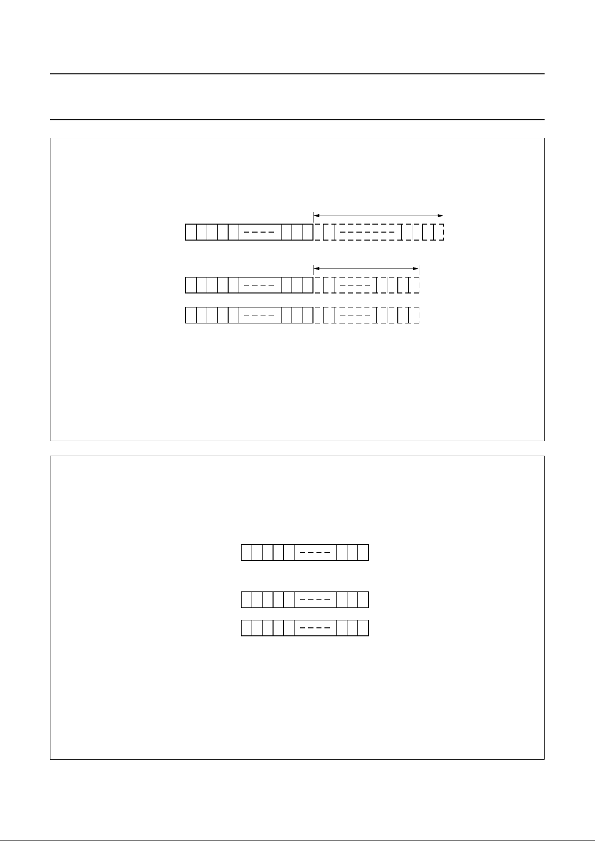
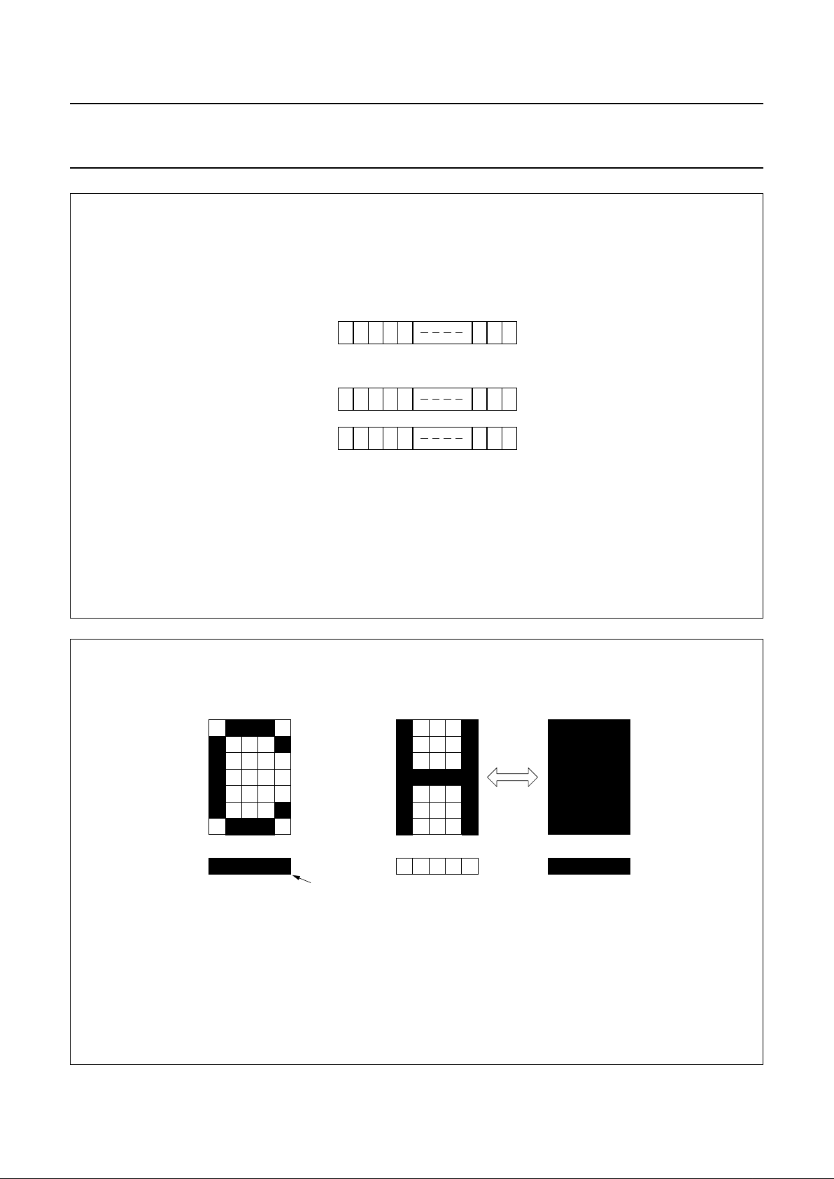
right and left shift respectively.
When data is written to or read from the DDRAM
wrap-around occurs from the end of one line to the start of
the next line. When the display is shifted each line wraps
around within itself, independently of the others. Thus all
lines are shifted and wrapped around together.
The address ranges and wrap-around operations for the
various modes are shown in Table 4.
7.10 Character Generator ROM (CGROM)
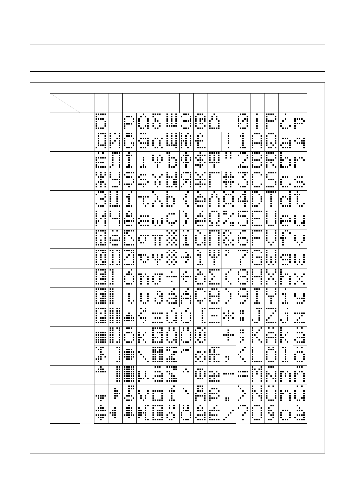
The Character Generator ROM (CGROM) generates
240 character patterns in 5 × 8 dot format from 8-bit
character codes. Figure 6 shows the character set that is
currently implemented.
7.11 Character Generator RAM (CGRAM)
Up to 16 user defined characters may be stored in the
CGRAM. Some CGRAM characters (see Fig.14) are also
used to drive icons (6 if icons blink and both icon rows are
used in application; 3 if no blink but both icon rows are
used in application; 0 if no icons are driven by the icon
rows). The CGROM and CGRAM use a common address
space, of which the first column is reserved for the
CGRAM (see Fig.6). Figure 7 shows the addressing
principle for the CGRAM.
7.12 Cursor control circuit
The cursor control circuit generates the cursor (underline
and/or cursor blink as shown in Fig.5) at the DDRAM
address contained in the address counter. When the
address counter contains the CGRAM address the cursor
will be inhibited.
7.13 Timing generator
The timing generator produces the various signals
required to drive the internal circuitry. Internal chip
operation is not disturbed by operations on the data buses.
7.14 LCD row and column drivers
The PCF2103 contains 18 row and 60 column drivers,
which connect the appropriate LCD bias voltages in
sequence to the display in accordance with the data to be
displayed. R17 and R18 drive the icon rows.
The bias voltages and the timing are selected
automatically when the number of lines in the display is
selected. Figures 8, 9 and 10 show typical waveforms.
Unused outputs should be left unconnected.
Table 4 Address space and wrap-around operation
Notes
1. Moves to next line.
2. Stays within line.
MODE ADDRESS SPACE
READ/WRITE
WRAP-AROUND
(1)
DISPLAY SHIFT
WRAP-AROUND
(2)
1 × 24 00H to 4FH 4FH to 00H 4FH to 00H
2 × 12 00H to 27H; 40H to 67H 27H to 40H; 67H to 00H 27H to 00H; 67H to 40H
1998 May 11 9
Philips Semiconductors Product specification
LCD controllers/drivers PCF2103 family
Fig.2 DDRAM-to-display mapping: no shift.
handbook, full pagewidth
00 01 02 03 04 15 16 17 18 19 4C 4D 4E 4F
non-displayed DDRAM addresses
64 65 66 6740 41 42 43 44 49 4A 4B 4C 4D
00 01 02 03 04 09 0A 0B 0C 0D 24 25 26 27
non-displayed DDRAM address
line 1
line 2
MGE991
DDRAM
address
2-line display
12345 222324
12345 101112
12345 101112
display
position
DDRAM
address
1-line display
Fig.3 DDRAM-to-display mapping: right shift.
handbook, halfpage
MGE992
27 00 01 02 03
67 40 41 42 43
08 09 0A
48 49 4A
DDRAM
address
line 1
line 2
2-line display
1 2 3 4 5 22 23 24
1 2 3 4 5 10 11 12
1 2 3 4 5 10 11 12
4F 00 01 02 03 14 15 16
display
position
DDRAM
address
1-line display
1998 May 11 10
Philips Semiconductors Product specification
LCD controllers/drivers PCF2103 family
Fig.4 DDRAM-to-display mapping: left shift.
handbook, halfpage
01 04 05
41 42 43 44 45
0A 0B 0C
4A 4B 4C
DDRAM
address
line 1
line 2
2-line display
1 2 3 4 5 22 23 24
1 2 3 4 5 10 11 12
1 2 3 4 5 10 11 12
01 04 05
02 03
02 03 16 17 18
display
position
DDRAM
address
1-line display
MGE993
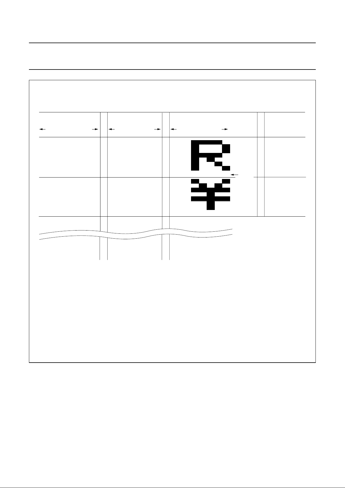
Fig.5 Cursor and blink display examples.
MGA801
cursor
5 x 7 dot character font alternating display
cursor display example blink display example
1998 May 11 11
Philips Semiconductors Product specification
LCD controllers/drivers PCF2103 family
Fig.6 Character set ‘E’ in CGROM.
handbook, full pagewidth
MGD689
0000 0001 0010 0011 0100 0101 0110 0111 1000 1001 1010 1011 1100 1101 1110 1111
upper
4 bits
lower
4 bits
xxxx 0000
xxxx 0001
xxxx 0010
xxxx 0011
xxxx 0100
xxxx 0101
xxxx 0110
xxxx 0111
xxxx 1000
xxxx 1001
xxxx 1010
xxxx 1011
xxxx 1100
xxxx 1101
xxxx 1110
xxxx 1111 16
15
14
13
12
11
10
9
8
7
6
5
4
3
2
1
1998 May 11 12
Philips Semiconductors Product specification
LCD controllers/drivers PCF2103 family
Fig.7 Relationship between CGRAM addresses and data and display patterns.
Character code bits 0to 3 correspond to CGRAM address bits 3 to 6.
CGRAM address bits 0 to 2 designate the character pattern line position. The 8th line is the cursor position and display is performed by logical OR with
the cursor. Data in the 8th position will appear in the cursor position.
Character pattern column positions correspond to CGRAM data bits 0 to 4, as shown in Fig.6.
As shown in Figs 6 and 7, CGRAM character patterns are selected when character code bits 4 to 7 are all logic 0. CGRAM data = logic 1 corresponds
to selection for display.
Only bits 0 to 5 of the CGRAM address are set by the ‘set CGRAM address’ command. Bit 6 can be set using the ‘set DDRAM address’ command in
the valid address range or by using the auto-increment feature during CGRAM write. All bits 0 to6 can be read using the ‘read busy flag and address
counter’ command; see Table 7.
handbook, full pagewidth
MGE995
76543210 6543210 43210
higher
order
bits
lower
order
bits
lower
order
bits
higher
order
bits
lower
order
bits
higher
order
bits
00000000 0000000 0
001 000
010 000
011 0
100 0 00
101 00 0
110 000
111 00000
000 000
001 0 0 0
010
00 00011
100
101 00 00
110 00 00
111 00000
001
00000001 0001
00000010
00001111
00001111
00001111
00001111
010 0000
100
101
110
1
1
1
1
1
1
1
1
1
1
1
1
1
1
1
1
111
character codes
(DDRAM data)
CGRAM
address
character patterns
(CGRAM data)
43210
0
000
111
000
0
0010
00 01
000
1
1
1
00
1
1
1
1111
1
1
1
000
1
101
000
111
0
1111
01 00
010
0
1
0
00
0
1
1
0100
1
0
0
000
character code
(CGRAM data)
character
pattern
example 1
cursor
position
character
pattern
example 2
1998 May 11 13
Philips Semiconductors Product specification
LCD controllers/drivers PCF2103 family
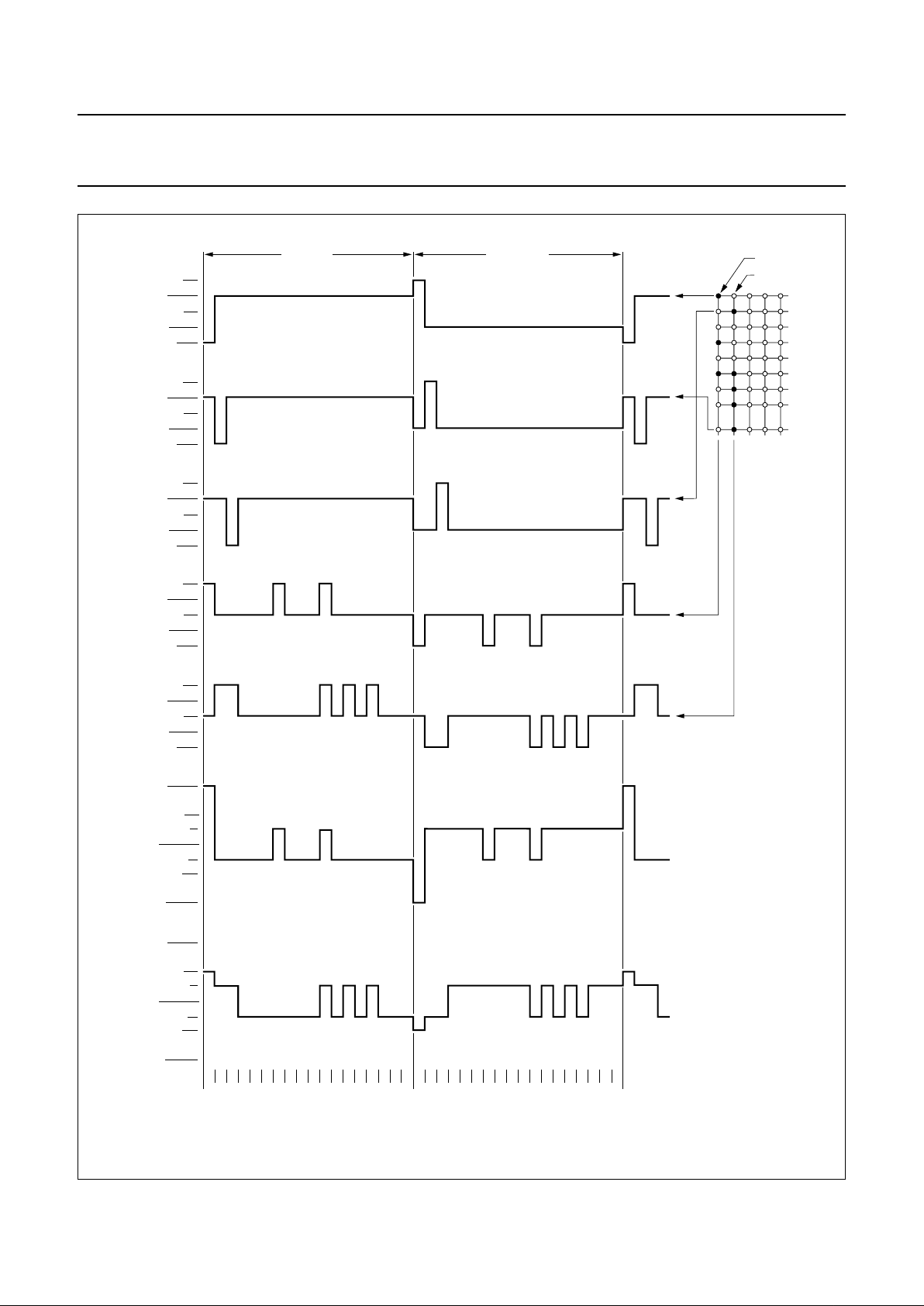
Fig.8 Typical LCD waveforms; character mode.
handbook, full pagewidth
MGE996
state 1 (ON)
state 2 (OFF)
frame n + 1 frame n
123 18123 18
ROW 1
V
LCD
V
2
V3/V
4
V
5
V
SS
ROW 9
V
LCD
V
2
V3/V
4
V
5
V
SS
ROW 2
V
LCD
V
2
V3/V
4
V
5
V
SS
COL1
V
LCD
V
2
V3/V
4
V
5
V
SS
COL2
V
LCD
V
2
V3/V
4
V
5
V
SS
0 V
state 1
V
OP
0.5V
OP
0.25V
OP
−0.25V
OP
−0.5V
OP
−V
OP
0 V
state 2
V
OP
0.5V
OP
0.25V
OP
−0.25V
OP
−0.5V
OP
−V
OP
R1
R2
R3
R4
R5
R6
R7
R8
R9
1998 May 11 14
Philips Semiconductors Product specification
LCD controllers/drivers PCF2103 family
Fig.9 Mux 1 : 2 LCD waveforms; icon mode.
handbook, full pagewidth
MGE997
frame n + 1 frame n
V
LCD
2/3
1/3
V
SS
V
LCD
2/3
1/3
V
SS
V
LCD
2/3
1/3
V
SS
V
LCD
2/3
1/3
V
SS
V
LCD
2/3
1/3
V
SS
V
LCD
2/3
1/3
V
SS
V
LCD
2/3
1/3
V
SS
COL 4
OFF/OFF
COL 3
ON/ON
COL 2
OFF
/ON
COL 1
ON/OFF
ROW 1 to 16
ROW 18
ROW 17
only icons are
driven (MUX 1 : 2)
1998 May 11 15
Philips Semiconductors Product specification
LCD controllers/drivers PCF2103 family
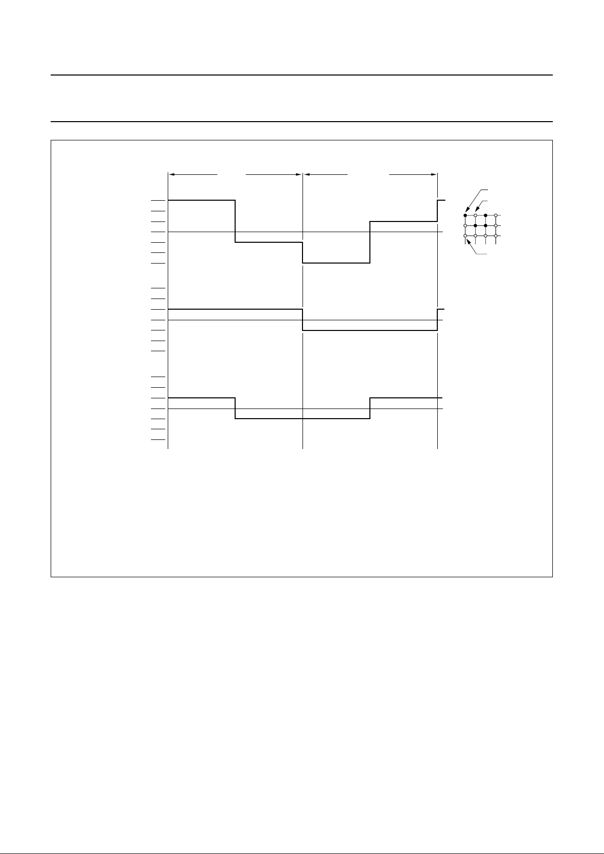
Fig.10 Mux1:2 LCD waveforms; icon mode.
V
ON(rms)
= 0.745 VOP.
V
OFF(rms)
= 0.333 VOP.
D
V
ON
V
OFF
-------------
2.23==
handbook, full pagewidth
MGE998
frame n + 1 frame n
V
OP
2/3 V
OP
1/3 V
OP
0
−1/3 V
OP
−2/3 V
OP
−V
OP
V
OP
2/3 V
OP
1/3 V
OP
0
−1/3 V
OP
−2/3 V
OP
−V
OP
V
OP
2/3 V
OP
1/3 V
OP
0
−1/3 V
OP
−2/3 V
OP
−V
OP
state 3
COL 1 -
ROW 1 to 16
state 2
COL 2 -
ROW 17
state 1
COL 1 -
ROW 17
state 3 (OFF)
R17
R18
R1-16
V
PIXEL
state 1 (ON)
state 2 (OFF)
1998 May 11 16
Philips Semiconductors Product specification
LCD controllers/drivers PCF2103 family
7.15 Reset function
The PCF2103 automatically initializes (resets) when power is turned on. The reset executes a ‘clear display’ instruction,
requiring 165 oscillator cycles. After the reset the chip has the state shown in Table 5.
Table 5 State after reset
STEP INSTRUCTION RESET STATE (BIT/REGISTER) RESET STATE (DESCRIPTION)
1 clear display
2 entry mode set I/D = 1 +1 (increment)
S = 0 no shift
3 display control D = 0 display off
C = 0 cursor off
B = 0 cursor character blink off
4 function set DL = 1 8-bit interface
M = 0 1-line display
H = 0 normal instruction set
5 default address pointer to DDRAM; the Busy Flag (BF) indicates the busy state (BF = 1) until initialization
ends; the busy state lasts 2 ms; the chip may also be initialized by software; see Tables 16 and 17
6 icon control IM, IB = 00 icons/icon blink disabled
7 display/screen configuration L, P, Q = 000 default configurations
8I
2
C-bus interface reset
1998 May 11 17
Philips Semiconductors Product specification
LCD controllers/drivers PCF2103 family
8 INSTRUCTIONS
Only two PCF2103 registers, the Instruction Register (IR)
and the Data Register (DR) can be directly controlled by
the microcontroller. Before internal operation, control
information is stored temporarily in these registers to allow
interface to various types of microcontrollers which
operate at different speeds or to allow interface to
peripheral control ICs. The format for instructions when
I2C-bus control is used is shown in Table 6. The PCF2103
operation is controlled by the instructions given in Table 7
together with their execution time. Details are explained in
subsequent sections.
Instructions are of 4 types, those that:
1. Designate PCF2103 functions such as display format,
data length, etc.
2. Set internal RAM addresses
3. Perform data transfer with internal RAM
4. Others.
In normal use, instructions that perform data transfer with
internal RAM are used most frequently. However,
automatic incrementing by 1 (or decrementing by 1) of
internal RAM addresses after each data write lessens the
microcontroller program load. The display shift in particular
can be performed concurrently with display data write,
enabling the designer to develop systems in minimum time
with maximum programming efficiency.
During internal operation, no instruction other than the
‘read busy flag and address counter’ instruction will be
executed. Because the busy flag is set to logic 1 while an
instruction is being executed, the user should verify that
the busy flag is at logic 0 before sending the next
instruction or wait for the maximum instruction execution
time, as given in Table 7. An instruction sent while the
busy flag is logic 1 will not be executed.
Table 6 Instruction set for I
2
C-bus commands
Note
1. R/
W is set together with the slave address.
CONTROL BYTE COMMAND BYTE I
2
C-BUS COMMANDS
CoRS000000DB7DB6DB5DB4DB3DB2DB1DB0note 1
 Loading...