

Philips PCF2110CU-10-F1, PCF2100CT-F1, PCF2100CU-10-F1, PCF2100CU-F1, PCF2100CP-F1 Datasheet
...
DATA SH EET
Product specification
Supersedes data of 1995 May 03
File under Integrated Circuits, IC12
1997 Mar 28
INTEGRATED CIRCUITS
PCF21xxC family
LCD drivers

1997 Mar 28 2
Philips Semiconductors Product specification
LCD drivers PCF21xxC family
CONTENTS
1 FEATURES
2 GENERAL DESCRIPTION
3 QUICK REFERENCE DATA
4 ORDERING INFORMATION
5 BLOCK DIAGRAMS
6 PINNING
6.1 PCF2100C
6.2 PCF2111C
6.3 PCF2112C
7 FUNCTIONAL DESCRIPTION
7.1 PCF2100C
7.2 PCF2111C
7.3 PCF2112C
7.4 Bus control logic
7.5 Timing
7.6 Input circuitry
7.7 Expansion
8 LIMITING VALUES
9 HANDLING
10 DC CHARACTERISTICS
11 AC CHARACTERISTICS
12 PACKAGE OUTLINES
13 SOLDERING
13.1 Plastic dual in-line packages
13.1.1 By dip or wave
13.1.2 Repairing soldered joints
13.2 Plastic small outline packages
13.2.1 By wave
13.2.2 By solder paste reflow
13.2.3 Repairing soldered joints (by hand-held
soldering iron or pulse-heated solder tool)
14 DEFINITIONS
15 LIFE SUPPORT APPLICATIONS
1997 Mar 28 3
Philips Semiconductors Product specification
LCD drivers PCF21xxC family
1 FEATURES
• Supply voltage 2.25 to 6.0 V
• Low current consumption
• Serial data input
• CBUS control
• One-point built-in oscillator
• Stand-alone or expanded system
• Power-on reset clear
• LCD segments
– 40 (PCF2100C)
– 64 (PCF2111C)
– 32 (PCF2112C)
• Multiplex rate
– 1 : 2 (PCF2100C)
– 1 : 2 (PCF2111C)
– 1 : 1 (PCF2112C)
• Word length
– 22 bits (PCF2100C)
– 34 bits (PCF2111C)
– 34 bits (PCF2112C).
2 GENERAL DESCRIPTION
The PCF21xxC family are single-chip, silicon gate CMOS
LCD driver circuits. A 3-line bus (CBUS) structure enables
serial data transfer with microcontrollers. All inputs are
CMOS/NMOS compatible.
The devices have the same function and performance as
those of the PCF21xx family, which they supersede.
The maximum operating voltage required is reduced from
6.5 to 6.0 V.
3 QUICK REFERENCE DATA
4 ORDERING INFORMATION
SYMBOL PARAMETER CONDITIONS MIN. TYP. MAX. UNIT
V
DD
supply voltage 2.25 − 6.0 V
I
DD1
supply current 1 outputs open; CBUS inactive − 20 50 µA
I
DD2
supply current 2 outputs open; CBUS inactive;
T
amb
=25°C
− 20 30 µA
P
O
power dissipation per output −−100 mW
T
amb
operating ambient temperature −40 − +85 °C
T
stg
storage temperature −65 − +150 °C
TYPE
NUMBER
PACKAGE
NAME DESCRIPTION VERSION
PCF2100CP DIP28 plastic dual in-line package; 28 leads (600 mil) SOT117-1
PCF2100CT SO28 plastic small outline package; 28 leads; body width 7.5 mm SOT136-1
PCF2111CP DIP40 plastic dual in-line package; 40 leads (600 mil) SOT129-1
PCF2111CT VSO40 plastic very small outline package; 40 leads SOT158-1
PCF2112CP DIP40 plastic dual in-line package; 40 leads (600 mil) SOT129-1
PCF2112CT VSO40 plastic very small outline package; 40 leads SOT158-1
1997 Mar 28 4
Philips Semiconductors Product specification
LCD drivers PCF21xxC family
5 BLOCK DIAGRAMS
Fig.1 Block diagram; PCF2100C.
handbook, full pagewidth
BACKPLANE AND SEGMENT DRIVERS
ANALOG
VOLTAGE
BUS
CONTROL
SHIFT
REGISTER
LATCHES
AND
DRIVER CONTROL
OSCILLATOR
AND
DIVIDER
40-SEGMENT LCD
BP2BP1
2526
S1 to S20
24 to 5
2
3
4
DLEN
CLB
DATA
V
SS
V
DD
OSC
680
pF
1 MΩ
R
O
C
O
A
B
28
1
27
MLD286
PCF2100C
Fig.2 Block diagram; PCF2111C.
handbook, full pagewidth
BACKPLANE AND SEGMENT DRIVERS
ANALOG
VOLTAGE
BUS
CONTROL
SHIFT
REGISTER
LATCHES
AND
DRIVER CONTROL
OSCILLATOR
AND
DIVIDER
64-SEGMENT LCD
BP2BP1
3738
2
3
4
DLEN
CLB
DATA
V
SS
V
DD
OSC
680
pF
1 MΩ
R
O
C
O
A
B
40
1
39
MLD285
PCF2111C
S1 to S32
36 to 5

1997 Mar 28 5
Philips Semiconductors Product specification
LCD drivers PCF21xxC family
Fig.3 Block diagram; PCF2112C.
handbook, full pagewidth
BACKPLANE AND SEGMENT DRIVERS
ANALOG
VOLTAGE
BUS
CONTROL
SHIFT
REGISTER
LATCHES
AND
DRIVER CONTROL
OSCILLATOR
AND
DIVIDER
32-SEGMENT LCD
BP
38
2
3
4
DLEN
CLB
DATA
V
SS
V
DD
OSC
1.5
nF
1 MΩ
R
O
C
O
40
1
39
MLD287
PCF2112C
S1 to S32
36 to 5

1997 Mar 28 6
Philips Semiconductors Product specification
LCD drivers PCF21xxC family
6 PINNING
6.1 PCF2100C
SYMBOL PIN DESCRIPTION
CLB 1 clock burst input (CBUS)
V
DD
2 supply voltage
OSC 3 oscillator input
V
SS
4 supply voltage ground
S20 5 LCD driver output 20
S19 6 LCD driver output 19
S18 7 LCD driver output 18
S17 8 LCD driver output 17
S16 9 LCD driver output 16
S15 10 LCD driver output 15
S14 11 LCD driver output 14
S13 12 LCD driver output 13
S12 13 LCD driver output 12
S11 14 LCD driver output 11
S10 15 LCD driver output 10
S9 16 LCD driver output 9
S8 17 LCD driver output 8
S7 18 LCD driver output 7
S6 19 LCD driver output 6
S5 20 LCD driver output 5
S4 21 LCD driver output 4
S3 22 LCD driver output 3
S2 23 LCD driver output 2
S1 24 LCD driver output 1
BP2 25 backplane driver output 2
BP1 26 backplane driver output 1
DATA 27 data input line (CBUS)
DLEN 28 data input line enable (CBUS)
Fig.4 Pin configuration; SOT117-1 and SOT136-1.
handbook, halfpage
PCF2100C
MLD295
1
2
3
4
5
6
7
8
9
10
11
12
13
14
28
27
26
25
24
23
22
21
20
19
18
17
16
15
CLB
V
OSC
S20
S19
S18
S17
S16
S15
S14
S13
S12
S11
DD
V
SS
DLEN
DATA
BP1
BP2
S1
S2
S3
S4
S5
S6
S7
S8
S9
S10
1997 Mar 28 7
Philips Semiconductors Product specification
LCD drivers PCF21xxC family
6.2 PCF2111C
SYMBOL PIN DESCRIPTION
CLB 1 clock burst input (CBUS)
V
DD
2 supply voltage
OSC 3 oscillator input
V
SS
4 supply voltage ground
S32 5 LCD driver output 32
S31 6 LCD driver output 31
S30 7 LCD driver output 30
S29 8 LCD driver output 29
S28 9 LCD driver output 28
S27 10 LCD driver output 27
S26 11 LCD driver output 26
S25 12 LCD driver output 25
S24 13 LCD driver output 24
S23 14 LCD driver output 23
S22 15 LCD driver output 22
S21 16 LCD driver output 21
S20 17 LCD driver output 20
S19 18 LCD driver output 19
S18 19 LCD driver output 18
S17 20 LCD driver output 17
S16 21 LCD driver output 16
S15 22 LCD driver output 15
S14 23 LCD driver output 14
S13 24 LCD driver output 13
S12 25 LCD driver output 12
S11 26 LCD driver output 11
S10 27 LCD driver output 10
S9 28 LCD driver output 9
S8 29 LCD driver output 8
S7 30 LCD driver output 7
S6 31 LCD driver output 6
S5 32 LCD driver output 5
S4 33 LCD driver output 4
S3 34 LCD driver output 3
S2 35 LCD driver output 2
S1 36 LCD driver output 1
BP2 37 backplane driver output 2
BP1 38 backplane driver output 1
DATA 39 data input line (CBUS)
DLEN 40 data input line enable (CBUS)
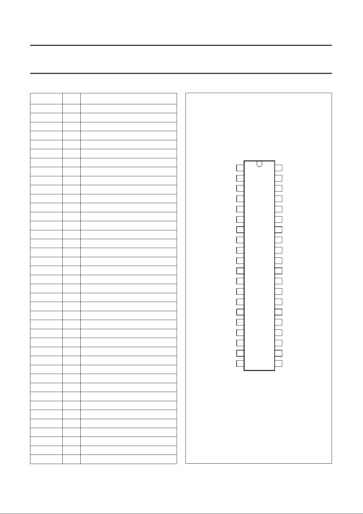
Fig.5 Pin configuration; SOT129-1 and SOT158-1.
handbook, halfpage
PCF2111C
MLD291
1
2
3
4
5
6
7
8
9
10
11
12
13
14
15
16
17
18
19
20
40
39
38
37
36
35
34
33
32
31
30
29
28
27
26
25
24
23
22
21
CLB
V
OSC
S32
S31
S30
S29
S28
S27
S26
S25
S24
S23
S22
S21
S20
S19
S18
S17
DD
V
SS
DLEN
BP1
S1
S2
S3
S4
S5
S6
S7
S8
S9
S10
S11
S12
S13
S14
S15
S16
DATA
BP2
1997 Mar 28 8
Philips Semiconductors Product specification
LCD drivers PCF21xxC family
6.3 PCF2112C
SYMBOL PIN DESCRIPTION
CLB 1 clock burst input (CBUS)
V
DD
2 supply voltage
OSC 3 oscillator input
V
SS
4 supply voltage ground
S32 5 LCD driver output 32
S31 6 LCD driver output 31
S30 7 LCD driver output 30
S29 8 LCD driver output 29
S28 9 LCD driver output 28
S27 10 LCD driver output 27
S26 11 LCD driver output 26
S25 12 LCD driver output 25
S24 13 LCD driver output 24
S23 14 LCD driver output 23
S22 15 LCD driver output 22
S21 16 LCD driver output 21
S20 17 LCD driver output 20
S19 18 LCD driver output 19
S18 19 LCD driver output 18
S17 20 LCD driver output 17
S16 21 LCD driver output 16
S15 22 LCD driver output 15
S14 23 LCD driver output 14
S13 24 LCD driver output 13
S12 25 LCD driver output 12
S11 26 LCD driver output 11
S10 27 LCD driver output 10
S9 28 LCD driver output 9
S8 29 LCD driver output 8
S7 30 LCD driver output 7
S6 31 LCD driver output 6
S5 32 LCD driver output 5
S4 33 LCD driver output 4
S3 34 LCD driver output 3
S2 35 LCD driver output 2
S1 36 LCD driver output 1
n.c. 37 not connected
BP 38 backplane driver output
DATA 39 data input line (CBUS)
DLEN 40 data input line enable (CBUS)
Fig.6 Pin configuration; SOT129-1 and SOT158-1.
handbook, halfpage
PCF2112C
MLD292
1
2
3
4
5
6
7
8
9
10
11
12
13
14
15
16
17
18
19
20
40
39
38
37
36
35
34
33
32
31
30
29
28
27
26
25
24
23
22
21
CLB
V
OSC
S32
S31
S30
S29
S28
S27
S26
S25
S24
S23
S22
S21
S20
S19
S18
S17
DD
V
SS
DLEN
BP
S1
S2
S3
S4
S5
S6
S7
S8
S9
S10
S11
S12
S13
S14
S15
S16
DATA
n.c.

1997 Mar 28 9
Philips Semiconductors Product specification
LCD drivers PCF21xxC family
7 FUNCTIONAL DESCRIPTION
An LCD segment or LED output is activated when the
corresponding DATA bit is HIGH.
7.1 PCF2100C
When DATA bit 21 is HIGH, the A-latches (BP1) are
loaded. With DATA bit 21 LOW, the B-latches (BP2) are
loaded. CLB pulse 23 transfers data from the shift register
to the selected latches.
7.2 PCF2111C
When DATA bit 33 is HIGH, the A-latches (BP1) are
loaded. With DATA bit 33 LOW, the B-latches (BP2) are
loaded. CLB pulse 35 transfers data from the shift register
to the selected latches.
7.3 PCF2112C
When DATA bit 33 is HIGH, the latches are loaded.
CLB pulse 35 transfers data from the shift register to the
selected latches.
7.4 Bus control logic
The following tests are carried out by the bus control logic:
1. Test on leading zero
2. Test on number of DATA bits
3. Test of disturbed DLEN and DATA signals during
transmission.
If one of the test conditions is not fulfilled, no action follows
the load condition (load pulse with DLEN LOW) and the
driver is ready to receive new data.
Fig.7 CBUS data format.
handbook, full pagewidth
DLEN
CLB
DATA
1
01
S1
1
S1
2
S2
2
S2
3
S3
3
S3
4
S4
4
S4
5
S5
5
S5
6
S6
6
S6
7
S7
7
S7
31
S31
19
S19
2345 678 3220332134
22
35
23
PCF2111C and PCF2112C
PCF2100C
PCF2111C and PCF2112C
load bit
load pulse
leading zero
test leading zero
32
S32
20
S20
33
21
PCF2100C
bit number
output
MLD296

1997 Mar 28 10
Philips Semiconductors Product specification
LCD drivers PCF21xxC family
7.5 Timing
Fig.8 Timing diagram for PCF2100C and PCF2111C.
MLD294
V
DD
V
SS
SSDD
0.5 (V V )
SSDD
0.5 (V V )
V
DD
V
SS
SSDD
0.5 (V V )
V
DD
V
SS
SSDD
V V
0
SSDD
0.5 (V V )
SSDD
(V V )
SSDD
0.5 (V V )
SSDD
V V
0
SSDD
0.5 (V V )
SSDD
(V V )
BP2 SX
BP1 SX
BP1
BP2
SX
1
f
LCD
OFF / OFF ON / OFF OFF / ON ON / ON
Fig.9 Timing diagram for PCF2112C.
handbook, halfpage
MLD299
V
DD
V
SS
V
DD
V
SS
SSDD
V V
0
SSDD
(V V )
BP SX
Segment X
(SX)
BP
1
f
LCD
OFF ON

1997 Mar 28 11
Philips Semiconductors Product specification
LCD drivers PCF21xxC family
7.6 Input circuitry
7.7 Expansion
Fig.10 Input circuitry.
VSS line is common. In systems where it is expected that V
DD2>VDD1
+ 0.5V, a resistor should be inserted to reduce the current flowing through the
input protection. Maximum input current ≤40µA.
handbook, halfpage
BUS DRIVER PCF21XXC
R
100 kΩ
V
SS
V
DD2VDD
V
SS
MLD284
Fig.11 Expansion possibility (using PCF2111C).
By connecting OSC to VSS the BP pins become inputs and generate signals synchronized to the single oscillator frequency, thus allowing expansion of
several members of the PCF21xxC family up to the BP drive capability of the master. The PCF2112C can only function as a master for other PCF2112Cs.
handbook, full pagewidth
DLEN
OSC
CLB
DATA
BP2 S1 to S32BP1
V
SS
PCF2111C
SLAVE1
DLEN
OSC
CLB
DATA
BP2 S1 to S32BP1
V
SS
PCF2111C
SLAVE1
DLEN
OSC
CLB
DATA
BP2 S1 to S32BP1
V
SS
V
DD
PCF2111C
MASTER
LCD
MLD293
DATA
CLB
DLEN1
DLEN2
DLEN3

1997 Mar 28 12
Philips Semiconductors Product specification
LCD drivers PCF21xxC family
8 LIMITING VALUES
In accordance with the Absolute Maximum Rating System (IEC 134).
Note
1. Derate by 7.7 mW/K when T
amb
>60°C.
9 HANDLING
Inputs and outputs are protected against electrostatic discharge in normal handling. However, to be totally safe, it is
desirable to take normal precautions appropriate to handling MOS devices. See
“Handling MOS devices”
.
ESD in accordance with
“MIL STD 883C, Method 3015”
.
SYMBOL PARAMETER CONDITIONS MIN. MAX. UNIT
V
DD
supply voltage −0.5 +8.0 V
V
I
input voltage DLEN, CLB, DATA and OSC VSS− 0.5 VDD+ 0.5 V
V
O
output voltage BP1, BP2 and S1 to S32 VSS− 0.5 VDD+ 0.5 V
I
DD
, I
SS
supply current −50 +50 mA
I
I
DC input current −20 +20 mA
I
O
DC output current −25 +25 mA
P
tot
total power dissipation per package note 1 − 500 mW
P
O
power dissipation per output − 100 mW
T
stg
storage temperature −65 +150 °C

1997 Mar 28 13
Philips Semiconductors Product specification
LCD drivers PCF21xxC family
10 DC CHARACTERISTICS
V
DD
= 2.25 to 6.0 V; VSS=0V; T
amb
= −40 to +80 °C; RO=1MΩ; CO= 680 pF; unless otherwise specified.
Notes
1. Outputs open; CBUS inactive.
2. Resets all logic, when V
DD<VPOR
.
3. Periodically sampled (not 100% tested).
4. Outputs measured one at a time.
SYMBOL PARAMETER CONDITIONS MIN. TYP. MAX. UNIT
Supply
V
DD
supply voltage 2.25 − 6.0 V
I
DD
supply current note 1; see Fig.13 − 20 50 µA
note 1; T
amb
=25°C;
see Fig.13
− 20 30 µA
V
POR
power-on reset voltage level note 2 − 1.0 1.6 V
Inputs CLB, DATA and DLEN
V
IL
LOW level input voltage −−0.8 V
V
IH
HIGH level input voltage 2.0 −−V
I
LI
input leakage current VI=VSSor V
DD
−−±1µA
C
i
input capacitance note 3 −−10 pF
Input OSC
I
osc
oscillator start-up current VI=V
SS
0.5 1.2 5.0 µA
LCD outputs
V
BP
DC voltage of backplane drivers −±20 − mV
Z
O(BP)
backplane driver output impedance note 4; VDD=5V − 0.5 5.0 kΩ
Z
O(S)
segment driver output impedance note 4; VDD=5V − 17kΩ

1997 Mar 28 14
Philips Semiconductors Product specification
LCD drivers PCF21xxC family
11 AC CHARACTERISTICS
V
DD
= 2.25 to 6.0 V; VSS=0V; T
amb
= −40 to +80 °C; RO=1MΩ; CO= 680 pF; all timing values are referenced to V
IH
and VIL levels with an input voltage swing of VSSto VDD; unless otherwise specified.
SYMBOL PARAMETER CONDITIONS MIN. TYP. MAX. UNIT
Inputs CLB, DATA and DLEN (see Fig.12)
t
SUDA
data set-up time 3 −−µs
t
HDDA
data hold time 3 −−µs
t
SUEN
enable set-up time 1 −−µs
t
SUDI
disable set-up time 2 −−µs
t
SULD
load pulse set-up time 2.5 −−µs
t
BUSY
busy time 3 −−µs
t
WH
CLB HIGH time 1 −−µs
t
WL
CLB LOW time 5 −−µs
t
CLB
CLB cycle time 10 −−µs
t
r
rise time −−10 µs
t
f
fall time −−10 µs
LCD timing (see Figs. 12, 14, 15, 16 and 17)
f
LCD
LCD frame frequency
PCF2100C, PCF2111C 60 75 100 Hz
PCF2112C C
O
= 1.5 nF 30 35 50 Hz
t
BS
transfer time with test loads VDD=5V − 20 100 µs
t
PLCD
driver delay time with test loads VDD=5V − 20 100 µs

1997 Mar 28 15
Philips Semiconductors Product specification
LCD drivers PCF21xxC family
handbook, full pagewidth
MLD297
BP1, BP2
(except PCF 2112C)
(V = 5 V)
DD
0.5 V
BS
t
CLB
t
SX
V
DD
2
0.5 V
(V = 5 V)
DD
0.5 V
0.5 V
0.5 V
0.5 V
(V = 5 V)
DD
enable disable
V
IL max
V
IL max
V
IL max
V
IL max
V
IH min
V
IH min
V
IH min
V
IH min
V
IH min
V
IL max
DLEN
t
r
t
r
t
f
t
f
t
HDDA
t
SUDA
t
SUEN
t
SUDA
t
SUDI
t
SULD
t
BUSY
t
PCLD
t
HDDA
t
WH
t
WL
t
WL
leading zero data S1 load bit
load pulse
12
22
34
23 (1)
35 (2)
BP (PCF2112C)
CLB
DATA
Fig.12 CBUS timing.
(1) Load pulse 23 for PCF2100C (see Fig.7).
(2) Load pulse 35 for PCF2111C and PCF2112C (see Fig.7).

1997 Mar 28 16
Philips Semiconductors Product specification
LCD drivers PCF21xxC family
Fig.13 Supply current as a function of supply
voltage.
(1) T
amb
= −40°c.
(2) T
amb
= +85°c.
(3) T
amb
= +25°c.
handbook, halfpage
024 8
20
8
12
16
MLD283
6
I
DD
(µA)
(1)
(2)
(3)
typ
DD
V (V)
Fig.14 Display frequency as a function of supply
voltage; CO= 680 pF (except PCF2112C).
(1) T
amb
= −40°c.
(2) T
amb
= +25°c.
(3) T
amb
= +85°c.
handbook, halfpage
024 8
80
70
78
MLD282
6
76
74
72
V (V)
DD
f
LCD
(Hz)
typ
(1)
(2)
(3)
Fig.15 Display frequency as a function of supply
voltage; CO= 1.5 nF (only PCF2112C).
(1) T
amb
= −40°c.
(2) T
amb
= +25°c.
(3) T
amb
= +85°c.
handbook, halfpage
024 8
37
36
34
33
35
MLD289
6
f
LCD
(Hz)
typ
(1)
(2)
(3)
DD
V (V)
Fig.16 Display frequency as a function of RO and
CO; T
amb
=25°C; VDD=5V.
(1) RO=1MΩ.
(2) RO= 100kΩ.
handbook, halfpage
10
MLD281
110
1
10
10
3
10
2
C (nF)
O
f
LCD
(Hz)
typ
(1)
(2)

1997 Mar 28 17
Philips Semiconductors Product specification
LCD drivers PCF21xxC family
Fig.17 Test loads.
handbook, halfpage
MLD298
S1 to S32
BP (PCF2112C), BP1, BP2
I = 15 µA
L
I = 25 µA
L
Fig.18 Output resistance of backplane and
segments.
(1) T
amb
= +85°c.
(2) T
amb
= +25°c.
(3) T
amb
= −40°c.
handbook, halfpage
024 8
2
1.5
0.5
0
1
MLD288
6
R
O
(kΩ)
DD
V (V)
typ
(1)
(2)
(3)
(1)
(2)
(3)
R
S
R
BP
Fig.19 LOW level output current as a function of
supply voltage (only PCF2112C).
(1) T
amb
= −40°c.
(2) T
amb
= +25°c.
(3) T
amb
= +85°c.
handbook, halfpage
024 8
18
8
16
MLD290
6
14
12
10
V (V)
DD
I
OL
(mA)
typ
(1)
(2)
(3)

1997 Mar 28 18
Philips Semiconductors Product specification
LCD drivers PCF21xxC family
12 PACKAGE OUTLINES
UNIT
A
max.
1 2
b
1
(1)
(1) (1)
cD E weM
H
L
REFERENCES
OUTLINE
VERSION
EUROPEAN
PROJECTION
ISSUE DATE
IEC JEDEC EIAJ
mm
inches
DIMENSIONS (inch dimensions are derived from the original mm dimensions)
SOT117-1
92-11-17
95-01-14
A
min.
A
max.
b
Z
max.
M
E
e
1
1.7
1.3
0.53
0.38
0.32
0.23
36.0
35.0
14.1
13.7
3.9
3.4
0.252.54 15.24
15.80
15.24
17.15
15.90
1.75.1 0.51 4.0
0.066
0.051
0.020
0.014
0.013
0.009
1.41
1.34
0.56
0.54
0.15
0.13
0.010.10 0.60
0.62
0.60
0.68
0.63
0.0670.20 0.020 0.16
051G05 MO-015AH
M
H
c
(e )
1
M
E
A
L
seating plane
A
1
w M
b
1
e
D
A
2
Z
28
1
15
14
b
E
pin 1 index
0 5 10 mm
scale
Note
1. Plastic or metal protrusions of 0.25 mm maximum per side are not included.
handbook, full pagewidth
DIP28: plastic dual in-line package; 28 leads (600 mil)
SOT117-1

1997 Mar 28 19
Philips Semiconductors Product specification
LCD drivers PCF21xxC family
UNIT
A
max.
1 2
b
1
cD E e M
H
L
REFERENCES
OUTLINE
VERSION
EUROPEAN
PROJECTION
ISSUE DATE
IEC JEDEC EIAJ
mm
inches
DIMENSIONS (inch dimensions are derived from the original mm dimensions)
SOT129-1
92-11-17
95-01-14
A
min.
A
max.
b
Z
max.
w
M
E
e
1
1.70
1.14
0.53
0.38
0.36
0.23
52.50
51.50
14.1
13.7
3.60
3.05
0.2542.54 15.24
15.80
15.24
17.42
15.90
2.254.7 0.51 4.0
0.067
0.045
0.021
0.015
0.014
0.009
2.067
2.028
0.56
0.54
0.14
0.12
0.010.10 0.60
0.62
0.60
0.69
0.63
0.089 0.19 0.020 0.16
051G08 MO-015AJ
M
H
c
(e )
1
M
E
A
L
seating plane
A
1
w M
b
1
e
D
A
2
Z
40
1
21
20
b
E
pin 1 index
0 5 10 mm
scale
Note
1. Plastic or metal protrusions of 0.25 mm maximum per side are not included.
(1)
(1)(1)
DIP40: plastic dual in-line package; 40 leads (600 mil)
SOT129-1

1997 Mar 28 20
Philips Semiconductors Product specification
LCD drivers PCF21xxC family
UNIT
A
max.
A
1
A
2
A3b
p
cD
(1)E(1) (1)
eHELLpQ
Z
ywv θ
REFERENCES
OUTLINE
VERSION
EUROPEAN
PROJECTION
ISSUE DATE
IEC JEDEC EIAJ
mm
inches
2.65
0.30
0.10
2.45
2.25
0.49
0.36
0.32
0.23
18.1
17.7
7.6
7.4
1.27
10.65
10.00
1.1
1.0
0.9
0.4
8
0
o
o
0.25 0.1
DIMENSIONS (inch dimensions are derived from the original mm dimensions)
Note
1. Plastic or metal protrusions of 0.15 mm maximum per side are not included.
1.1
0.4
SOT136-1
91-08-13
95-01-24
X
14
28
w M
θ
A
A
1
A
2
b
p
D
H
E
L
p
Q
detail X
E
Z
c
L
v M
A
e
15
1
(A )
3
A
y
0.25
075E06 MS-013AE
pin 1 index
0.10
0.012
0.004
0.096
0.089
0.019
0.014
0.013
0.009
0.71
0.69
0.30
0.29
0.050
1.4
0.055
0.42
0.39
0.043
0.039
0.035
0.016
0.01
0.25
0.01
0.004
0.043
0.016
0.01
0 5 10 mm
scale
SO28: plastic small outline package; 28 leads; body width 7.5 mm
SOT136-1

1997 Mar 28 21
Philips Semiconductors Product specification
LCD drivers PCF21xxC family
UNIT A1A
2
A3b
p
cD
(1)E(2)
Z
(1)
eHELLpQywv θ
REFERENCES
OUTLINE
VERSION
EUROPEAN
PROJECTION
ISSUE DATE
IEC JEDEC EIAJ
mm
inches
0.3
0.1
2.45
2.25
0.25
0.42
0.30
0.22
0.14
15.6
15.2
7.6
7.5
0.762 2.25
12.3
11.8
1.15
1.05
0.6
0.3
7
0
o
o
0.1 0.1
DIMENSIONS (inch dimensions are derived from the original mm dimensions)
Notes
1. Plastic or metal protrusions of 0.4 mm maximum per side are not included.
2. Plastic interlead protrusions of 0.25 mm maximum per side are not included.
1.7
1.5
SOT158-1
92-11-17
95-01-24
X
w M
θ
A
A
1
A
2
b
p
D
H
E
L
p
Q
detail X
E
Z
e
c
L
v M
A
(A )
3
A
y
40
20
21
1
pin 1 index
0.012
0.004
0.096
0.089
0.017
0.012
0.0087
0.0055
0.61
0.60
0.30
0.29
0.03 0.089
0.48
0.46
0.045
0.041
0.024
0.012
0.004
0.2
0.008 0.004
0.067
0.059
0.010
0 5 10 mm
scale
VSO40: plastic very small outline package; 40 leads
SOT158-1
A
max.
2.70
0.11

1997 Mar 28 22
Philips Semiconductors Product specification
LCD drivers PCF21xxC family
13 SOLDERING
13.1 Introduction
There is no soldering method that is ideal for all IC
packages. Wave soldering is often preferred when
through-hole and surface mounted components are mixed
on one printed-circuit board. However, wave soldering is
not always suitable for surface mounted ICs, or for
printed-circuits with high population densities. In these
situations reflow soldering is often used.
This text gives a very brief insight to a complex technology.
A more in-depth account of soldering ICs can be found in
our
“IC Package Databook”
(order code 9398 652 90011).
13.2 DIP
13.2.1 S
OLDERING BY DIPPING OR BY WA VE
The maximum permissible temperature of the solder is
260 °C; solder at this temperature must not be in contact
with the joint for more than 5 seconds. The total contact
time of successive solder waves must not exceed
5 seconds.
The device may be mounted up to the seating plane, but
the temperature of the plastic body must not exceed the
specified maximum storage temperature (T
stg max
). If the
printed-circuit board has been pre-heated, forced cooling
may be necessary immediately after soldering to keep the
temperature within the permissible limit.
13.2.2 R
EPAIRING SOLDERED JOINTS
Apply a low voltage soldering iron (less than 24 V) to the
lead(s) of the package, below the seating plane or not
more than 2 mm above it. If the temperature of the
soldering iron bit is less than 300 °C it may remain in
contact for up to 10 seconds. If the bit temperature is
between 300 and 400 °C, contact may be up to 5 seconds.
13.3 SO and VSO
13.3.1 REFLOW SOLDERING
Reflow soldering techniques are suitable for all SO and
VSO packages.
Reflow soldering requires solder paste (a suspension of
fine solder particles, flux and binding agent) to be applied
to the printed-circuit board by screen printing, stencilling or
pressure-syringe dispensing before package placement.
Several techniques exist for reflowing; for example,
thermal conduction by heated belt. Dwell times vary
between 50 and 300 seconds depending on heating
method. Typical reflow temperatures range from
215 to 250 °C.
Preheating is necessary to dry the paste and evaporate
the binding agent. Preheating duration: 45 minutes at
45 °C.
13.3.2 W
AVE SOLDERING
Wave soldering techniques can be used for all SO and
VSO packages if the following conditions are observed:
• A double-wave (a turbulent wave with high upward
pressure followed by a smooth laminar wave) soldering
technique should be used.
• The longitudinal axis of the package footprint must be
parallel to the solder flow.
• The package footprint must incorporate solder thieves at
the downstream end.
During placement and before soldering, the package must
be fixed with a droplet of adhesive. The adhesive can be
applied by screen printing, pin transfer or syringe
dispensing. The package can be soldered after the
adhesive is cured.
Maximum permissible solder temperature is 260 °C, and
maximum duration of package immersion in solder is
10 seconds, if cooled to less than 150 °C within
6 seconds. Typical dwell time is 4 seconds at 250 °C.
A mildly-activated flux will eliminate the need for removal
of corrosive residues in most applications.
13.3.3 R
EPAIRING SOLDERED JOINTS
Fix the component by first soldering two diagonallyopposite end leads. Use only a low voltage soldering iron
(less than 24 V) applied to the flat part of the lead. Contact
time must be limited to 10 seconds at up to 300 °C. When
using a dedicated tool, all other leads can be soldered in
one operation within 2 to 5 seconds between
270 and 320 °C.

1997 Mar 28 23
Philips Semiconductors Product specification
LCD drivers PCF21xxC family
14 DEFINITIONS
15 LIFE SUPPORT APPLICATIONS
These products are not designed for use in life support appliances, devices, or systems where malfunction of these
products can reasonably be expected to result in personal injury. Philips customers using or selling these products for
use in such applications do so at their own risk and agree to fully indemnify Philips for any damages resulting from such
improper use or sale.
Data sheet status
Objective specification This data sheet contains target or goal specifications for product development.
Preliminary specification This data sheet contains preliminary data; supplementary data may be published later.
Product specification This data sheet contains final product specifications.
Short-form specification The data in this specification is extracted from a full data sheet with the same type
number and title. For detailed information see the relevant data sheet or data handbook.
Limiting values
Limiting values given are in accordance with the Absolute Maximum Rating System (IEC 134). Stress above one or
more of the limiting values may cause permanent damage to the device. These are stress ratings only and operation
of the device at these or at any other conditions above those given in the Characteristics sections of the specification
is not implied. Exposure to limiting values for extended periods may affect device reliability.
Application information
Where application information is given, it is advisory and does not form part of the specification.

Internet: http://www.semiconductors.philips.com
Philips Semiconductors – a worldwide company
© Philips Electronics N.V. 1997 SCA53
All rights are reserved. Reproduction in whole or in part is prohibited without the prior written consent of the copyright owner.
The information presented in this document does not form part of any quotation or contract, is believed to be accurate and reliable and may be changed
without notice. No liability will be accepted by the publisher for any consequence of its use. Publication thereof does not convey nor imply any license
under patent- or other industrial or intellectual property rights.
Netherlands: Postbus 90050, 5600 PB EINDHOVEN, Bldg. VB,
Tel. +31 40 27 82785, Fax. +31 40 27 88399
New Zealand: 2 Wagener Place, C.P.O. Box 1041, AUCKLAND,
Tel. +64 9 849 4160, Fax. +64 9 849 7811
Norway: Box 1, Manglerud 0612, OSLO,
Tel. +47 22 74 8000, Fax. +47 22 74 8341
Philippines: Philips Semiconductors Philippines Inc.,
106 Valero St. Salcedo Village, P.O. Box 2108 MCC, MAKATI,
Metro MANILA, Tel. +63 2 816 6380, Fax. +63 2 817 3474
Poland: Ul. Lukiska 10, PL 04-123 WARSZAWA,
Tel. +48 22 612 2831, Fax. +48 22 612 2327
Portugal: see Spain
Romania: see Italy
Russia: Philips Russia, Ul. Usatcheva 35A, 119048 MOSCOW,
Tel. +7 095 755 6918, Fax. +7 095 755 6919
Singapore: Lorong 1, Toa Payoh, SINGAPORE 1231,
Tel. +65 350 2538, Fax. +65 251 6500
Slovakia: see Austria
Slovenia: see Italy
South Africa: S.A. PHILIPS Pty Ltd., 195-215 Main Road Martindale,
2092 JOHANNESBURG, P.O. Box 7430 Johannesburg 2000,
Tel. +27 11 470 5911, Fax. +27 11 470 5494
South America: Rua do Rocio 220, 5th floor, Suite 51,
04552-903 São Paulo, SÃO PAULO - SP, Brazil,
Tel. +55 11 821 2333, Fax. +55 11 829 1849
Spain: Balmes 22, 08007 BARCELONA,
Tel. +34 3 301 6312, Fax. +34 3 301 4107
Sweden: Kottbygatan 7, Akalla, S-16485 STOCKHOLM,
Tel. +46 8 632 2000, Fax. +46 8 632 2745
Switzerland: Allmendstrasse 140, CH-8027 ZÜRICH,
Tel. +41 1 488 2686, Fax. +41 1 481 7730
Taiwan: Philips Semiconductors, 6F, No. 96, Chien Kuo N. Rd., Sec. 1,
TAIPEI, Taiwan Tel. +886 2 2134 2870, Fax. +886 2 2134 2874
Thailand: PHILIPS ELECTRONICS (THAILAND) Ltd.,
209/2 Sanpavuth-Bangna Road Prakanong, BANGKOK 10260,
Tel. +66 2 745 4090, Fax. +66 2 398 0793
Turkey: Talatpasa Cad. No. 5, 80640 GÜLTEPE/ISTANBUL,
Tel. +90 212 279 2770, Fax. +90 212 282 6707
Ukraine: PHILIPS UKRAINE, 4 Patrice Lumumba str., Building B, Floor 7,
252042 KIEV, Tel. +380 44 264 2776, Fax. +380 44 268 0461
United Kingdom: Philips Semiconductors Ltd., 276 Bath Road, Hayes,
MIDDLESEX UB3 5BX, Tel. +44 181 730 5000, Fax. +44 181 754 8421
United States: 811 East Arques Avenue, SUNNYVALE, CA 94088-3409,
Tel. +1 800 234 7381
Uruguay: see South America
Vietnam: see Singapore
Yugoslavia: PHILIPS, Trg N. Pasica 5/v, 11000 BEOGRAD,
Tel. +381 11 625 344, Fax.+381 11 635 777
For all other countries apply to: Philips Semiconductors, Marketing & Sales Communications,
Building BE-p, P.O. Box 218, 5600 MD EINDHOVEN, The Netherlands, Fax. +31 40 27 24825
Argentina: see South America
Australia: 34 Waterloo Road, NORTH RYDE, NSW 2113,
Tel. +61 2 9805 4455, Fax. +61 2 9805 4466
Austria: Computerstr. 6, A-1101 WIEN, P.O. Box 213,
Tel. +43 1 60 101, Fax. +43 1 60 101 1210
Belarus: Hotel Minsk Business Center, Bld. 3, r. 1211, Volodarski Str. 6,
220050 MINSK, Tel. +375 172 200 733, Fax. +375 172 200 773
Belgium: see The Netherlands
Brazil: seeSouth America
Bulgaria: Philips Bulgaria Ltd., Energoproject, 15thfloor,
51 James Bourchier Blvd., 1407 SOFIA,
Tel. +359 2 689 211, Fax. +359 2 689 102
Canada: PHILIPS SEMICONDUCTORS/COMPONENTS,
Tel. +1 800 234 7381
China/Hong Kong: 501 Hong Kong Industrial Technology Centre,
72 Tat Chee Avenue, Kowloon Tong, HONG KONG,
Tel. +852 2319 7888, Fax. +852 2319 7700
Colombia: see South America
Czech Republic: see Austria
Denmark: Prags Boulevard 80, PB 1919, DK-2300 COPENHAGEN S,
Tel. +45 32 88 2636, Fax. +45 31 57 1949
Finland: Sinikalliontie 3, FIN-02630 ESPOO,
Tel. +358 9 615800, Fax. +358 9 61580/xxx
France: 4 Rue du Port-aux-Vins, BP317, 92156 SURESNES Cedex,
Tel. +33 1 40 99 6161, Fax. +33 1 40 99 6427
Germany: Hammerbrookstraße 69, D-20097 HAMBURG,
Tel. +49 40 23 53 60, Fax. +49 40 23 536 300
Greece: No. 15, 25th March Street, GR 17778 TAVROS/ATHENS,
Tel. +30 1 4894 339/239, Fax. +30 1 4814 240
Hungary: seeAustria
India: Philips INDIA Ltd, Shivsagar Estate, A Block, Dr. Annie Besant Rd.
Worli, MUMBAI 400 018, Tel. +91 22 4938 541, Fax. +91 22 4938 722
Indonesia: see Singapore
Ireland: Newstead, Clonskeagh, DUBLIN 14,
Tel. +353 1 7640 000, Fax. +353 1 7640 200
Israel: RAPAC Electronics, 7 Kehilat Saloniki St, TEL AVIV 61180,
Tel. +972 3 645 0444, Fax. +972 3 649 1007
Italy: PHILIPS SEMICONDUCTORS, Piazza IV Novembre 3,
20124 MILANO, Tel. +39 2 6752 2531, Fax. +39 2 6752 2557
Japan: Philips Bldg 13-37, Kohnan 2-chome, Minato-ku, TOKYO 108,
Tel. +81 3 3740 5130, Fax. +81 3 3740 5077
Korea: Philips House, 260-199 Itaewon-dong, Yongsan-ku, SEOUL,
Tel. +82 2 709 1412, Fax. +82 2 709 1415
Malaysia: No. 76 Jalan Universiti, 46200 PETALING JAYA, SELANGOR,
Tel. +60 3 750 5214, Fax. +60 3 757 4880
Mexico: 5900 Gateway East, Suite 200, EL PASO, TEXAS 79905,
Tel. +9-5 800 234 7381
Middle East: see Italy
Printed in The Netherlands 417067/1200/02/pp24 Date of release: 1997 Mar 28 Document order number: 9397 750 01649
 Loading...