

Philips PCF2111CP, PCF2100CT, PCF2100CP, PCF2112CP Datasheet
INTEGRATED CIRCUITS
DATA SH EET
PCF21xxC family
LCD drivers
Product specification
Supersedes data of 1995 May 03
File under Integrated Circuits, IC12
1997 Mar 28

Philips Semiconductors Product specification
LCD drivers PCF21xxC family
CONTENTS
1 FEATURES
2 GENERAL DESCRIPTION
3 QUICK REFERENCE DATA
4 ORDERING INFORMATION
5 BLOCK DIAGRAMS
6 PINNING
6.1 PCF2100C
6.2 PCF2111C
6.3 PCF2112C
7 FUNCTIONAL DESCRIPTION
7.1 PCF2100C
7.2 PCF2111C
7.3 PCF2112C
7.4 Bus control logic
7.5 Timing
7.6 Input circuitry
7.7 Expansion
8 LIMITING VALUES
9 HANDLING
10 DC CHARACTERISTICS
11 AC CHARACTERISTICS
12 PACKAGE OUTLINES
13 SOLDERING
13.1 Plastic dual in-line packages
13.1.1 By dip or wave
13.1.2 Repairing soldered joints
13.2 Plastic small outline packages
13.2.1 By wave
13.2.2 By solder paste reflow
13.2.3 Repairing soldered joints (by hand-held
soldering iron or pulse-heated solder tool)
14 DEFINITIONS
15 LIFE SUPPORT APPLICATIONS
1997 Mar 28 2
Philips Semiconductors Product specification
LCD drivers PCF21xxC family
1 FEATURES
• Supply voltage 2.25 to 6.0 V
• Low current consumption
• Serial data input
• CBUS control
• One-point built-in oscillator
• Stand-alone or expanded system
• Power-on reset clear
• LCD segments
– 40 (PCF2100C)
– 64 (PCF2111C)
– 32 (PCF2112C)
• Multiplex rate
– 1 : 2 (PCF2100C)
– 1 : 2 (PCF2111C)
– 1 : 1 (PCF2112C)
• Word length
– 22 bits (PCF2100C)
– 34 bits (PCF2111C)
– 34 bits (PCF2112C).
2 GENERAL DESCRIPTION
The PCF21xxC family are single-chip, silicon gate CMOS
LCD driver circuits. A 3-line bus (CBUS) structure enables
serial data transfer with microcontrollers. All inputs are
CMOS/NMOS compatible.
The devices have the same function and performance as
those of the PCF21xx family, which they supersede.
The maximum operating voltage required is reduced from
6.5 to 6.0 V.
3 QUICK REFERENCE DATA
SYMBOL PARAMETER CONDITIONS MIN. TYP. MAX. UNIT
V
I
DD1
I
DD2
P
T
T
DD
O
amb
stg
supply voltage 2.25 − 6.0 V
supply current 1 outputs open; CBUS inactive − 20 50 µA
supply current 2 outputs open; CBUS inactive;
T
=25°C
amb
− 20 30 µA
power dissipation per output −−100 mW
operating ambient temperature −40 − +85 °C
storage temperature −65 − +150 °C
4 ORDERING INFORMATION
TYPE
NUMBER
NAME DESCRIPTION VERSION
PACKAGE
PCF2100CP DIP28 plastic dual in-line package; 28 leads (600 mil) SOT117-1
PCF2100CT SO28 plastic small outline package; 28 leads; body width 7.5 mm SOT136-1
PCF2111CP DIP40 plastic dual in-line package; 40 leads (600 mil) SOT129-1
PCF2111CT VSO40 plastic very small outline package; 40 leads SOT158-1
PCF2112CP DIP40 plastic dual in-line package; 40 leads (600 mil) SOT129-1
PCF2112CT VSO40 plastic very small outline package; 40 leads SOT158-1
1997 Mar 28 3
Philips Semiconductors Product specification
LCD drivers PCF21xxC family
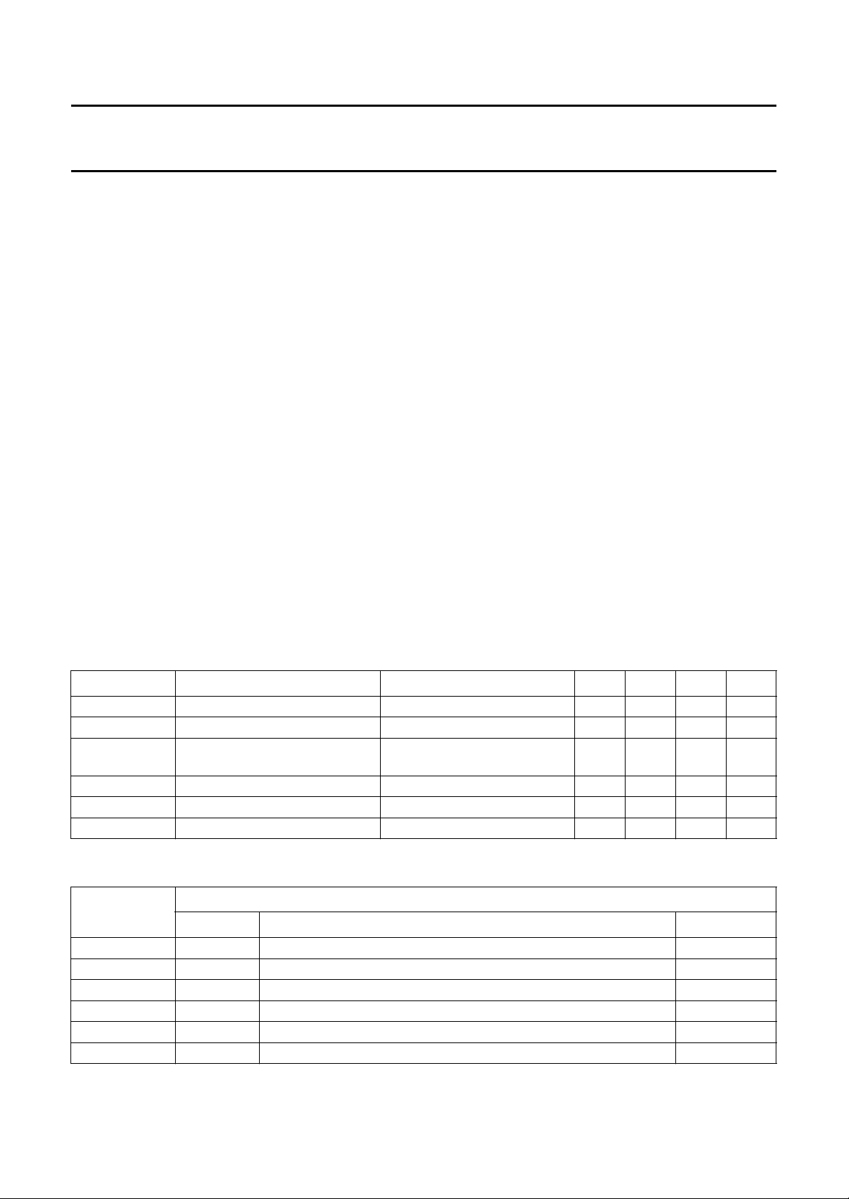
5 BLOCK DIAGRAMS
handbook, full pagewidth
DLEN
CLB
DATA
40-SEGMENT LCD
BP2BP1
2526
BACKPLANE AND SEGMENT DRIVERS
28
1
27
BUS
CONTROL
A
B
DRIVER CONTROL
LATCHES
REGISTER
Fig.1 Block diagram; PCF2100C.
AND
SHIFT
S1 to S20
24 to 5
ANALOG
VOLTAGE
OSCILLATOR
AND
DIVIDER
PCF2100C
2
3
4
MLD286
V
DD
C
OSC
R
V
SS
680
O
pF
1 MΩ
O
handbook, full pagewidth
DLEN
CLB
DATA
BP2BP1
3738
BACKPLANE AND SEGMENT DRIVERS
40
1
BUS
CONTROL
39
64-SEGMENT LCD
A
B
DRIVER CONTROL
LATCHES
AND
SHIFT
REGISTER
Fig.2 Block diagram; PCF2111C.
1997 Mar 28 4
S1 to S32
36 to 5
ANALOG
VOLTAGE
OSCILLATOR
AND
DIVIDER
PCF2111C
2
3
4
MLD285
V
DD
C
OSC
R
V
SS
680
O
pF
1 MΩ
O
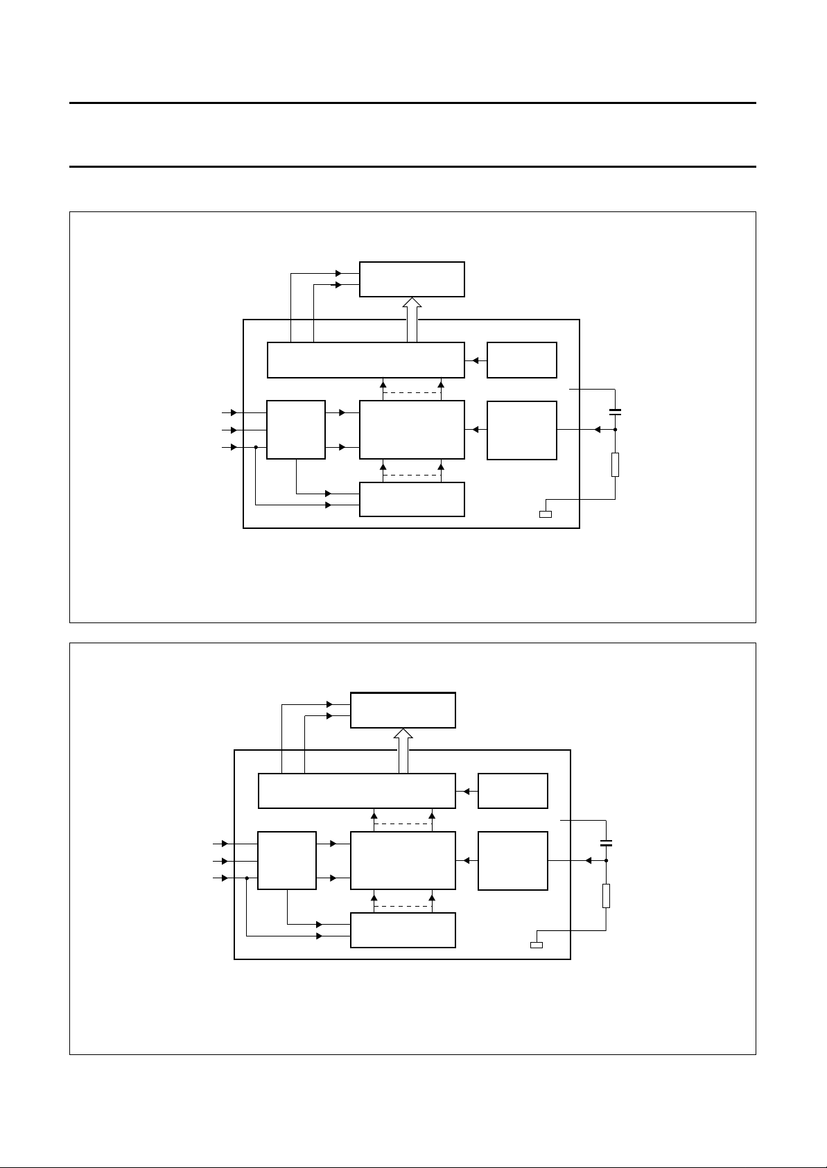
Philips Semiconductors Product specification
LCD drivers PCF21xxC family
handbook, full pagewidth
DLEN
CLB
DATA
32-SEGMENT LCD
BP
38
BACKPLANE AND SEGMENT DRIVERS
40
1
39
BUS
CONTROL
LATCHES
DRIVER CONTROL
REGISTER
Fig.3 Block diagram; PCF2112C.
AND
SHIFT
S1 to S32
36 to 5
ANALOG
VOLTAGE
OSCILLATOR
AND
DIVIDER
PCF2112C
MLD287
V
DD
2
1.5
C
O
OSC
R
V
SS
nF
1 MΩ
O
3
4
1997 Mar 28 5
Philips Semiconductors Product specification
LCD drivers PCF21xxC family
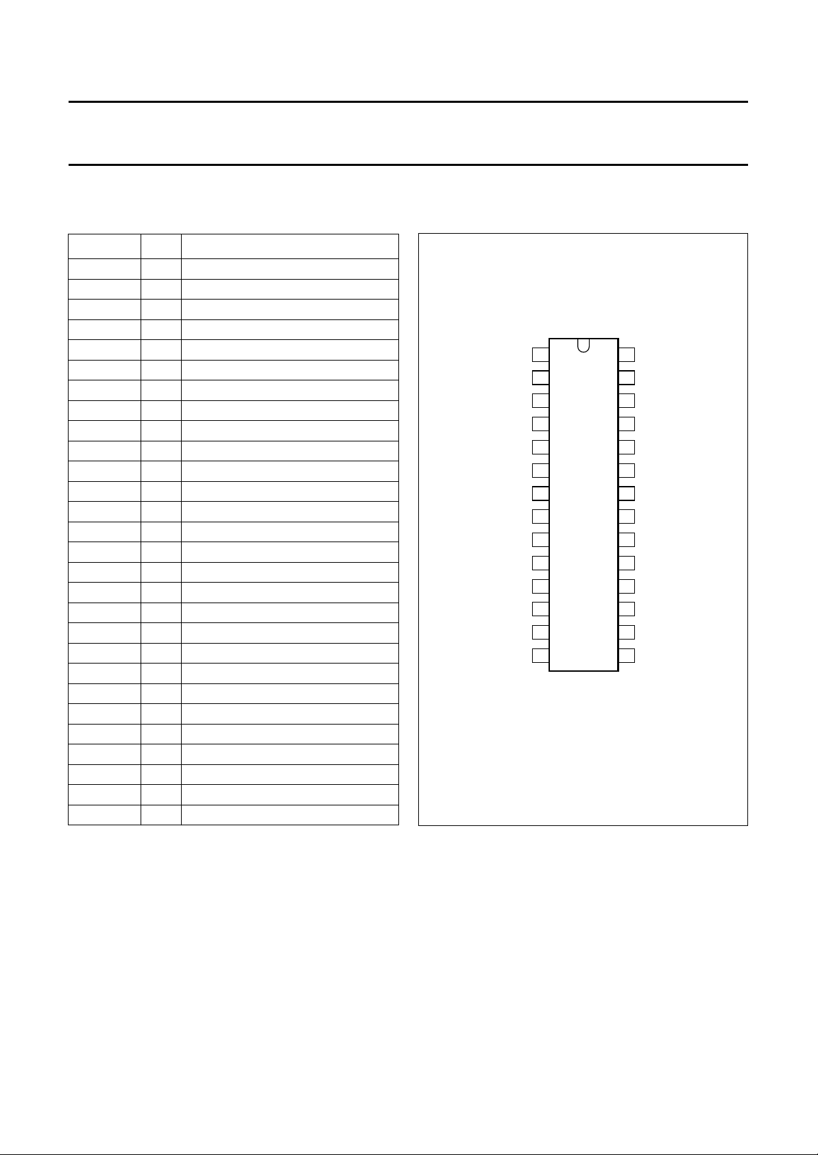
6 PINNING
6.1 PCF2100C
SYMBOL PIN DESCRIPTION
CLB 1 clock burst input (CBUS)
V
DD
OSC 3 oscillator input
V
SS
S20 5 LCD driver output 20
S19 6 LCD driver output 19
S18 7 LCD driver output 18
S17 8 LCD driver output 17
S16 9 LCD driver output 16
S15 10 LCD driver output 15
S14 11 LCD driver output 14
S13 12 LCD driver output 13
S12 13 LCD driver output 12
S11 14 LCD driver output 11
S10 15 LCD driver output 10
S9 16 LCD driver output 9
S8 17 LCD driver output 8
S7 18 LCD driver output 7
S6 19 LCD driver output 6
S5 20 LCD driver output 5
S4 21 LCD driver output 4
S3 22 LCD driver output 3
S2 23 LCD driver output 2
S1 24 LCD driver output 1
BP2 25 backplane driver output 2
BP1 26 backplane driver output 1
DATA 27 data input line (CBUS)
DLEN 28 data input line enable (CBUS)
2 supply voltage
4 supply voltage ground
handbook, halfpage
CLB
V
DD
OSC
V
SS
S20
S19
S18
1
2
3
4
5
6
7
DLEN
28
27
DATA
26
BP1
25
BP2
S1
24
23
S2
22
S3
PCF2100C
S17
S16
S15
S14
S13
S12
S11
8
9
10
11
12
13
14
MLD295
21
S4
20
S5
19
S6
18
S7
S8
17
S9
16
15
S10
Fig.4 Pin configuration; SOT117-1 and SOT136-1.
1997 Mar 28 6

Philips Semiconductors Product specification
LCD drivers PCF21xxC family
6.2 PCF2111C
SYMBOL PIN DESCRIPTION
CLB 1 clock burst input (CBUS)
V
DD
OSC 3 oscillator input
V
SS
S32 5 LCD driver output 32
S31 6 LCD driver output 31
S30 7 LCD driver output 30
S29 8 LCD driver output 29
S28 9 LCD driver output 28
S27 10 LCD driver output 27
S26 11 LCD driver output 26
S25 12 LCD driver output 25
S24 13 LCD driver output 24
S23 14 LCD driver output 23
S22 15 LCD driver output 22
S21 16 LCD driver output 21
S20 17 LCD driver output 20
S19 18 LCD driver output 19
S18 19 LCD driver output 18
S17 20 LCD driver output 17
S16 21 LCD driver output 16
S15 22 LCD driver output 15
S14 23 LCD driver output 14
S13 24 LCD driver output 13
S12 25 LCD driver output 12
S11 26 LCD driver output 11
S10 27 LCD driver output 10
S9 28 LCD driver output 9
S8 29 LCD driver output 8
S7 30 LCD driver output 7
S6 31 LCD driver output 6
S5 32 LCD driver output 5
S4 33 LCD driver output 4
S3 34 LCD driver output 3
S2 35 LCD driver output 2
S1 36 LCD driver output 1
BP2 37 backplane driver output 2
BP1 38 backplane driver output 1
DATA 39 data input line (CBUS)
DLEN 40 data input line enable (CBUS)
2 supply voltage
4 supply voltage ground
handbook, halfpage
CLB
V
DD
OSC
V
SS
S32
S31
S30
S29
S28
S27
S26
S25
S24
S23
S22
S21
S20
S19
S18
S17
1
2
3
4
5
6
7
8
9
10
PCF2111C
11
12
13
14
15
16
17
18
19
20
MLD291
40
DLEN
39
DATA
38
BP1
37
BP2
S1
36
S2
35
34
S3
33
S4
32
S5
31
S6
30
S7
S8
29
S9
28
S10
27
26
S11
25
S12
S13
24
S14
23
S15
22
21
S16
Fig.5 Pin configuration; SOT129-1 and SOT158-1.
1997 Mar 28 7
Philips Semiconductors Product specification
LCD drivers PCF21xxC family
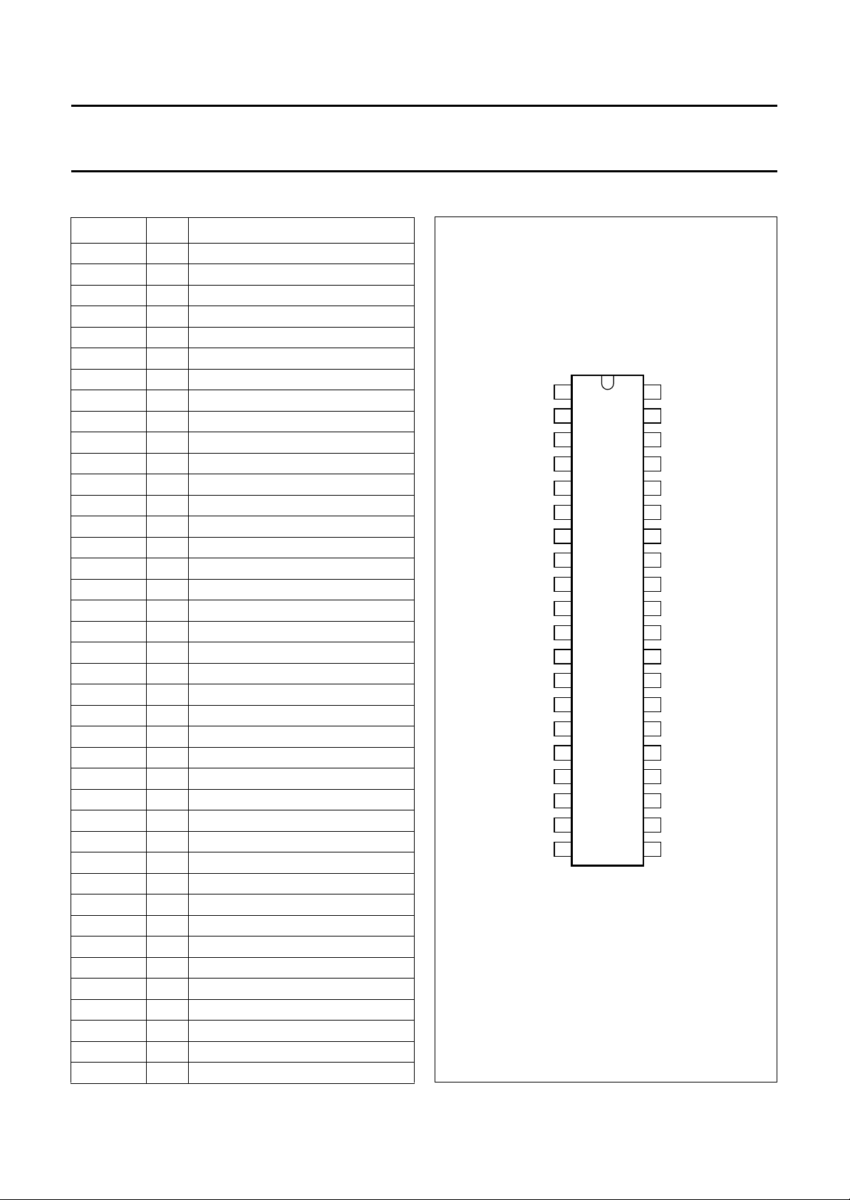
6.3 PCF2112C
SYMBOL PIN DESCRIPTION
CLB 1 clock burst input (CBUS)
V
DD
OSC 3 oscillator input
V
SS
S32 5 LCD driver output 32
S31 6 LCD driver output 31
S30 7 LCD driver output 30
S29 8 LCD driver output 29
S28 9 LCD driver output 28
S27 10 LCD driver output 27
S26 11 LCD driver output 26
S25 12 LCD driver output 25
S24 13 LCD driver output 24
S23 14 LCD driver output 23
S22 15 LCD driver output 22
S21 16 LCD driver output 21
S20 17 LCD driver output 20
S19 18 LCD driver output 19
S18 19 LCD driver output 18
S17 20 LCD driver output 17
S16 21 LCD driver output 16
S15 22 LCD driver output 15
S14 23 LCD driver output 14
S13 24 LCD driver output 13
S12 25 LCD driver output 12
S11 26 LCD driver output 11
S10 27 LCD driver output 10
S9 28 LCD driver output 9
S8 29 LCD driver output 8
S7 30 LCD driver output 7
S6 31 LCD driver output 6
S5 32 LCD driver output 5
S4 33 LCD driver output 4
S3 34 LCD driver output 3
S2 35 LCD driver output 2
S1 36 LCD driver output 1
n.c. 37 not connected
BP 38 backplane driver output
DATA 39 data input line (CBUS)
DLEN 40 data input line enable (CBUS)
2 supply voltage
4 supply voltage ground
handbook, halfpage
CLB
V
DD
OSC
V
SS
S32
S31
S30
S29
S28
S27
S26
S25
S24
S23
S22
S21
S20
S19
S18
S17
1
2
3
4
5
6
7
8
9
10
PCF2112C
11
12
13
14
15
16
17
18
19
20
MLD292
40
DLEN
39
DATA
38
BP
37
n.c.
S1
36
S2
35
34
S3
33
S4
32
S5
31
S6
30
S7
S8
29
S9
28
S10
27
26
S11
25
S12
S13
24
S14
23
S15
22
21
S16
Fig.6 Pin configuration; SOT129-1 and SOT158-1.
1997 Mar 28 8
 Loading...