

Philips PCE84C886P-023, PCE84C886P-077 Datasheet

DATA SH EET
Preliminary specification
File under Integrated Circuits, IC14
1996 Jan 08
INTEGRATED CIRCUITS
PCE84C886
Microcontroller for monitor OSD
and auto-sync applications

1996 Jan 08 2
Philips Semiconductors Preliminary specification
Microcontroller for monitor OSD
and auto-sync applications
PCE84C886
CONTENTS
1 FEATURES
1.1 General
1.2 Special
1.3 OSD
2 GENERAL DESCRIPTION
3 ORDERING INFORMATION
4 BLOCK DIAGRAM
5 PINNING INFORMATION
5.1 Pinning
5.2 Pin description
6 RESET
6.1 Reset trip level
6.2 Reset status
7 ANALOG (DC) CONTROL
7.1 6 and 7-bit PWM outputs
7.2 14-bit PWM output
7.3 A typical PWM output application
8 ANALOG-TO-DIGITAL CONVERTER (ADC)
8.1 Conversion algorithm
9 ON SCREEN DISPLAY (OSD)
9.1 Horizontal starting position control
9.2 Vertical starting position control
9.3 On-chip clock generator
10 DISPLAY RAM ORGANIZATION
10.1 Description of display RAM codes
10.2 Default values of OSD after Power-on-reset
10.3 Loading character data into display RAM
10.4 Writing character data into display RAM
11 CHARACTER ROM
11.1 Character ROM address map
11.2 Character ROM organization
11.3 Combination of character font cells
12 OSD CONTROL REGISTERS
12.1 Derivative Register 22
12.2 Derivative Register 23
12.3 Derivative Register 33
12.4 Derivative Register 34
12.5 Derivative Register 35
12.6 Derivative Register 36
12.7 Derivative Register 37
13 TO FORMAT THE OSD
13.1 Number of characters per row
13.2 Number of rows per frame
13.3 Character size selection for different display
resolutions
14 8-BIT COUNTER (T3)
15 I2C-BUS INTERFACE
16 OUTPUT PORTS
16.1 Mask options
17 DERIVATIVE REGISTERS
18 LIMITING VALUES
19 DC CHARACTERISTICS
20 AC CHARACTERISTICS
21 DEVELOPMENT SUPPORT
22 PACKAGE OUTLINE
23 SOLDERING
23.1 Introduction
23.2 Soldering by dipping or by wave
23.3 Repairing soldered joints
24 DEFINITIONS
25 LIFE SUPPORT APPLICATIONS
26 PURCHASE OF PHILIPS I2C COMPONENTS

1996 Jan 08 3
Philips Semiconductors Preliminary specification
Microcontroller for monitor OSD
and auto-sync applications
PCE84C886
1 FEATURES
1.1 General
• CMOS 8-bit CPU (enhanced 8048 CPU) with 8 kbytes
system ROM and 192 bytes system RAM
• One 8-bit timer/event counter (T1) and one 8-bit counter
triggered by external input (T3)
• Four single level vectored interrupt sources: external
(INTN), counter/timer, I
2
C-bus and VSYNCN
• 2 directly testable inputs T0 and T1
• On-chip oscillator clock frequency: 1 to 10 MHz
• On-chip Power-on-reset with low power detector
• Twelve quasi-bidirectional I/O lines, configuration of
each I/O line individually selected by mask option
• Idle and Stop modes for reduced power consumption
• Operating temperature: −25 to +85 °C
• Operating voltage: 4.5 to 5.5 V
• Package: SDIP42.
1.2 Special
• Master-slave I
2
C-bus interface
• Four 6-bit Pulse Width Modulated outputs
(PWM4 to PWM7)
• Four 7-bit Pulse Width Modulated outputs
(PWM0 to PWM3)
• One 14-bit Pulse Width Modulated output (PWM8)
• Three 4-bit ADC channels
• 16 derivative I/O ports.
1.3 OSD
• Maximum dot frequency (f
OSD
): 14 MHz
• Display RAM: 64 × 10 bits
• Display character fonts: 62 + 2 special reserved codes
• Character matrix: 12 × 18 (no spacing between
characters)
• 4 character sizes: 1H/1V, 1H/2V, 1H/3V and 1H/4V
• 64 Horizontal starting positions (4 dots for each step)
• 64 Vertical starting positions (4 scan lines for each step)
• Spacing between character rows: 0, 4, 8 and 12 scan
lines
• Foreground colours: 8 on a character-by-character
basis
• Background colours: 8 on a word-by-word basis
• Background/shadowing modes: 4 modes available, No
background, North shadowing, Box shadowing and
Frame shadowing (raster blanking) on a frame basis
• On-chip Phase-Locked Loop (PLL) oscillator (auto-sync
with HSYNCN) with programmable oscillator for On
Screen Display (OSD) function
• Character blinking frequency: programmable using
f
Vsync
divisors of 16, 32, 64 and 128; on a frame basis
• Character blinking ratios: 1 : 1, 1 : 3 and 3 : 1
• Programmable active level polarities of VSYNCN,
HSYNCN, R, G, B and FB
• Flexible display format by using Carriage Return Code
• Auto display RAM address (DCRAR) incremented after
write operation to the Character Data Register (DCRCR)
• VSYNCN generates an interrupt (enabled by software)
when VIEN is active.
2 GENERAL DESCRIPTION
The PCE84C886 is a member of the 84CXXX CMOS
microcontroller family. It is suitable for use in 14", 15" and
17" auto-sync monitors for OSD and auto-sync
applications. The device uses the PCE84CXX processor
core and has 8 kbytes of ROM and 192 bytes of RAM. I/O
requirements are adequately catered for with 12 general
purpose bidirectional I/O lines plus 16 function combined
I/O lines. 9 PWM analog outputs are provided specifically
for analog control purposes and also three 4-bit ADCs. The
device has an 8-bit counter, suitable for use in pulse
counting applications; an 8-bit timer/counter with
programmable clock and an on-chip programmable PLL
oscillator that generates the OSD clock. In addition to all
these features a master-slave I
2
C-bus interface, 2 directly
testable lines and an enhanced OSD facility for flexible
screen format (64 character types) are also provided.
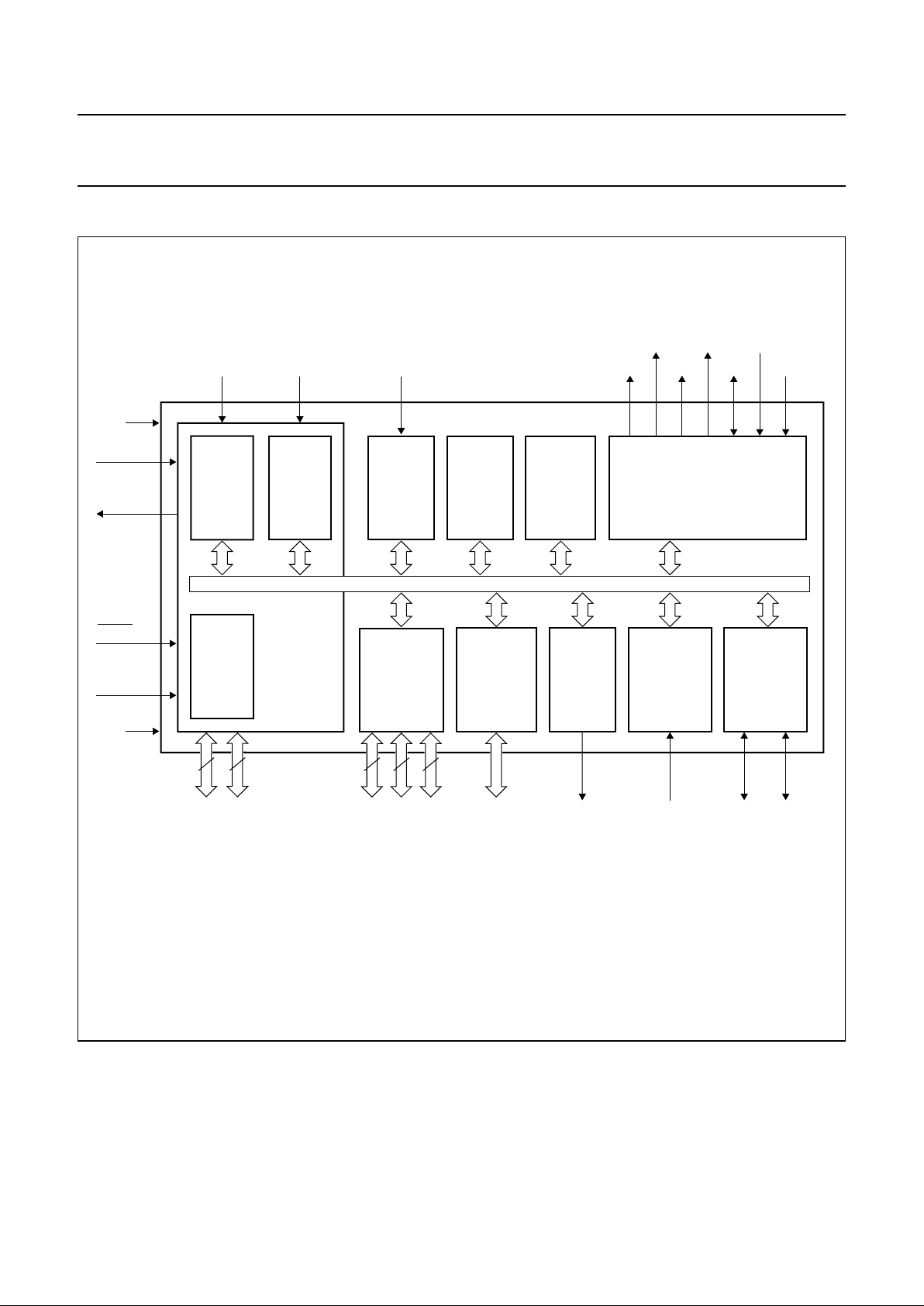
The block diagram of the PCE84C886 is shown in Fig.1.
3 ORDERING INFORMATION
TYPE NUMBER
PACKAGE
NAME DESCRIPTION VERSION
PCE84C886 SDIP42 plastic shrink dual in-line package; 42 leads (600 mil) SOT270-1
1996 Jan 08 4
Philips Semiconductors Preliminary specification
Microcontroller for monitor OSD
and auto-sync applications
PCE84C886
4 BLOCK DIAGRAM
Fig.1 Block diagram.
handbook, full pagewidth
PCF84CXX
core
excluding
ROM / RAM
8-bit internal bus
8-BIT
TIMER /
EVENT
COUNTER
CPU
PARALLEL
I / O
PORTS
8-BIT
COUNTER
ROM
8 kbytes
4 x 6-BIT PWM
4 x 7-BIT PWM
3 x 4-BIT
ADC
I C-BUS
INTERFACE
2
ON SCREEN DISPLAY
4
P0
V
SS
P1
DP0 DP1 DP2
PWM0
to
PWM7
FB
VOW0
VOW1
VOW2CVSYNCN
HSYNCN
V
DD
TEST / EMU
XTAL1 (IN)
XTAL2 (OUT)
RESET
14-BIT
PWM
RAM
192 bytes
PWM8 ADC0
to
ADC2
SDA SCL
MLC067
T1
INTN / T0 T3
8-BIT
I / O
PORTS
48 4
8
(1) (2) (2) (3)
(3) (3)
(3)
(1) Alternative function of DP0.
(2) Alternative function of DP1.
(3) Alternative function of DP2.
1996 Jan 08 5
Philips Semiconductors Preliminary specification
Microcontroller for monitor OSD
and auto-sync applications
PCE84C886
5 PINNING INFORMATION
5.1 Pinning
Fig.2 Pin configuration.
handbook, halfpage
MLC068
1
2
3
4
5
6
7
8
9
10
11
12
13
14
15
16
17
18
19
20
21
42
41
40
39
38
37
36
35
34
33
32
31
30
29
28
27
26
25
24
23
22
HSYNCN
VSYNCN
VOW0/DP23
VOW1/DP22
VOW2
FB
DP13/PWM8
P10
P11
P12
T3
P14
P00
P01
P02
P03
P04
P05
P06
P07
V
SS
PCE84C886
C
DP20/SDA
DP21/SCL
DP10/ADC0
DP11/ADC1
DP12/ADC2
INTN/T0
T1
XTAL2 (OUT)
XTAL1 (IN)
TEST/EMU
DP01/PWM1
DP03/PWM3
DP06/PWM6
DP00/PWM0
DP02/PWM2
DP04/PWM4
DP07/PWM7
DP05/PWM5
DD
V
RESET
1996 Jan 08 6
Philips Semiconductors Preliminary specification
Microcontroller for monitor OSD
and auto-sync applications
PCE84C886
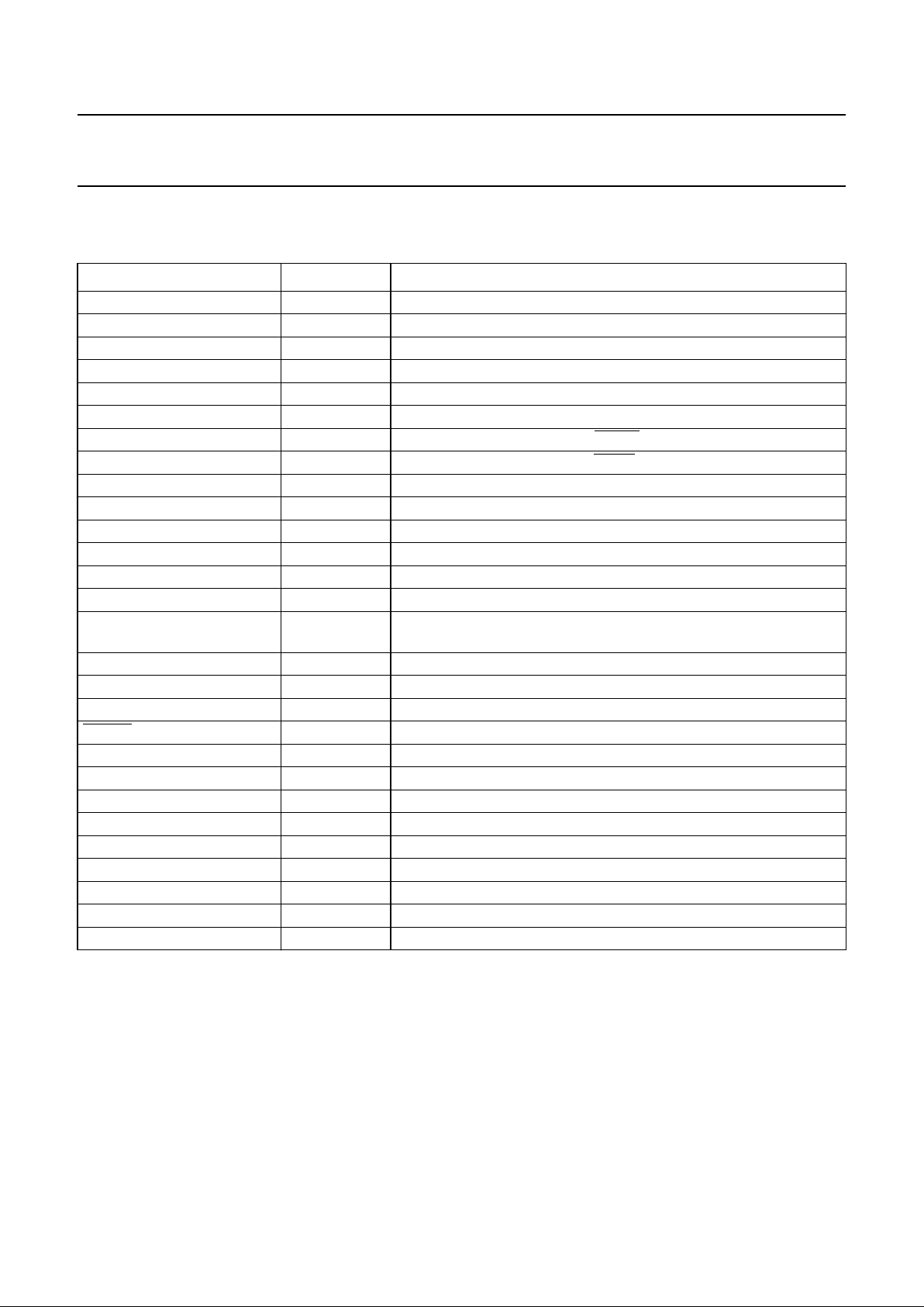
5.2 Pin description
Table 1 SDIP42 package
SYMBOL PIN DESCRIPTION
FB 1 Video Fast Blanking output.
VOW2 2 Video character output VOW2.
VOW1/DP22 3 Video character output VOW1 or Derivative Port line DP22.
VOW0/DP23 4 Video character output VOW0 or Derivative Port line DP23.
VSYNCN 5 Vertical synchronization signal input.
HSYNCN 6 Horizontal synchronization signal input.
P10 7 Port line 10 or emulation input
DXWR.
P11 8 Port line 11 or emulation input
DXRD.
DP13/PWM8 9 Derivative I/O port or PWM8 output.
P12 10 Port line 12 or emulation input DXALE.
T3 11 Secondary 8-bit counter input (Schmitt trigger).
P14 12 Port line 14 or emulation output DXINT.
P00 to P07 13 to 20 General I/O port lines.
V
SS
21 Ground.
DP00/PWM0 to DP07/PWM7 29, 28, 27, 26
25, 24, 23, 22
Derivative I/O ports or PWM outputs.
TEST/EMU 30 Control input for testing and emulation mode, normally LOW.
XTAL1 (IN) 31 Oscillator input pin for system clock.
XTAL2 (OUT) 32 Oscillator output pin for system clock.
RESET 33 Reset input; active LOW input initializes device.
T1 34 Direct testable pin or event counter input.
INTN/T0 35 External interrupt or direct testable pin.
DP10/ADC0 38 Derivative I/O port or ADC Channel 0 input.
DP11/ADC1 37 Derivative I/O port or ADC Channel 1 input.
DP12/ADC2 36 Derivative I/O port or ADC Channel 2 input.
DP21/SCL 39 Derivative port line or I
2
C-bus clock input.
DP20/SDA 40 Derivative port line or I
2
C-bus data input.
C 41 External capacitor input for on-chip oscillator.
V
DD
42 Power supply.
1996 Jan 08 7
Philips Semiconductors Preliminary specification
Microcontroller for monitor OSD
and auto-sync applications
PCE84C886
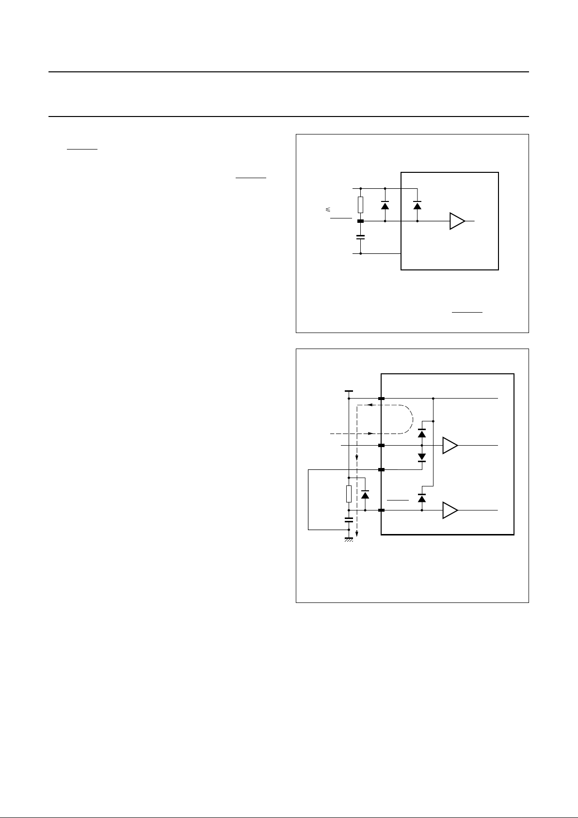
6 RESET
The RESET pin may be used as an active LOW input to
initialize the microcontroller to a defined state.
An active reset can be generated by driving theRESET pin
from an external logic device. Such an active reset pulse
should not fall off before VDD has reached its
f
xtal
-dependent minimum operating voltage.
A Power-on-reset can be generated using an external RC
circuit. To avoid overload of the internal diode, an external
diode should be added in parallel if C
RESET
≥ 2.2 µF. The
RC circuit is shown in Fig.3.
6.1 Reset trip level
The RESET trip voltage level is masked to 1.3 V in the
PCE84C886.
If any input (for example Hsync) goes HIGH before V
DD
is
applied, latch-up may occur and in this situation the
PCE84C886 cannot be reset. The cause and effect of
latch-up is shown in Fig.4.
6.2 Reset status
• Derivative Registers reset status; see Table 38 for
details
• Program Counter 00H
• Memory Bank 0
• Register Bank 0
• Stack Pointer 00H
• All interrupts disabled
• Timer/event counter 1 stopped and cleared
• Timer pre-scaler modulo-32 (PS = 0)
• Timer flag cleared
• Serial I/O interface disabled (ESO = 0) and in slave
receiver mode
• Idle and Stop mode cleared.
Fig.3 External components for RESET pin.
handbook, halfpage
V
V
PCA84C8XX
internal reset
R
C
MLC259
DD
SS
RESET
RESET
RESET
( 100 kΩ)
Fig.4 The influence of an active HIGH signal being
applied before Power-on-reset.
handbook, halfpage
V
V
PCE84C886
internal reset
internal V
R
C
MLC260
DD
DD
V
DD
SS
V
SS
RESET
RESET
Hsync
HSYNCN
RESET
1996 Jan 08 8
Philips Semiconductors Preliminary specification
Microcontroller for monitor OSD
and auto-sync applications
PCE84C886
7 ANALOG (DC) CONTROL
The PCE84C886 has nine Pulse Width Modulated (PWM)
outputs for analog control purposes e.g. brightness,
contrast, H-shift, V-shift, H-width, V-size, E-W, R (or G or
B) gain control etc. Each PWM output generates a pulse
pattern with a programmable duty cycle.
The nine PWM outputs are specified below:
• 4 PWM outputs with 6-bit resolution (PWM4 to PWM7)
• 4 PWM outputs with 7-bit resolution (PWM0 to PWM3)
• 1 PWM output with 14-bit resolution (PWM8).
The 6 and 7-bit PWM outputs are described in Section 7.1;
the 14-bit PWM output is described in Section 7.2 and a
typical PWM output application is described in Section 7.3.
7.1 6 and 7-bit PWM outputs
PWM outputs PWM0 to PWM7 share the same pins as
Derivative Port lines DP00 to DP07 respectively. Selection
of the pin function as either a PWM output or a Derivative
Port line is achieved using the appropriate PWMnE bit in
Register 21 (see Table 38).
The polarity of the PWM outputs is programmable and is
selected by the P7LVL and P6LVL bits in Register 23 (see
Section 12.2).
The duty cycle of outputs PWM0 to PWM7 is dependent
on the programmable contents of the data latches
(Registers 10 to 17 respectively). As the clock frequency
of each PWM circuit is
1
⁄3× f
xtal
, the pulse width of the
pulse generated can be calculated as shown below.
Where (PWMn) is the decimal value held in the data latch.
The maximum repetition frequency (f
PWM
) of the 6 and
7-bit PWM outputs is shown below.
For the 6-bit PWM outputs:
For the 7-bit PWM outputs:
The block diagram for the 6 and 7-bit PWM outputs is
shown in Fig.5.
Pulse width
3 PWMn()×
f
xtal
----------------------------------
=
f
PWM
f
xtal
192
--------- -
=
f
PWM
f
xtal
384
--------- -
=
Fig.5 Block diagram for 6 and 7-bit PWMs.
handbook, full pagewidth
MLC069
DP0x data
I/O
DP0x/PWMx
6 or 7-BIT PWM DATA LATCH
P6LVL/P7LVL
internal data bus
PWMnE
6 or 7-BIT DAC PWM
CONTROLLER
Q
Q
f
xtal
3
1996 Jan 08 9
Philips Semiconductors Preliminary specification
Microcontroller for monitor OSD
and auto-sync applications
PCE84C886
Fig.6 Typical non-inverted output pulse patterns for 6 or 7-bit PWM outputs.
handbook, full pagewidth
f
64
or
128
1 2 3 m m + 1 m + 2
64
or
128
1
00
01
m
63
or
127
decimal value PWM data latch
MLC261
xtal
3
1996 Jan 08 10
Philips Semiconductors Preliminary specification
Microcontroller for monitor OSD
and auto-sync applications
PCE84C886
7.2 14-bit PWM output
PWM8 shares the same pin as Derivative Port line DP13.
Selection of the pin function as either a PWM output or as
a Derivative Port line is achieved using the PWM8E bit in
Register 22 (see Section 12.1).
The Block diagram for the 14-bit PWM output is shown in
Fig.7 and comprises:
• Two 7-bit latches: PWM8L (Register 18) and PWM8H
(Register 19)
• 14-bit data latch (PWMREG)
• 14-bit counter
• Coarse pulse controller
• Fine pulse controller
• Mixer.
Data is loaded into the 14-bit data latch (PWMREG) from
the two 7-bit data latches (PWM8H and PWM8L) when
either of these data latches is written to. The upper seven
bits of PWMREG are used by the coarse pulse controller
and determine the coarse pulse width; the lower seven bits
are used by the fine pulse controller and determine in
which subperiods fine pulses will be added. The outputs
OUT1 and OUT2 of the coarse and fine pulse controllers
are ‘ORED’ in the mixer to give the PWM8 output. The
polarity of the PWM8 output is programmable and is
selected by the P8LVL bit in Register 23, this is described
in Section 12.2.
As the 14-bit counter is clocked by f
xtal
/3, the repetition
times of the coarse and fine pulse controllers may be
calculated as shown below.
Coarse controller repetition time:
Fine controller repetition time:
Figure 8 shows typical PWM8 outputs, with coarse
adjustment only, for different values held in PWM8H.
Figure 9 shows typical PWM8 outputs, with coarse and
fine adjustment, after the coarse and fine pulse controller
outputs have been ‘ORED’ by the mixer.
t
sub
384
f
xtal
--------- -
=
t
r
49152
f
xtal
----------------
=
7.2.1 C
OARSE ADJUSTMENT
An active HIGH pulse is generated in every subperiod; the
pulse width being determined by the contents of PWM8H.
The coarse output (OUT1) is LOW at the start of each
subperiod and will remain LOW until the time
has elapsed. The output will
then go HIGH and remain HIGH until the start of the next
subperiod. The coarse pulse width may be calculated as
shown below.
7.2.2 F
INE ADJUSTMENT
Fine adjustment is achieved by generating an additional
pulse in specific subperiods. The pulse is added at the
start of the selected subperiod and has a pulse width of
3/f
xtal
. The contents of PWM8L determine in which
subperiods a fine pulse will be added. It is the logic 0 state
of the value held in PWM8L that actually selects the
subperiods. When more than one bit is a logic 0 then the
subperiods selected will be a combination of those
subperiods specified in Table 2. For example, if
PWM8L = 111 1010 then this is a combination of:
• PWM8L = 111 1110: subperiod 64 and
• PWM8L = 111 1011: subperiods 16, 48, 80 and 112.
Pulses will be added in subperiods 16, 48, 64, 80 and 112.
This example is illustrated in Fig.10.
When PWM8L holds 111 1111 fine adjustment is inhibited
and the PWM8 output is determined only by the contents
of PWM8H.
Table 2 Additional pulse distribution
PWM8L ADDITIONAL PULSE IN SUBPERIOD
111 1110 64
111 1101 32 and 96
111 1011 16, 48, 80 and 112
111 0111 8, 24, 40, 56, 72, 88, 104 and 120
110 1111 4, 12, 20, 28, 36, 44, 52...116 and 124
101 1111 2, 6, 10, 14, 18, 22, 26, 30...122 and 126
011 1111 1, 3, 5, 7, 9, 11, 13, 15, 17...125 and 127
3f
xtal
⁄ PWM8H 1+()×[]
Pulse duration 127 PWM8H–()
3
f
xtal
--------
×=
1996 Jan 08 11
Philips Semiconductors Preliminary specification
Microcontroller for monitor OSD
and auto-sync applications
PCE84C886
Fig.7 14-bit PWM Block diagram.
handbook, full pagewidth
PWM8L
PWM8H
PWMREG
‘MOVE instruction’
‘MOV instruction’
DATA LOAD
TIMING PULSE
COARSE 7-BIT
PWM
FINE PULSE
GENERATOR
OUT2OUT1
MIXER
Q
Q
P8LVL
14-BIT COUNTER
Q14 to 8 Q7 to 1
polarity
control bit
PWM8 output
f = f
tdac xtal
MLC071
7 7
7 7
LOAD
Internal data bus
3
1996 Jan 08 12
Philips Semiconductors Preliminary specification
Microcontroller for monitor OSD
and auto-sync applications
PCE84C886
Fig.8 Non-inverted PWM8 output patterns - Coarse adjustment only.
handbook, full pagewidth
127 0 1 2 m m + 1 m + 2
127 0 1
00
01
m
127
decimal value PWM8H data latch
MLC263
f
xtal
3
Fig.9 Non-inverted PWM8 output patterns - Coarse and Fine adjustment.
handbook, full pagewidth
f
127 0 1 2 m m + 1 m + 2
127 0 1
00
01
m
127
decimal value PWM8H data latch
MLC262
xtal
3
1996 Jan 08 13
Philips Semiconductors Preliminary specification
Microcontroller for monitor OSD
and auto-sync applications
PCE84C886
Fig.10 Fine adjustment output (OUT2).
handbook, full pagewidth
MLC755
t
sub0
t
sub16
t
sub32
t
sub48
t
sub64
t
sub80
t
sub96
t
sub112
t
sub127
t
r
111 1110
111 1011
111 1010
PWM8L
7.3 A typical PWM output application
A typical PWM application is shown in Fig.11. The buffer is
used to reduce jitter on the OSD. R1 and C1 form the
integration network the time constant of which should be
equal to or greater than 5 times the repetition period of the
PWM output pattern. In order to smooth a changing PWM
output a high value of C1 should be chosen. The value of
C1 will normally be in the range 1 to 10 µF. The potential
divider chain formed by R2 and R3 is used only when the
output voltage is to be offset. The output voltages for this
application are calculated using Equations (1) and (2).
(1)
(2)
The loop from the PWM pin through R1 and C1 to V
SS
will
radiate high frequency energy pulses. In order to limit the
effect of this unwanted radiation source, the loop should
be kept short and a high value of R1 selected. The value
of R1 will normally be in the range 3.3 to 100 kΩ. It is good
practice to avoid sharing VSS (pin 21) with the return leads
of other sensitive signals.
V
max
R3 supply voltage×
R3
R1 R2×
R1 R2+
----------------------
+
----------------------------------------------------
=
V
min
R1 R3×
R1 R3+
--------------------- -
supply voltage×
R2
R1 R3×
R1 R3+
----------------------
+
------------------------------------------------------------------ -
=
Fig.11 Typical PWM output circuit.
handbook, halfpage
MLC070
C1 R3
R1
R2
PCE84C886
PWMn
V
SS
supply
voltage
analog
output
1996 Jan 08 14
Philips Semiconductors Preliminary specification
Microcontroller for monitor OSD
and auto-sync applications
PCE84C886
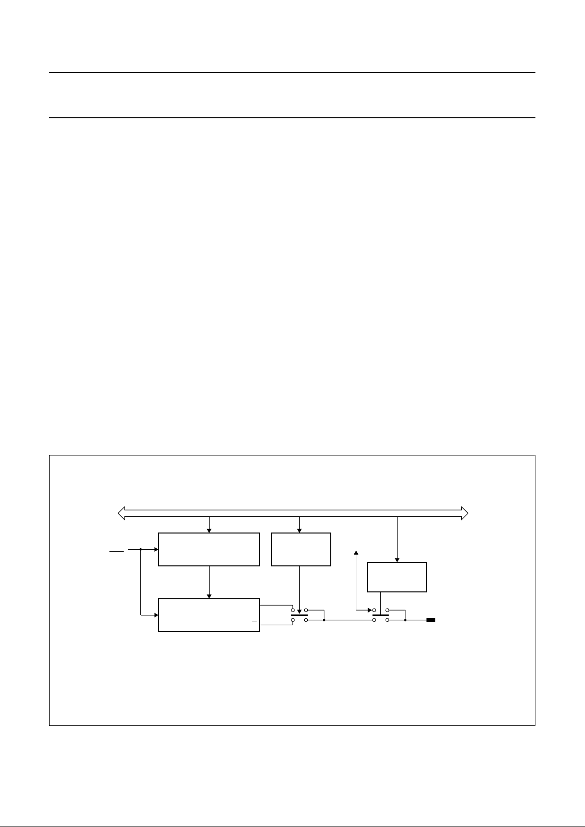
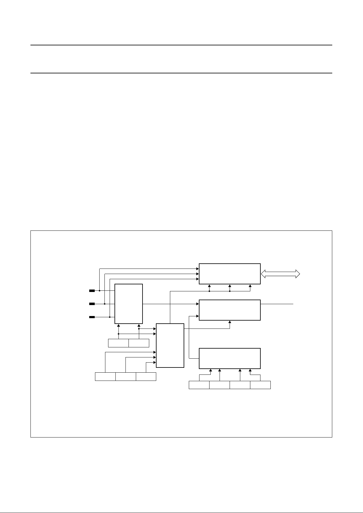
8 ANALOG-TO-DIGITAL CONVERTER (ADC)
The 3 channel ADC comprises a 4-bit Digital-to-Analog
Converter (DAC); a comparator; an analog channel
selector and control circuitry. As the digital input to the 4-bit
DAC is loaded by software (a subroutine in the program),
it is known as a software ADC. The block diagram is shown
in Fig.12.
The ADC inputs ADC0 to ADC2 share the same pins as
Derivative Port lines DP10 to DP12 respectively. Selection
of the pin function as either an ADC input or as a Derivative
Port line is achieved using bits ADCE0 to ADCE2 in
Register 22. When ADCEn = 1, the ADC function is
enabled (see Section 12.1).
The 4-bit DAC analog output voltage (V
ref
) is determined
by the decimal value of the data held in bits DAC0 to DAC3
of Register 20. V
ref
is calculated as shown in Equation (3)
and Table 3 lists the V
ref
values assuming VDD=5V.
(3)
When the analog input voltage is higher than V
ref
, the
COMP bit in Register 20 will be HIGH.
Table 3 Selection of V
ref
DAC3 DAC2 DAC1 DAC0 V
ref
(V)
00000.3125
00010.6250
00100.9375
00111.2500
01001.5625
01011.8750
01102.1875
01112.5000
10002.8125
10013.1250
10103.4375
10113.7500
11004.0625
11014.3750
11104.6875
11115.0000
V
ref
V
DD
16
----------
DAC value 1+()×=
The channel selector, consisting of three analog switches,
is controlled by bits ADCS1 and ADCS0 in Register 20 as
highlighted in Table 4.
Table 4 Selection of ADC channel
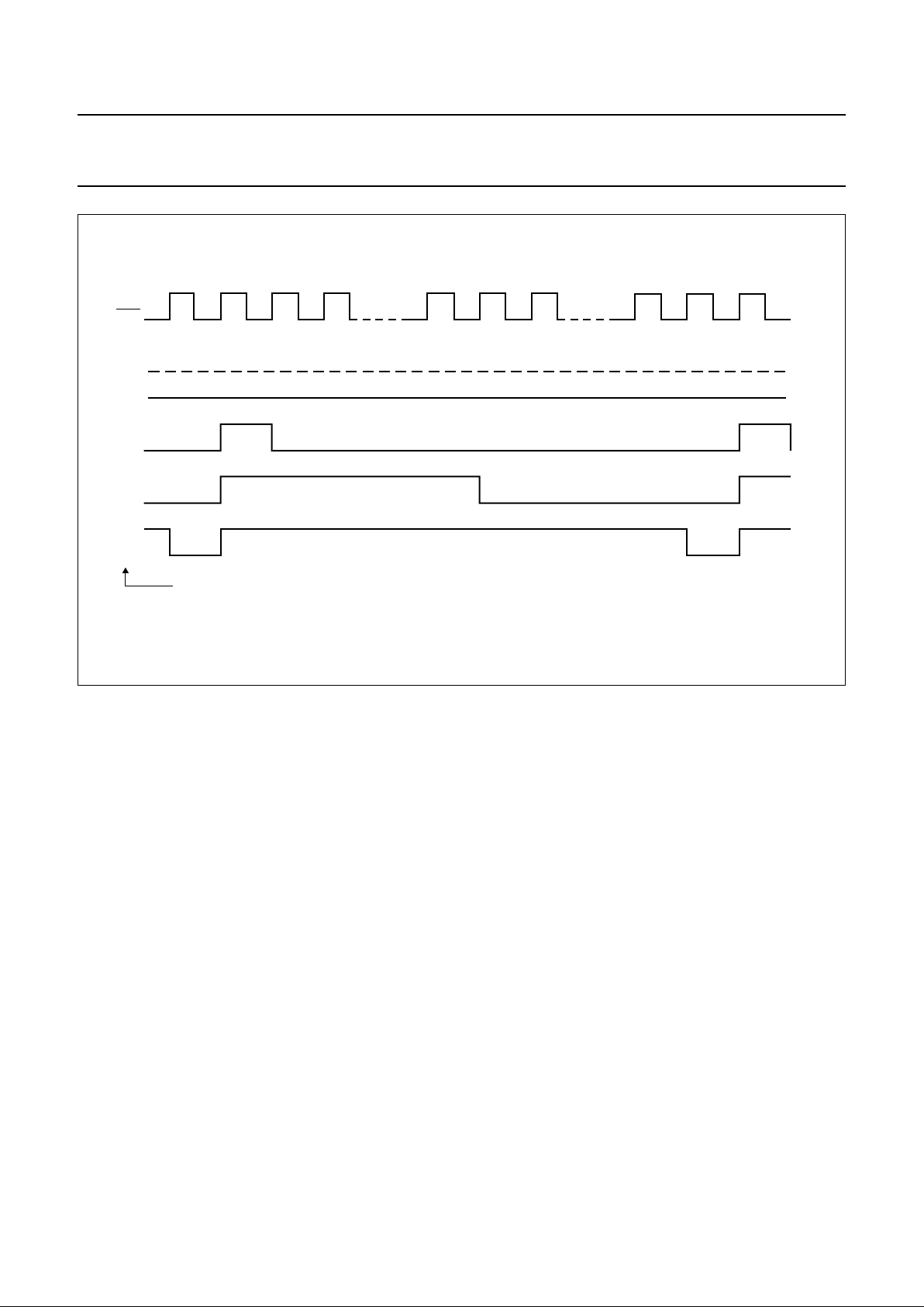
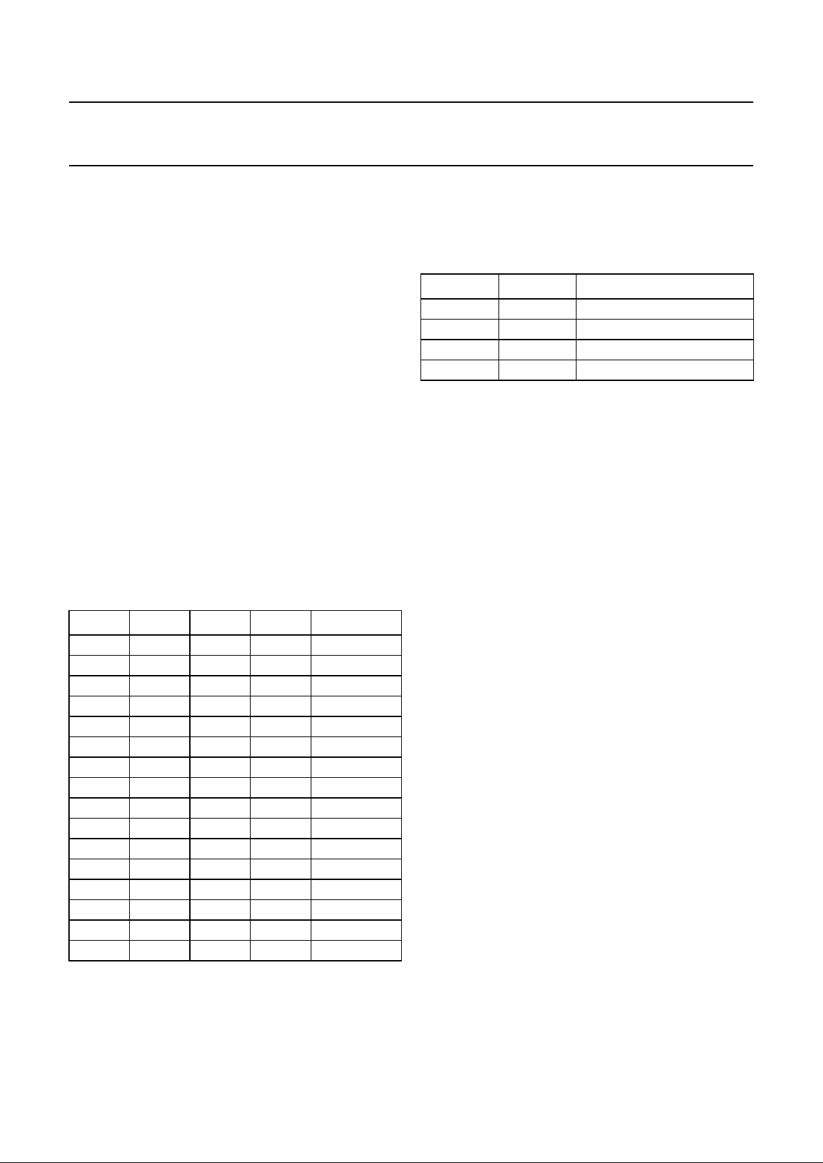
8.1 Conversion algorithm
There are many algorithms available to achieve the ADC
conversion. The algorithm described below and shown in
Fig.13 uses an iteration process.
1. Select ADCn channel for conversion. Channel
selection is achieved using bits ADCS1 and ADCS0 in
Register 20.
2. Set the digital input to the DAC to 1000. The digital
input to the DAC is selected using bits DAC3 to DAC0
in Register 20.
3. Determine the result of the compare operation. This is
achieved by reading the COMP bit in Register 20
using the instruction MOV A, D20. If COMP = 1; the
analog input voltage is higher than the reference
voltage (V
ref
). If COMP = 0; the analog input voltage is
lower than the reference voltage (V
ref
).
4. If COMP = 1; then the analog input voltage is higher
than the reference voltage (V
ref
) and therefore the
digital input to the DAC needs to be increased. Set the
input to the DAC to 1100.
5. If COMP = 0; then the analog input voltage is lower
than the reference voltage (V
ref
) and therefore the
digital input to the DAC needs to be decreased. Set the
input to the DAC to 0100.
6. Determine the result of the compare operation by
reading the COMP bit in Register 20.
ADCS1 ADCS0 CHANNEL SELECTED
0 0 ADC0
0 1 ADC1
1 0 ADC2
1 1 reserved
1996 Jan 08 15
Philips Semiconductors Preliminary specification
Microcontroller for monitor OSD
and auto-sync applications
PCE84C886
7. For the DAC = 1100 case
If COMP = 1; then the analog input voltage is still
greater than V
ref
and therefore the digital input to the
DAC needs to be increased again. Set the input to the
DAC to 1110.
If COMP = 0; then the analog input voltage is now less
than V
ref
and therefore the digital input to the DAC
needs to be decreased. Set the input to the DAC to
1010
8. For the DAC = 0100 case
If COMP = 1; then the analog input voltage is now
greater than V
ref
and therefore the digital input to the
DAC needs to be increased. Set the input to the DAC
to 0110.
If COMP = 0; then the analog input voltage is still lower
than V
ref
and therefore the digital input to the DAC
needs to be decreased again. Set the input to the DAC
to 0010.
9. The operations detailed in 6, 7 and 8 above are
repeated and each time the digital input to the DAC is
changed accordingly; as dictated by the state of the
COMP bit. The complete process is shown in Fig.13.
Each time the DAC input is changed the number of
values which the analog input can take is reduced by
half. In this manner the actual analog value is honed
into. The value of the analog input (VA) is determined
using Equation (4):
(4)
As the conversion time of each compare operation is
greater than 6 µs but less than 9 µs; a NOP instruction is
recommended to be used in between the instructions that
change the value of V
ref
; select the ADC channel and read
the COMP bit.
V
A
V
DD
16
----------
DAC value 1+()×=
Fig.12 Block diagram of 3 channel ADC.
andbook, full pagewidth
4-BIT DAC
COMPARATOR
DAC3
DAC2 DAC1 DAC0
ADCE0 ADCE1 ADCE2
ADCS1 ADCS0
MLC072
ADC enable selection
DAC value selection
ENABLE
SELECTOR
ADC
CHANNEL
SELECTOR
DP12/ADC2
DP11/ADC1
DP10/ADC0
V
ref
EN
DERIVATIVE PORT
SELECTOR
EN1 EN2EN0
‘MOV A, D20’
instruction
to read COMP bit
COMP bit
Internal bus
Channel selection
+
−
1996 Jan 08 16
Philips Semiconductors Preliminary specification
Microcontroller for monitor OSD
and auto-sync applications
PCE84C886
handbook, full pagewidth
MLC073
Value = 1000
COMP = 1
TF
Value = 1100
COMP = 1
TF
Value = 1110
COMP = 1
TF
Value = 1111
COMP = 1
Value = 1101
COMP = 1
TF
1111 1110
TF
1101 1100
Value = 1010
COMP = 1
TF
Value = 1011
COMP = 1
Value = 1001
COMP = 1
TF
1010
TF
1001 10001011
Value = 0100
COMP = 1
TF
Value =0110
COMP = 1
TF
Value = 0111
COMP = 1
Value = 0101
COMP = 1
TF
0111 0110
TF
0101 0100
Value = 0010
COMP = 1
TF
Value = 0011
COMP = 1
Value = 0001
COMP = 1
TF
0010
TF
00010011
0000
Fig.13 Example of converting algorithm for software ADC.

1996 Jan 08 17
Philips Semiconductors Preliminary specification
Microcontroller for monitor OSD
and auto-sync applications
PCE84C886
9 ON SCREEN DISPLAY (OSD)
The OSD feature of the PCE84C886 enables the user to
display information on the monitor screen. Display
information can be created using 62 customer designed
characters, a space character and a carriage return code.
The OSD block diagram is shown in Fig.14.
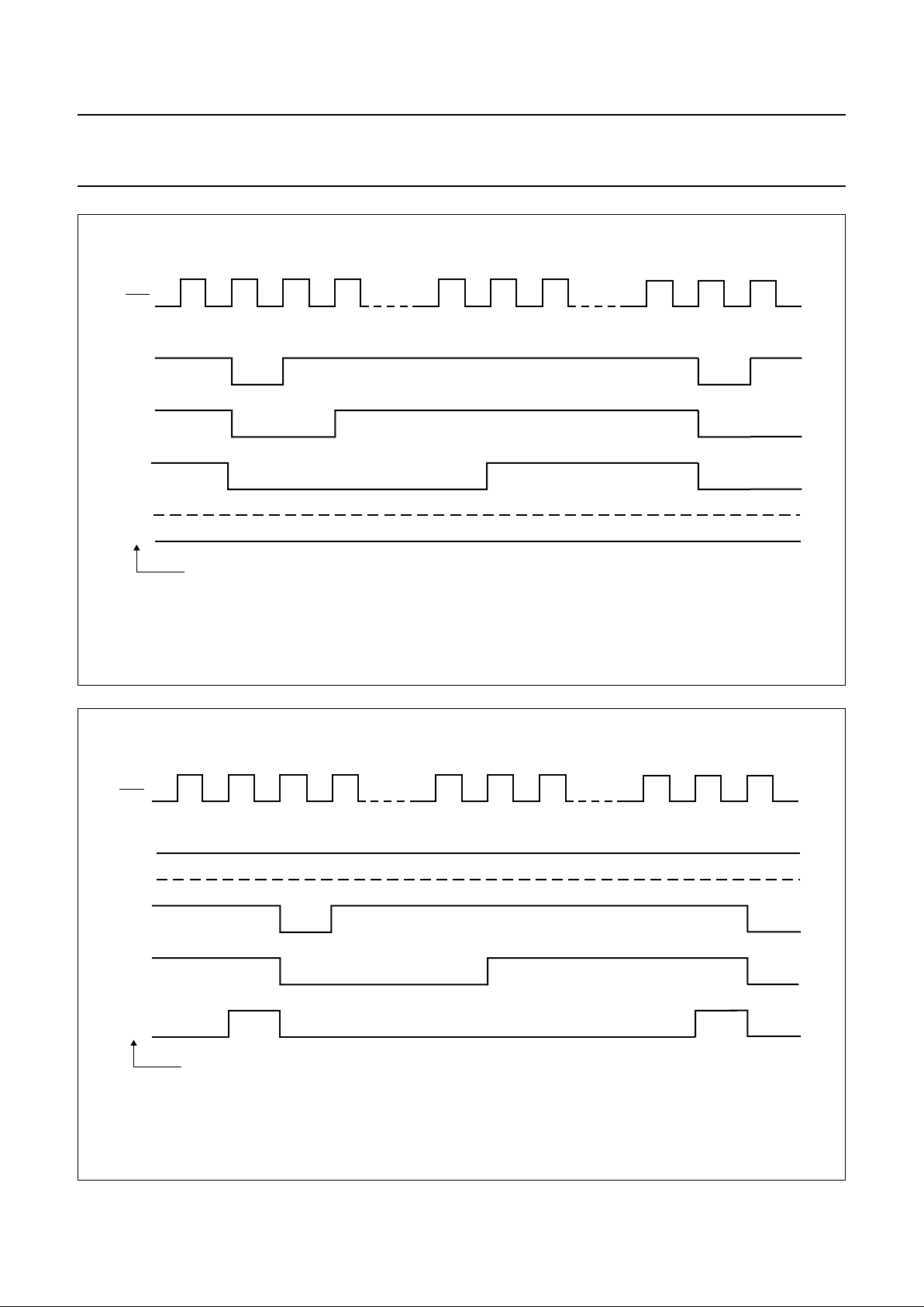
9.1 Horizontal starting position control
The horizontal starting position counter is incremented
every OSD clock after Hsync becomes inactive and is
reset when Hsync becomes active. The horizontal starting
position of the display row is determined by the contents of
Register 36; 1 of 64 positions may be selected as
explained in Section 12.6.
The polarity of the active state of the HSYNCN input is
programmable and is determined by the Hp bit in
Register 34; see Section 12.4. The active HIGH and active
LOW states as selected by the Hp bit are shown in Fig.15.
9.2 Vertical starting position control
The vertical starting position counter is incremented every
Hsync cycle and is reset when Vsync becomes active. The
vertical starting position of the display row is determined by
the contents of Register 35; 1 of 64 positions may be
selected as explained in Section 12.5.
The vertical starting position of the display is dependent
upon the number of scan lines per frame. To achieve the
same starting position with different display resolutions,
only the contents of Register 35 need to be changed, the
contents of Register 36 remain the same. The lowest
vertical starting position that can be selected, is located on
the 256th scan-line. However, lower positions may be
achieved using the Carriage Return Code.
When the selected horizontal and vertical starting
positions are reached on screen; the OSD is enabled. The
character selected in display RAM is then displayed.
The polarity of the active state of the VSYNCN input is
programmable and is determined by the Vp bit in Register
34; see Section 12.4. The active HIGH and active LOW
states as selected by the Vp bit are shown in Fig.15.
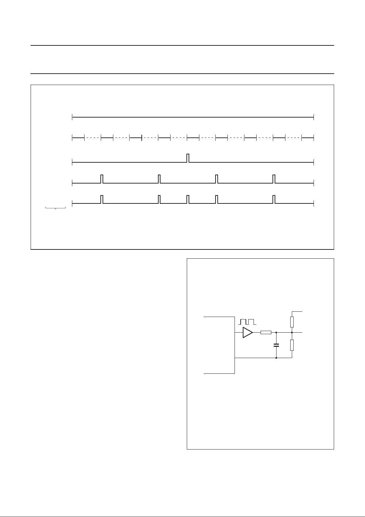
9.3 On-chip clock generator
The on-chip oscillator generates an OSD clock that is
auto-sync with Hsync. The frequency of the OSD clock is
programmable and is determined by the contents of
Register 25 which forms the 7-bit counter.
The OSD clock frequency is calculated as follows:
Where (Register 25) denotes the decimal value held in
Register 25.
The block diagram of the OSD clock is shown in Fig.16.
The internal reference frequency is connected to Hsync,
and if the frequency of Hsync changes, the output
frequency (f
OSD
) will be changed linearly. Therefore, the
character width is not effected by changes in the frequency
of Hsync. The internal Hsync signal is designed active
HIGH, consequently f
PLL
is synchronized with the falling
edge of this signal.
The OSD clock is enabled/disabled by the state of the EN
bit in Register 34; see Section 12.4. When the OSD clock
is disabled the oscillator remains active, therefore the
transient time from the OSD clock start-up to locking into
the external Hsync signal is reduced. As the on-chip
oscillator is always active after power-on, when the OSD
clock is enabled no large currents flow (as in the case of
RC or LC oscillators) and therefore radiated noise is
dramatically reduced.
f
OSDfHsync
2 Register 25()××=
 Loading...