

Philips PCE84C48 Service Manual

INTEGRATED CIRCUITS
DATA SH EET
PCE84C486; PCE84C487
Microcontrollers for digital
auto-sync and VST TV controller
applications
Objective specification
File under Integrated Circuits, IC14
1996 Feb 21

Philips Semiconductors Objective specification
Microcontrollers for digital auto-sync
and VST TV controller applications
CONTENTS
1 FEATURES
1.1 General
1.2 Special
2 GENERAL DESCRIPTION
3 ORDERING INFORMATION
4 BLOCK DIAGRAMS
5 PINNING INFORMATION
5.1 Pinning
5.2 Pin description
6 RESET
6.1 External reset using the RESET pin
6.2 Power-on-reset
6.3 Watchdog Timer reset
6.4 Reset trip level
6.5 Reset status
7 ANALOG (DC) CONTROL
7.1 6 and 7-bit PWM outputs
7.2 8-bit PWM outputs
7.3 14-bit PWM output (PWM8)
7.4 A typical PWM output application
8 ANALOG-TO-DIGITAL CONVERTER (ADC)
8.1 Conversion algorithm
8.2 A typical application for keypad detection
9I
10 8-BIT COUNTER (T3)
11 WATCHDOG TIMER (WDT)
12 OUTPUT PORTS
12.1 Mask options
13 DERIVATIVE REGISTERS
2
C-BUS INTERFACE
PCE84C486;
PCE84C487
14 LIMITING VALUES
15 DC CHARACTERISTICS
16 AC CHARACTERISTICS
17 PACKAGE OUTLINES
18 SOLDERING
18.1 Introduction
18.2 SDIP
19 DEFINITIONS
20 LIFE SUPPORT APPLICATIONS
21 PURCHASE OF PHILIPS I2C COMPONENTS
1996 Feb 21 2

Philips Semiconductors Objective specification
Microcontrollers for digital auto-sync and
VST TV controller applications
1 FEATURES
1.1 General
• CMOS 8-bit CPU (enhanced 8048 CPU) with 4 kbytes
system ROM and 128 bytes system RAM
• One 8-bit timer/event counter (T1) and one 8-bit counter
(T3) triggered by external input
• Three single level vectored interrupt sources: external
(INTN), counter/timer and I
• 2 directly testable inputs T0 and T1
• On-chip oscillator clock frequency: 1 to 10 MHz
• On-chip Power-on-reset with low power detector
• The PCE84C486 has eleven quasi-bidirectional I/O
lines, the PCE84C487 has twelve. The configuration of
each I/O line individually selected by mask option
• Idle and Stop modes for reduced power consumption
• Operating temperature: −25 to +85 °C
• Operating voltage: 4.5 to 5.5 V
• Packages: SDIP32 for the PCE84C486; SDIP42 for the
PCE84C487.
1.2 Special
2
• Master-slave I
• Four 6-bit Pulse Width Modulated outputs
• Four 7-bit Pulse Width Modulated outputs
• Four 8-bit Pulse Width Modulated outputs (PCE84C487
only)
• One 14-bit Pulse Width Modulated output
• Two 4-bit Analog-to-Digital Converter (ADC) channels
• 14 derivative I/O ports
• Watchdog Timer.
C-bus interface
2
C-bus
PCE84C486; PCE84C487
2 GENERAL DESCRIPTION
The PCE84C486 and PCE84C487 are low-cost
microcontrollers and have been designed for use with
auto-sync monitors, handling mode detection, digital
control and Voltage Synthesized Tuning (VST). These
microcontrollers have no on-chip OSD function.
The term PCE84C48X is used throughout this data sheet
to refer to both devices. Differences between the
PCE84C486 and the PCE84C487 are highlighted
throughout the document.
The PCE84C48X is a member of the 84CXXX CMOS
microcontroller family. The device uses the PCE84CXX
processor core and has 4 kbytes of ROM and 128 bytes of
RAM. I/O requirements are catered for with 11 general
purpose bidirectional I/O lines (the PCE84C487 has 12)
plus 12 function combined I/O lines (the PCE84C487 has
16). Nine PWM analog outputs (the PCE84C487 has 13)
are available for analog control purposes and also a two
channel 4-bit ADC. The device has an 8-bit counter (T3),
for use in pulse counting applications and also an 8-bit
timer/counter (T1) with programmable clock. A Watchdog
timer, a master-slave I2C-bus interface and 2 directly
testable lines are also available on-chip.
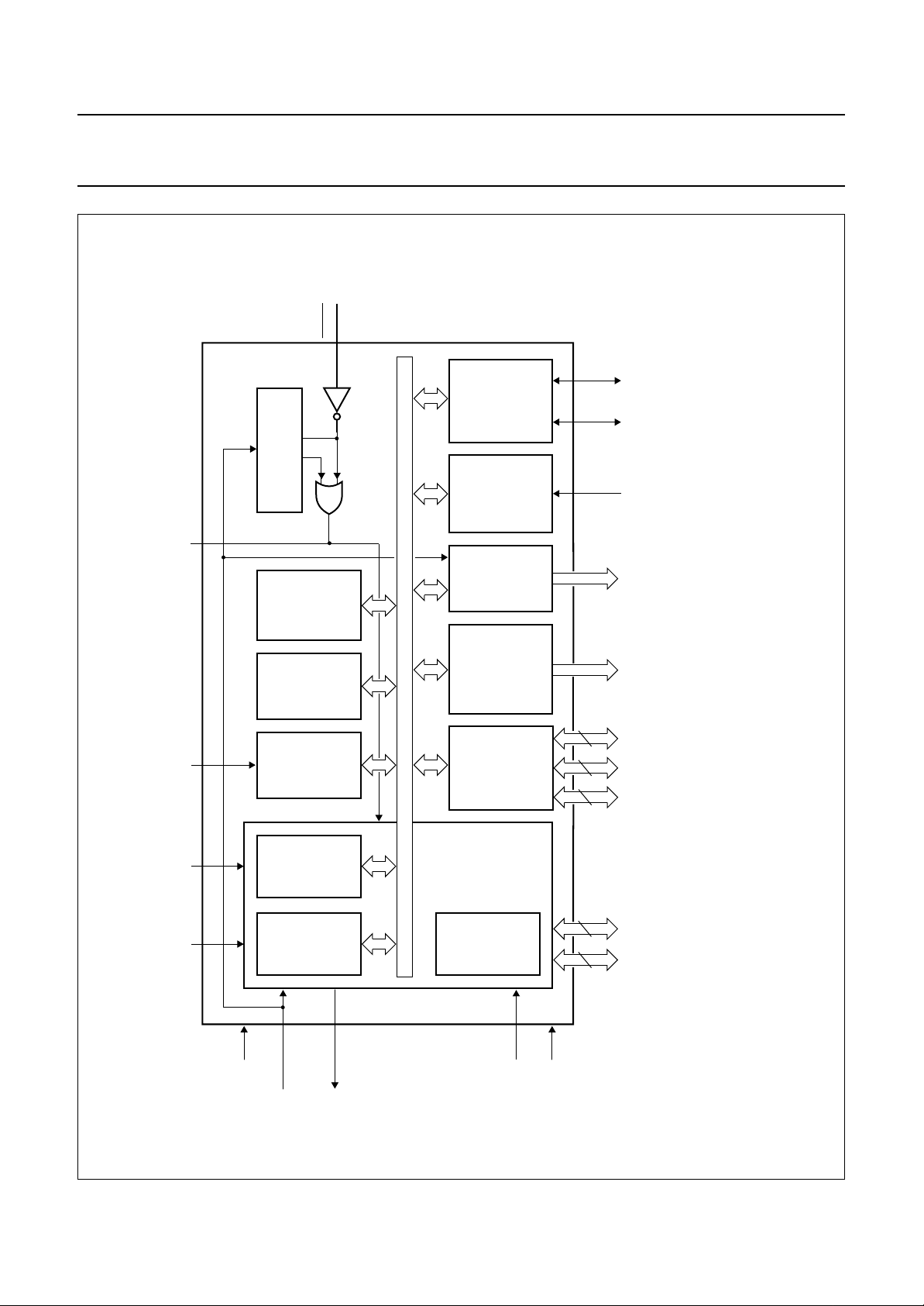
The block diagram of the PCE84C486 is shown in Fig.1;
the block diagram of the PCE84C487 is shown in Fig.2.
3 ORDERING INFORMATION
TYPE NUMBER
NAME DESCRIPTION VERSION
PCE84C486 SDIP32 plastic shrink dual in-line package; 32 leads (400 mil) SOT232-1
PCE84C487 SDIP42 plastic shrink dual in-line package; 42 leads (600 mil) SOT270-1
1996 Feb 21 3
PACKAGE

Philips Semiconductors Objective specification
Microcontrollers for digital auto-sync and
VST TV controller applications
4 BLOCK DIAGRAMS
RESET
8-bit internal bus
WATCHDOG TIMER
2
I C-BUS
INTERFACE
2 x 4-BIT ADC
PCE84C486; PCE84C487
MGC912
SDA SCL
and
ADC1
ADC2
INTN / T0 T3
T1
RAM
128 bytes
ROM
4 kbytes
8-BIT
COUNTER
CPU
8-BIT
TIMER /
EVENT
COUNTER
4 x 6-BIT PWM
4 x 7-BIT PWM
1 x 14-BIT PWM
I / O PORTS
PCF84CXX
core
excluding
ROM / RAM
I / O
PORTS
PARALLEL
EMU
(1) (1) (2) (3)
to
PWM8
PWM0
38
DP1 DP2
DP0
4
P1
8
P0
handbook, full pagewidth
Fig.1 PCE84C486 block diagram.
DD
V
XTAL1 (IN)
XTAL2 (OUT)
1996 Feb 21 4
SS
V
(1) Alternative functions of DP0 and DP1.
(2) Alternative functions of DP2.
(3) Alternative function of P1.
Philips Semiconductors Objective specification
Microcontrollers for digital auto-sync and
VST TV controller applications
RESET
8-bit internal bus
WATCHDOG TIMER
RAM
128 bytes
2
I C-BUS
INTERFACE
2 x 4-BIT ADC
PWM
4 x 8-BIT
PCE84C486; PCE84C487
MGC913
SDA SCL
and
ADC1
ADC2
to
PWM13
PWM10
INTN / T0 T3 RSTO
T1
DD
V
ROM
4 kbytes
8-BIT
COUNTER
CPU
8-BIT
EVENT
TIMER /
XTAL1 (IN)
COUNTER
XTAL2 (OUT)
4 x 6-BIT PWM
4 x 7-BIT PWM
1 x 14-BIT PWM
I / O PORTS
PCF84CXX
core
excluding
I / O
PORTS
PARALLEL
EMU
ROM / RAM
SS
V
(1) (2) (1) (2) (3)
to
PWM8
PWM0
38 5
DP0 DP1 DP2
4
P1
8
P0
handbook, full pagewidth
Fig.2 PCE84C487 block diagram.
1996 Feb 21 5
(1) Alternative functions of DP0 and DP1.
(2) Alternative function of DP2.
(3) Alternative function of P1.

Philips Semiconductors Objective specification
Microcontrollers for digital auto-sync and
VST TV controller applications
5 PINNING INFORMATION
5.1 Pinning
handbook, halfpage
DP13/PWM8
DP20/SDA
P10/SCL
P11
P12
P14
P00
P01
P02
P03
P04
P05
P06
P07
V
T3
SS
1
2
3
4
5
6
7
8
PCE84C486
9
10
11
12
13
14
15
16
MGC904
32
DP07/PWM7
31
DP12/ADC2
30
INTN/T0
29
T1
28
RESET
27
XTAL2(OUT)
26
XTAL1(IN)
25
V
DD
24
DP00/PWM0
23
DP01/PWM1
22
DP02/PWM2
21
DP03/PWM3
20
DP04/PWM4
19
DP05/PWM5
18
DP06/PWM6
17
DP11/ADC1
handbook, halfpage
DP20/SDA
DP13/PWM8
DP24/PWM10
DP25/PWM11
PCE84C486; PCE84C487
P10/SCL
P11
P12
n.c.
T3
P14
P00
RSTO
P01
P02
P03
n.c.
P04
P05
P06
P07
V
SS
1
2
3
4
5
6
7
8
9
10
11
PCE84C487
12
13
14
15
16
17
18
19
20
MGC905
42
DP07/PWM7
41
DP12/ADC2
40
INTN/T0
39
T1
38
RESET
37
n.c.
36
XTAL2(OUT)
35
XTAL1(IN)
34
DP27/PWM13
33
V
DD
32
EMU
31
DP00/PWM0
30
DP01/PWM1
29
DP26/PWM12
28
DP02/PWM2
27
n.c.
26
DP03/PWM3
25
DP04/PWM4
24
DP05/PWM5
23
DP06/PWM6
2221
DP11/ADC1
Fig.3 Pin configuration - PCE84C486.
1996 Feb 21 6
Fig.4 Pin configuration - PCE84C487.

Philips Semiconductors Objective specification
Microcontrollers for digital auto-sync and
PCE84C486; PCE84C487
VST TV controller applications
5.2 Pin description
Table 1 SDIP32 package
SYMBOL PIN DESCRIPTION
DP20/SDA 1 Derivative port line 20 or I
2
P10/SCL 2 Port line 10 or I
P11 3 Port line 11 or emulation input
DP13/PWM8 4 Derivative I/O port 13 or PWM8 output.
P12 5 Port line 12 or emulation input DXALE.
T3 6 8-bit counter input (Schmitt trigger).
P14 7 Port line 14 or emulation output DXINT.
P00 to P07 8 to 15 General I/O port lines.
V
SS
DP11/ADC1 17 Derivative I/O port 11 or ADC Channel 1input.
DP00/PWM0 to DP07/PWM7 24 to 18, 32 Derivative I/O ports or 6 and 7-bit PWM outputs.
V
DD
XTAL1 (IN) 26 Oscillator input pin for system clock.
XTAL2 (OUT) 27 Oscillator output pin for system clock.
RESET 28 Reset input; active LOW input initializes device.
T1 29 Direct testable pin or event counter input.
INTN/T0 30 External interrupt or direct testable pin.
DP12/ADC2 31 Derivative I/O port 12 or ADC Channel 2 input.
16 Ground pin.
25 Power supply.
C-bus clock line or emulation input DXWR.
2
C-bus data line.
DXRD.
1996 Feb 21 7

Philips Semiconductors Objective specification
Microcontrollers for digital auto-sync and
PCE84C486; PCE84C487
VST TV controller applications
Table 2 SDIP42 package
SYMBOL PIN DESCRIPTION
2
DP20/SDA 1 Derivative port line 20 or I
2
P10/SCL 2 Port line 10 or I
P11 3 Port line 11 or emulation input
DP13/PWM8 4 Derivative I/O port 13 or PWM8 output.
P12 5 Port line 12 or emulation input DXALE.
n.c. 6 Not connected.
T3 7 8-bit counter input (Schmitt trigger).
DP24/PWM10 to DP27/PWM13 8, 14, 29, 34 Derivative I/O ports or 8-bit PWM outputs.
P14 9 Port line 14 or emulation output DXINT.
P00 to P07
RSTO 11 Used for emulation purposes only. This active HIGH output is the
n.c. 16 Not connected.
V
SS
DP11/ADC1 22 Derivative I/O port 11 or ADC channel 1 input.
DP04/PWM4 to DP07/PWM7 25, 24, 23, 42 Derivative I/O ports or 6-bit PWM outputs.
n.c. 27 Not connected.
DP00/PWM0 to DP03/PWM3 31, 30, 28, 26 Derivative I/O ports or 7-bit PWM outputs.
EMU 32 Emulation mode control input, normally LOW.
V
DD
XTAL1 (IN) 35 Oscillator input pin for system clock.
XTAL2 (OUT) 36 Oscillator output pin for system clock.
n.c. 37 Not connected.
RESET 38 Reset input; active LOW input initializes device.
T1 39 Direct testable pin or event counter input.
INTN/T0 40 External interrupt or direct testable pin.
DP12/ADC2 41 Derivative I/O port 12 or ADC Channel 2 input.
10, 12, 13, 15,
17, 18, 19, 20
21 Ground pin.
33 Power supply.
General I/O port lines.
result of the OR operation carried out internally on the
input and the Watchdog Timer reset line.
C-bus clock line or emulation input DXWR.
C-bus data line.
DXRD.
RESET
1996 Feb 21 8

Philips Semiconductors Objective specification
Microcontrollers for digital auto-sync and
VST TV controller applications
6 RESET
To initialize the microcontroller to a defined state a reset
operation is performed. A reset can be generated in three
ways:
• applying an external signal to the RESET pin
• via Power-on-reset circuitry
• by the Watchdog Timer.
6.1 External reset using the
An active LOW signal from an external logic device will
reset the device. The signal must be maintained long
enough to allow VDD to reach its f
operating voltage.
6.2 Power-on-reset
A Power-on-reset can be generated using an external RC
circuit. To avoid overload of the internal diode, an external
diode should be added in parallel if C
The RC circuit is shown in Fig.5.
RESET pin
-dependent minimum
xtal
≥ 2.2 µF.
RESET
PCE84C486; PCE84C487
6.4 Reset trip level
The RESET trip voltage level for both the PCE84C486 and
PCE84C487 is masked to 1.3 V.
6.5 Reset status
• Derivative Registers reset status; see Table 8 for details
• Program Counter 00H
• Memory Bank 0
• Register Bank 0
• Stack Pointer 00H
• All interrupts disabled
• Timer/event counter 1 stopped and cleared
• Timer pre-scaler modulo-32 (PS = 0)
• Timer flag cleared
• Serial I/O interface disabled (ESO = 0) and in slave
receiver mode
• Idle and Stop mode cleared.
6.3 Watchdog Timer reset
An overflow of the Watchdog Timer will cause the device
to be reset. The operation of the Watchdog Timer is
described in Chapter 12.
handbook, halfpage
V
DD
R
RESET
( 100 kΩ)
RESET
C
RESET
V
SS
internal reset
PCA84C8XX
MLC259
Fig.5 External components for RESET pin.
1996 Feb 21 9

Philips Semiconductors Objective specification
Microcontrollers for digital auto-sync and
VST TV controller applications
7 ANALOG (DC) CONTROL
The PCE84C486 has nine Pulse Width Modulated outputs
(PWM0 to PWM8) and the PCE84C487 has thirteen Pulse
Width Modulated outputs (PWM0 to PWM8 and
PWM10 to PWM13). These outputs are used for analog
control purposes e.g. brightness, contrast, H-shift, V-shift,
H-width, V-size, pin-cushion, trapezium, R (or G or B) gain
control, sound volume etc. Each PWM output generates a
pulse pattern with a programmable duty cycle.
The PWM outputs are specified below:
• PWM0 to PWM3: 4 PWM outputs with 7-bit resolution
• PWM4 to PWM7: 4 PWM outputs with 6-bit resolution
• PWM8: 1 PWM output with 14-bit resolution
• PWM10 to PWM13: 4 PWM outputs with 8-bit
resolution.
The 6 and 7-bit PWM outputs are described in Section 7.1;
the 8-bit PWM outputs are described in Section 7.2 and
the 14-bit PWM output is described in Section 7.3. A
typical PWM output application is described in Section 7.4.
7.1 6 and 7-bit PWM outputs
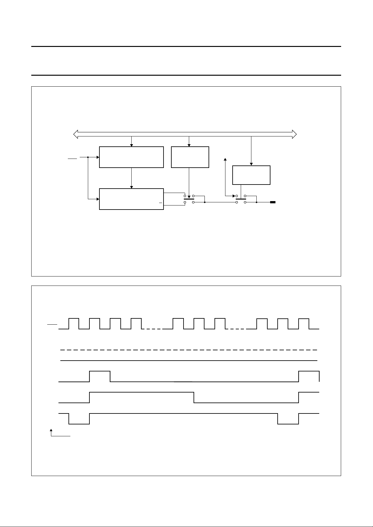
The block diagram for the 6 and 7-bit PWM outputs is
shown in Fig.6.
Pulse Width Modulated outputs PWM0 to PWM7 share
the same pins as Derivative Port lines DP00 to DP07,
respectively. Selection of the pin function as either a PWM
output or a Derivative Port line is achieved using the
appropriate PWMnE bit in the PWME1 Register (see
Table 8).
The polarity of the 6 and 7-bit PWM outputs is
programmable and is selected by the P7LVL or the P6LVL
bit in the CON2 Register (see Table 8). The state of the
P7LVL bit determines the polarity of the 7-bit PWMs; the
state of the P6LVL bit determines the polarity of the 6-bit
PWMs.
The duty cycle of each PWM output is dependent upon the
programmable contents of its associated data latch
(PWM0 to PWM7 Registers respectively). As the clock
frequency of each PWM circuit is
of the pulse generated can be calculated as shown below.
1
⁄3× f
, the pulse width
xtal
PCE84C486; PCE84C487
The maximum repetition frequency (f
7-bit PWM outputs is shown below.
For the 6-bit PWM outputs:
For the 7-bit PWM outputs:
f
PWM
f
PWM
7.2 8-bit PWM outputs
The block diagram for the 8-bit PWM outputs is shown in
Fig.8.
The 8-bit PWM outputs PWM10 to PWM13 (only available
with the PCE84C487) share the same pins as Derivative
Port lines DP24 to DP27, respectively. Selection of the pin
function as either a PWM output or a Derivative Port line is
achieved using the appropriate PWMnE bit in the
PWME2 Register (see Table 8). In the PCE84C486 the
contents of the PWME2 register should be set so that
these PWM outputs are disabled (i.e 00H).
The polarity of the 8-bit PWM outputs is programmable
and is selected by the P8LVL bit in the CON2 Register.
The duty cycle of each 8-bit PWM output is dependent
upon the programmable contents of its associated data
latch (PWM10 to PWM13 Registers respectively). As the
clock frequency of each PWM circuit is f
width of the pulse generated can be calculated as shown
below.
Pulse width
PWMn()
=
-----------------------f
xtal
Where (PWMn) is the decimal value held in the data latch.
The maximum repetition frequency (f
PWM outputs is shown below.
f
PWM
--------- 256
f
xtal
=
An 8-bit PWM output is driven HIGH when the value held
in its data latch is 00H. This is different to the 6 and 7-bit
PWM outputs which are driven LOW when their data
latches contain 00H.
=
=
PWM
f
xtal
--------- 192
f
xtal
--------- 384
PWM
) of the 6 and
, the pulse
xtal
) of the 8-bit
3 PWMn()×
Pulse width
=
---------------------------------f
xtal
Where (PWMn) is the decimal value held in the data latch.
1996 Feb 21 10
Philips Semiconductors Objective specification
Microcontrollers for digital auto-sync and
VST TV controller applications
handbook, full pagewidth
f
xtal
3
6 or 7-BIT PWM DATA LATCH
6 or 7-BIT DAC PWM
CONTROLLER
internal data bus
P6LVL/P7LVL
Q
Q
PCE84C486; PCE84C487
DP0x data
I/O
PWMnE
DP0x/PWMx
MLC069
f
handbook, full pagewidth
xtal
3
64
or
128
00
01
m
63
or
127
Fig.6 Block diagram for 6 and 7-bit PWMs.
1 2 3 m m + 1 m + 2
decimal value PWM data latch
64
or
128
1
MLC261
Fig.7 Typical non-inverted output pulse patterns for 6 or 7-bit PWM outputs.
1996 Feb 21 11
 Loading...