Philips PCD8544U-2-F1 Datasheet

DATA SH EET
Product specification
File under Integrated Circuits, IC17
1999 Apr 12
INTEGRATED CIRCUITS
PCD8544
48 × 84 pixels matrix LCD
controller/driver

1999 Apr 12 2
Philips Semiconductors Product specification
48 × 84 pixels matrix LCD controller/driver PCD8544
CONTENTS
1 FEATURES
2 GENERAL DESCRIPTION
3 APPLICATIONS
4 ORDERING INFORMATION
5 BLOCK DIAGRAM
6 PINNING
6.1 Pin functions
6.1.1 R0 to R47 row driver outputs
6.1.2 C0 to C83 column driver outputs
6.1.3 V
SS1,VSS2
: negative power supply rails
6.1.4 V
DD1,VDD2
: positive power supply rails
6.1.5 V
LCD1,VLCD2
: LCD power supply
6.1.6 T1, T2, T3 and T4: test pads
6.1.7 SDIN: serial data line
6.1.8 SCLK: serial clock line
6.1.9 D/C: mode select
6.1.10 SCE: chip enable
6.1.11 OSC: oscillator
6.1.12 RES: reset
7 FUNCTIONAL DESCRIPTION
7.1 Oscillator
7.2 Address Counter (AC)
7.3 Display Data RAM (DDRAM)
7.4 Timing generator
7.5 Display address counter
7.6 LCD row and column drivers
7.7 Addressing
7.7.1 Data structure
7.8 Temperature compensation
8 INSTRUCTIONS
8.1 Initialization
8.2 Reset function
8.3 Function set
8.3.1 Bit PD
8.3.2 Bit V
8.3.3 Bit H
8.4 Display control
8.4.1 Bits D and E
8.5 Set Y address of RAM
8.6 Set X address of RAM
8.7 Temperature control
8.8 Bias value
8.9 Set VOP value
9 LIMITING VALUES
10 HANDLING
11 DC CHARACTERISTICS
12 AC CHARACTERISTICS
12.1 Serial interface
12.2 Reset
13 APPLICATION INFORMATION
14 BONDING PAD LOCATIONS
14.1 Bonding pad information
14.2 Bonding pad location
15 TRAY INFORMATION
16 DEFINITIONS
17 LIFE SUPPORT APPLICATIONS

1999 Apr 12 3
Philips Semiconductors Product specification
48 × 84 pixels matrix LCD controller/driver PCD8544
1 FEATURES
• Single chip LCD controller/driver
• 48 row, 84 column outputs
• Display data RAM 48 × 84 bits
• On-chip:
– Generation of LCD supply voltage (external supply
also possible)
– Generation of intermediate LCD bias voltages
– Oscillator requires no external components (external
clock also possible).
• External
RES (reset) input pin
• Serial interface maximum 4.0 Mbits/s
• CMOS compatible inputs
• Mux rate: 48
• Logic supply voltage range VDDto VSS: 2.7 to 3.3 V
• Display supply voltage range V
LCD
to V
SS
– 6.0 to 8.5 V with LCD voltage internally generated
(voltage generator enabled)
– 6.0 to 9.0 V with LCD voltage externally supplied
(voltage generator switched-off).
• Low power consumption, suitable for battery operated
systems
• Temperature compensation of V
LCD
• Temperature range: −25 to +70 °C.
2 GENERAL DESCRIPTION
The PCD8544 is a low power CMOS LCD controller/driver,
designed to drive a graphic display of 48 rows and
84 columns. All necessary functions for the display are
provided in a single chip, including on-chip generation of
LCD supply and bias voltages, resulting in a minimum of
external components and low power consumption.
The PCD8544 interfaces to microcontrollers through a
serial bus interface.
The PCD8544 is manufactured in n-well CMOS
technology.
3 APPLICATIONS
• Telecommunications equipment.
4 ORDERING INFORMATION
TYPE NUMBER
PACKAGE
NAME DESCRIPTION VERSION
PCD8544U − chip with bumps in tray; 168 bonding pads + 4 dummy pads −

1999 Apr 12 4
Philips Semiconductors Product specification
48 × 84 pixels matrix LCD controller/driver PCD8544
5 BLOCK DIAGRAM
Fig.1 Block diagram.
handbook, full pagewidth
MGL629
COLUMN DRIVERS
DATA LATCHES
DISPLAY DATA RAM
(DDRAM)
48 × 84
ADDRESS COUNTER
DATA
REGISTER
ROW DRIVERS
SHIFT REGISTER
RESET
TIMING
GENERATOR
DISPLAY
ADDRESS
COUNTER
OSCILLATOR
I/O BUFFER
BIAS
VOLTAGE
GENERATOR
V
LCD
GENERATOR
V
LCD2
V
LCD1
V
DD1
to V
DD2
V
SS1
to V
SS2
T2
T1
T3
T4
SCLKSDIN SCED/C
RES
OSC
C1 to C83 R0 to R47
PCD8544

1999 Apr 12 5
Philips Semiconductors Product specification
48 × 84 pixels matrix LCD controller/driver PCD8544
6 PINNING
Note
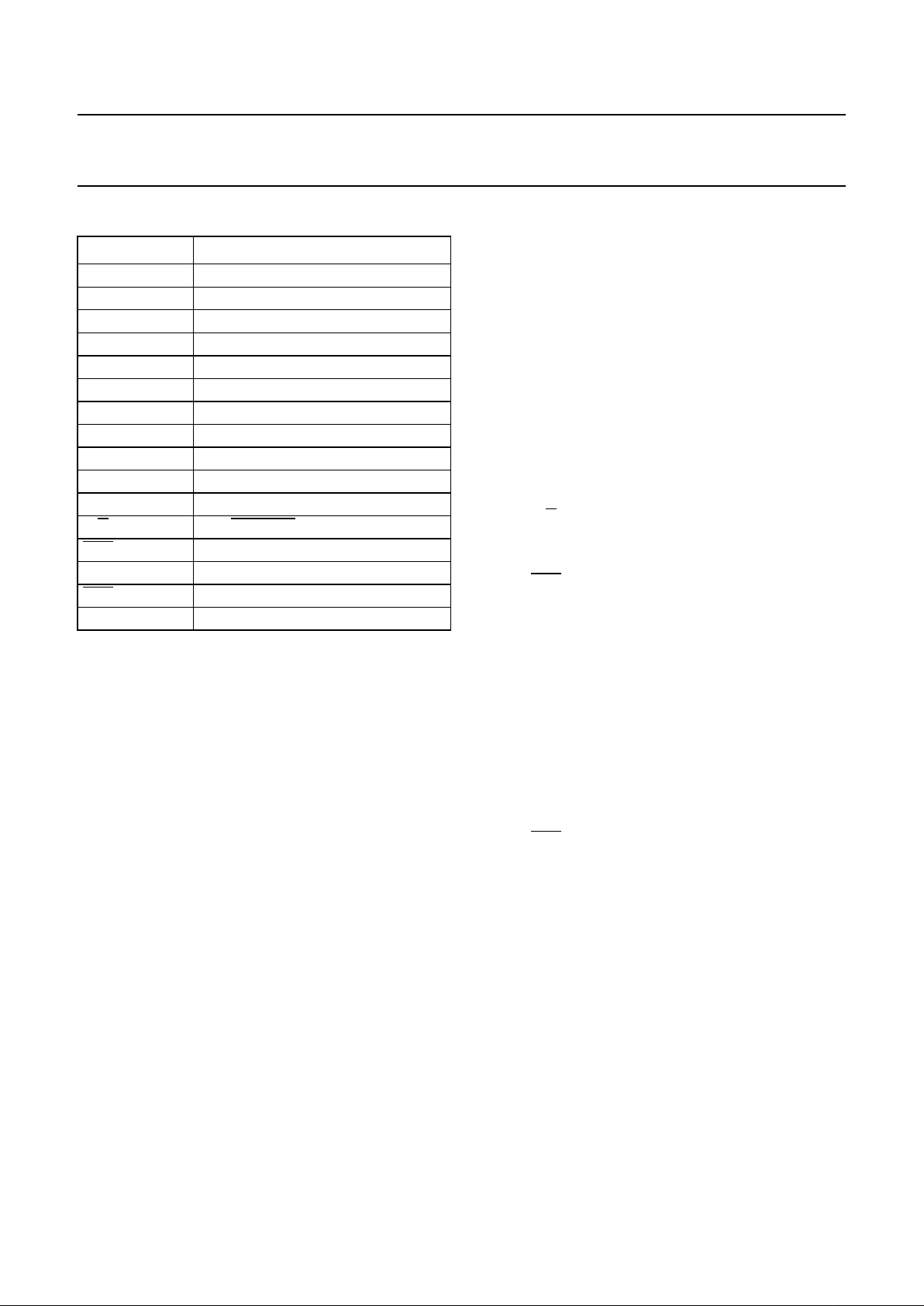
1. For further details, see Fig.18 and Table 7.
6.1 Pin functions
6.1.1 R0
TO R47 ROW DRIVER OUTPUTS
These pads output the row signals.
6.1.2 C0
TO C83 COLUMN DRIVER OUTPUTS
These pads output the column signals.
6.1.3 V
SS1,VSS2
: NEGATIVE POWER SUPPLY RAILS
Supply rails V
SS1
and V
SS2
must be connected together.
6.1.4 V
DD1,VDD2
: POSITIVE POWER SUPPLY RAILS
Supply rails V
DD1
and V
DD2
must be connected together.
SYMBOL DESCRIPTION
R0 to R47 LCD row driver outputs
C0 to C83 LCD column driver outputs
V
SS1,VSS2
ground
V
DD1,VDD2
supply voltage
V
LCD1,VLCD2
LCD supply voltage
T1 test 1 input
T2 test 2 output
T3 test 3 input/output
T4 test 4 input
SDIN serial data input
SCLK serial clock input
D/
C data/command
SCE chip enable
OSC oscillator
RES external reset input
dummy1, 2, 3, 4 not connected
6.1.5 V
LCD1,VLCD2
: LCD POWER SUPPLY
Positive power supply for the liquid crystal display. Supply
rails V
LCD1
and V
LCD2
must be connected together.
6.1.6 T1, T2, T3
AND T4: TEST PADS
T1, T3 and T4 must be connected to VSS, T2 is to be left
open. Not accessible to user.
6.1.7 SDIN:
SERIAL DATA LINE
Input for the data line.
6.1.8 SCLK:
SERIAL CLOCK LINE
Input for the clock signal: 0.0 to 4.0 Mbits/s.
6.1.9 D/
C: MODE SELECT
Input to select either command/address or data input.
6.1.10
SCE: CHIP ENABLE
The enable pin allows data to be clocked in. The signal is
active LOW.
6.1.11 OSC:
OSCILLATOR
When the on-chip oscillator is used, this input must be
connected to VDD. An external clock signal, if used, is
connected to this input. If the oscillator and external clock
are both inhibited by connecting the OSC pin to VSS, the
display is not clocked and may be left in a DC state.
To avoid this, the chip should always be put into
Power-down mode before stopping the clock.
6.1.12
RES: RESET
This signal will reset the device and must be applied to
properly initialize the chip. The signal is active LOW.

1999 Apr 12 6
Philips Semiconductors Product specification
48 × 84 pixels matrix LCD controller/driver PCD8544
7 FUNCTIONAL DESCRIPTION
7.1 Oscillator
The on-chip oscillator provides the clock signal for the
display system. No external components are required and
the OSC input must be connected to V
DD
. An external
clock signal, if used, is connected to this input.
7.2 Address Counter (AC)
The address counter assigns addresses to the display
data RAM for writing. The X-address X
6
to X0 and the
Y-address Y2to Y0 are set separately. After a write
operation, the address counter is automatically
incremented by 1, according to the V flag.
7.3 Display Data RAM (DDRAM)
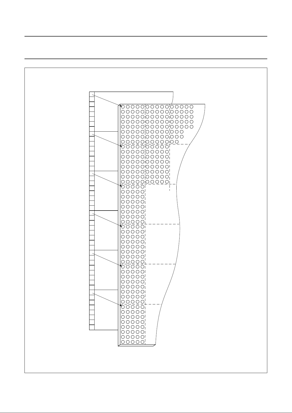
The DDRAM is a 48 × 84 bit static RAM which stores the
display data. The RAM is divided into six banks of 84 bytes
(6 × 8 × 84 bits). During RAM access, data is transferred
to the RAM through the serial interface. There is a direct
correspondence between the X-address and the column
output number.
7.4 Timing generator
The timing generator produces the various signals
required to drive the internal circuits. Internal chip
operation is not affected by operations on the data buses.
7.5 Display address counter
The display is generated by continuously shifting rows of
RAM data to the dot matrix LCD through the column
outputs. The display status (all dots on/off and
normal/inverse video) is set by bits E and D in the ‘display
control’ command.
7.6 LCD row and column drivers
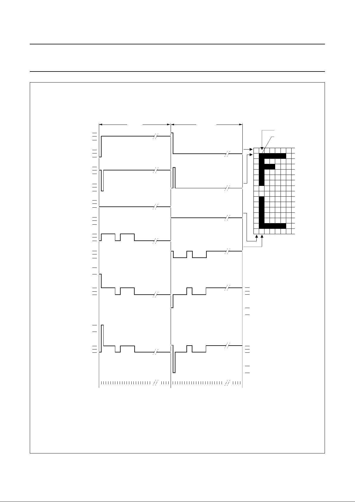
The PCD8544 contains 48 row and 84 column drivers,
which connect the appropriate LCD bias voltages in
sequence to the display in accordance with the data to be
displayed. Figure 2 shows typical waveforms. Unused
outputs should be left unconnected.

1999 Apr 12 7
Philips Semiconductors Product specification
48 × 84 pixels matrix LCD controller/driver PCD8544
Fig.2 Typical LCD driver waveforms.
V
state1
(t) =C1(t) - R0(t).
V
state2
(t) = C1(t) - R1(t).
MGL637
ROW 0
R0 (t)
ROW 1
R1 (t)
COL 0
C0 (t)
COL 1
C1 (t)
V
LCD
V
2
V
3
V
4
V
5
V
SS
V
LCD
V
SS
V
LCD
V
SS
V
LCD
V
LCD
V3 - V
SS
V
LCD
- V
2
V3 - V
2
0 V
V
LCD
V3 - V
SS
V
LCD
- V
2
V3 - V
2
0 V
−V
LCD
V4 - V
LCD
V
SS
- V
5
V4 - V
5
0 V
−V
LCD
V4 - V
LCD
V
SS
- V
5
V4 - V
5
0 V
V
SS
V
2
V
3
V
4
V
5
V
2
V
3
V
4
V
5
V
2
V
3
V
4
V
5
frame n frame n + 1
012345678 012345678
... 47 ... 47
V
state1
(t)
V
state2
(t)
V
state1
(t)
V
state2
(t)

1999 Apr 12 8
Philips Semiconductors Product specification
48 × 84 pixels matrix LCD controller/driver PCD8544
Fig.3 DDRAM to display mapping.
top of LCD
MGL636
DDRAM
bank 0
R0
R8
R16
R24
R32
R40
R47
bank 1
bank 2
bank 3
bank 4
bank 5
LCD

1999 Apr 12 9
Philips Semiconductors Product specification
48 × 84 pixels matrix LCD controller/driver PCD8544
7.7 Addressing
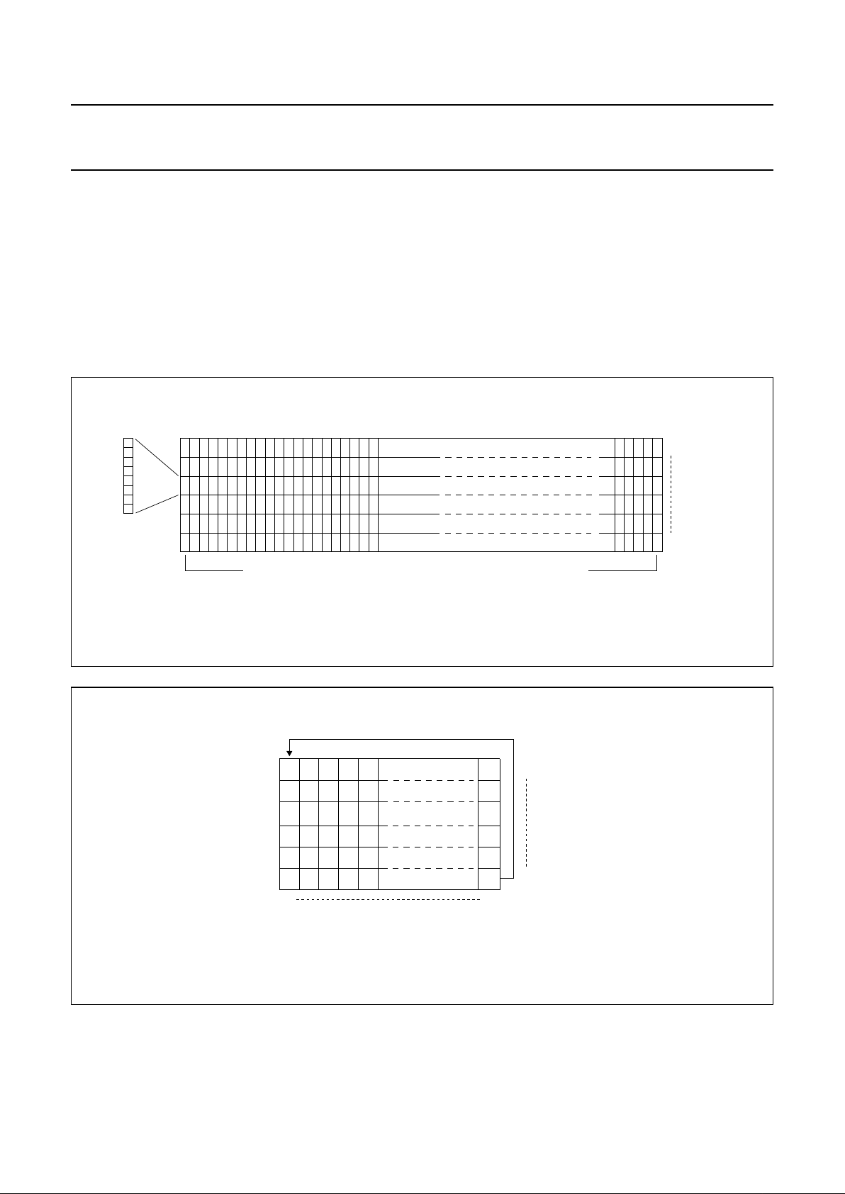
Data is downloaded in bytes into the 48 by 84 bits RAM
data display matrix of PCD8544, as indicated in
Figs. 3, 4, 5 and 6. The columns are addressed by the
address pointer. The address ranges are: X 0 to 83
(1010011), Y 0 to 5 (101). Addresses outside these
ranges are not allowed. In the vertical addressing mode
(V = 1), the Y address increments after each byte (see
Fig.5). After the last Y address (Y = 5), Y wraps around
to 0 and X increments to address the next column. In the
horizontal addressing mode (V = 0), the X address
increments after each byte (see Fig.6). After the last
X address (X = 83), X wraps around to 0 and
Y increments to address the next row. After the very last
address (X = 83 and Y = 5), the address pointers wrap
around to address (X=0andY=0).
7.7.1 D
ATA STRUCTURE
Fig.4 RAM format, addressing.
handbook, full pagewidth
MGL638
0
0
5
LSB
MSB
Y-address
X-address
83
Fig.5 Sequence of writing data bytes into RAM with vertical addressing (V = 1).
handbook, halfpage
MGL639
0
0
55035
4
3
2
107
6
Y-address
X-address
83

1999 Apr 12 10
Philips Semiconductors Product specification
48 × 84 pixels matrix LCD controller/driver PCD8544
Fig.6 Sequence of writing data bytes into RAM with horizontal addressing (V = 0).
handbook, halfpage
MGL640
0
0
5503420
336
252
168
421
337
253
169
84085
1
422
338
254
170
86
2
Y-address
X-address
83
7.8 Temperature compensation
Due to the temperature dependency of the liquid crystals’
viscosity, the LCD controlling voltage V
LCD
must be
increased at lower temperatures to maintain optimum
contrast. Figure 7 shows V
LCD
for high multiplex rates.
In the PCD8544, the temperature coefficient of V
LCD
, can
be selected from four values (see Table 2) by setting bits
TC1and TC0.
Fig.7 V
LCD
as function of liquid crystal temperature (typical values).
handbook, halfpage
MGL641
0 °C
(1)
(2)
(3)
(4)
V
LCD
temperature
(1) Upper limit.
(2) Typical curve.
(3) Temperature coefficient of IC.
(4) Lower limit.
 Loading...