

Philips PCD6001H, PCD6001U Datasheet
INTEGRATED CIRCUITS
DATA SH EET
PCD6001
Digital telephone answering
machine chip
Product specification
Supersedes data of 2001 Feb 05
File under Integrated Circuits, IC17
2001 Apr 17

Philips Semiconductors Product specification
Digital telephone answering machine chip PCD6001
CONTENTS
1 FEATURES
2 APPLICATION SUMMARY
2.1 Metalink emulation
3 GENERAL DESCRIPTION
4 ORDERING INFORMATION
5 BLOCK DIAGRAM
6 PINNING INFORMATION
6.1 Pinning
6.2 Pin description
6.3 Pin types
7 FUNCTIONAL DESCRIPTION
7.1 Architecture
7.2 I/O summary
7.3 Overview of functional description
8 POWER SUPPLY, RESET AND START-UP
8.1 Power supply
8.2 Reset and start-up
9 TICB - GENERATION AND SELECTION OF
SYSTEM CLOCKS
9.1 Microprocessor, DSP, CODEC and IOM clock
generation
9.2 System clocks
9.3 Real-Time Clock generation
10 THE MICROCONTROLLER
10.1 Microcontroller architecture
10.2 Memory mapping
10.3 SFR mapping
10.4 Microcontroller interrupts
10.5 Interface to DSP
10.6 Interface to Real-Time Clock (RTC)
10.7 Interface to the Memory Control Block (MCB)
10.8 The test registers CDTRx, PMTRx and TCTRL
10.9 Interface to Timing and Control Block (TICB)
10.10 Power and Interrupt Control Register (PCON)
10.11 I2C-bus
10.12 MSK modem
10.13 LE control
11 DSP I/O REGISTERS
11.1 Interface to CODEC
12 EXTERNAL MEMORY INTERFACE
12.1 Supported flash memories
12.2 DTAM external interface during target
debugging
13 THE CODECs
13.1 Definitions
13.2 CODEC architecture
14 ANALOG VOLTAGE REFERENCE (AVR)
14.1 Bandgap reference
14.2 Analog Voltage Source (AVS)
15 IOM
15.1 Features
15.2 Pin description
15.3 Functional description
15.4 IOM data buffers
15.5 IOM Control Register (IOMC)
15.6 Timing
16 EXTERNAL I/O INTERFACES
16.1 External analog interfaces
16.2 External digital Interfaces
17 ELECTRICAL CHARACTERISTICS
17.1 Limiting values
17.2 Supply characteristics
17.3 Digital I/O
17.4 Analogsuppliesandgeneral purposeADC and
DAC
17.5 CODECs
18 APPLICATION DIAGRAMS
19 PACKAGE OUTLINE
20 SOLDERING
20.1 Introduction to soldering surface mount
packages
20.2 Reflow soldering
20.3 Wave soldering
20.4 Manual soldering
20.5 Suitability of surface mount IC packages for
wave and reflow soldering methods
21 DATA SHEET STATUS
22 DEFINITIONS
23 DISCLAIMERS
24 PURCHASE OF PHILIPS I2C COMPONENTS
2001 Apr 17 2

Philips Semiconductors Product specification
Digital telephone answering machine chip PCD6001
1 FEATURES
• Excellent speech quality at average:
2.6, 3.2 or 5.2 kbits/s compression rate
• Excellent background noise suppression for speech
quality improvement
• Speech compression rate selection: 2.6, 3.2 or
5.2 kbits/s
• Speech decompression rate selection: 2.6, 3.2 or
5.2 kbits/s
• Variable playback speed: 50%,100% and 200% of real
time
• Voice prompt playback
• Philips International Language Library (PILL) support
tools available; coding at 2.6, 3.2 or 5.2 kbits/s
• Voice operated start message recording (VOX)
• Call progress detection by busy tone detection and
programmable silence detection
• Recording time of minimum 20 minutes in 4-Mbit flash
memory (at 3.2 kbits/s)
• Excellent true full-duplex handsfree performance
provided by Philips ‘phlux’ algorithm
• On-hook caller ID detection according to Bell 202 and
V.23 standards, as well as DTMF caller ID support
• Caller Alerting Signal (CAS) - caller ID level 2
• Dual tone generation for DTMF, melody tones and
information tones
• Optional dial tone detection, and optional ringing
detection using hardware Caller Identification (CID)
interface
• DTMF detection (for remote control function) with local
echo canceller for high reliability
• Digital volume control
• Mixeddigital/analog adaptivelimitand/orlevelcontrolof
audio input signals
• Programmable analog CODEC gainfor easy interfacing
• Internal 80C51 microcontroller can operate as system
controller; with selectable operating frequencies
between 1 and 21 MHz
• Internal 80C51 microcontroller emergency operation
down to2.2 V eliminatesthe needfor externaldiallersin
telephone answering machine applications
• Standard 80C51 developmenttools allow fast design of
Man-Machine-Interface (MMI) features
• On-board Minimum Shift Keying (MSK) modem for
CT0/CT1 applications
• Two integrated differential bit stream Analog-to-Digital
Converters (ADCs) for high quality audio input
• Two integrated differential bitstream Digital-to-Analog
Converters (DACs) for high quality audio output
• Software selectable auxiliary CODEC input channel
• Up to 38 generalpurpose digital I/O lines (mostof them
bidirectional) includingI2C-bus, availablefor connection
to keyboard, display, line interface, etc.
• On-chip 2-channel time multiplexed 8-bit general
purpose ADC for e.g. parallel set detection and battery
voltage measurement
• On-chip 8-bit general purpose DAC for e.g. speaker
amplifier volume control
• Day and time stamp possibility using built-in Real-Time
Clock
• Flexible speech memory interface for connection of
several types of speech flash memory (serial, CAD or
parallel) and DRAM
• I2C master/slave bus for peripheral control or I2C-bus
speech memory access
• Extensive power management support for battery and
emergency operation, also allowing portable (voice
memo) applications
• Digital IOM A/u-law interface for Slave or Master mode
operation at various bit rates
• Emergency operation from telephone line power only;
microprocessor and DTMF generator continue to
operate in this mode
• On-chip software switchable supply voltage for electret
microphone
• Single low supply voltage (2.2 to 2.8 V)
• Built-in single low-frequency, low-power, crystal or
ceramic resonator oscillator and on-chip PLL to reduce
EMI
• Stand-alone operation with low cost PAL, NTSC and
DTMF crystals
• API providing flash memory management functions
such as speech, telephone or CID data storage
• Pin and software compatible with the PCD6002
OTP-device (see Application note for restrictions).
2001 Apr 17 3

Philips Semiconductors Product specification
Digital telephone answering machine chip PCD6001
2 APPLICATION SUMMARY
The PCD6001 can be used in various applications, some
of which are listed below. Refer to Chapter 18 for the
corresponding outline application diagrams.
• Stand-alone digital answering machine; with handsfree
• Feature phone with integrated digital answering
machine and full-duplex handsfree
• Dual-line digital answering machines
• Analog cordless applications such as CT0/1 base
stations; with handsfree and MSK modem function for
RF digital data transmission
• Portable voice memo recorders
• Automotive applications- carstatus announcements for
example
• Low-cost desktop video conferencing
• IOM master/slave interface to connect directly to digital
systems like ISDN and DECT.
2.1 Metalink emulation
Metalink emulation is supported with the standard
package.
3 GENERAL DESCRIPTION
The PCD6001integrates all the digitaland analog speech
management and processing functions required for a
feature-phone with integrated digital answering machine,
or a stand-alone digital answering machine into a single
low-cost chip.
Key hardware features which give the chip distinct
advantages in performance and application over
competitive solutions include:
• The flexibility to change the MMI
• An easy-to-program standard 80C51 microcontroller
with 32-kbyte internal ROM memory
• High 80C51microprocessor powerfor systemcontroller
functions of CT0/CT1 system control functions
• Up to 38 generalpurpose I/O lines for peripheral control
• I2C-bus interface
• Flexible flash memory control to interface to several
types of serial and parallel flash memory
• Two integrated 16-bit bitstream audioCODECs for true
full-duplex handsfreeoperation or dual-line stand-alone
answering machine operation
• Internal Digital Speech Processor (DSP) for excellent
‘HARMONY’ sinusoidal speech compression,
decompression and variable playback speed
• Embedded DTMF detection, call progress detection,
voice operated recording (VOX)
• High quality caller ID FSK demodulation and Caller
Alerting Signal (CAS) detection for CID level 2
• Two channel telephone line input for caller ID FSK and
audio interfacing.
Philips provides a sophisticated API running on the
internal 80C51, allowing product developers to design
their MMIs quickly to suit particular applications. The API
takes care of all flash memory and DSP management
tasks and can be enhanced on request.
For the pre-recorded voice prompts, the Philips
International Language Library (PILL) tools are available
for astandard multimediaPC platform underWindows 95.
These tools provide a way to compile a range of
multi-lingual voice prompts for efficient storage in the
speech (flash) memory. The PILL tools support various
languages and their grammar adaptations.
4 ORDERING INFORMATION
TYPE
NUMBER
PCD6001H QFP80 plastic quadflat package;80 leads (leadlength 1.95 mm);
PCD6001U U/10 sawn wafer on Film Frame Carrier (delivery as Known
2001 Apr 17 4
NAME DESCRIPTION VERSION
body 14 × 20 × 2.8 mm
Good Dies)
PACKAGE
TEMPERATURE
RANGE (°C)
SOT318-2 −25 to +70
−−25 to +70

Philips Semiconductors Product specification
Digital telephone answering machine chip PCD6001
5 BLOCK DIAGRAM
handbook, full pagewidth
V
DDA
V
SSA
XTAL2
XTAL1
V
BGP
V
REF
V
MIC
AD1IN
AD0IN
DAOUT
LIFMOUT
LIFPOUT
LIFPIN
LIFMIN1
LIFMIN2
SPKRP
SPKRM
MICP
MICM
V
34
28
41
42
29
30
27
32
31
33
38
39
35
37
36
23
24
25
26
V
DDPLL
SSPLL
43 40 53 12 44
WAKE-UP
RSTANA
OSCILLATOR
and PLL
ANALOG
VOLTAGE
REFERENCE
and SUPPLY
GENERAL
PURPOSE
A/D and D/A
CODEC 1
(ANALOG)
CODEC 2
(ANALOG)
V
DD3V1
MICROCONTROLLER
events
CLK
TICB
PCD6001
CODEC 1
(DIGITAL)
CODEC 2
(DIGITAL)
V
µC_CLK
wake-up
DSPCLK
DD3V2
80C51
idle
V
DD3V3
DMI
DSP
plus
ROM,
RAM
MAIN and
AUX RAM
WATCHDOG
V
SS3V1
13 61 22
ALE, RDN, WRN
PSEN
P4.3
P0
MA
P2
main bus
MCB
I2C-
BUS
MSKIOM
V
SS3V2
32 KBYTE
ROM
AND
EXTERNAL
INTERFACE
P4
P1
V
SS3V3
11 to 4
80 to 73
72 to 65
14 to 18
54
55
3
2
62
1
64
63
56
57
58
59
60
19
20
21
TST
RSTIN
ALE
EA
MA7 to MA0
P2.7 to P2.0
P0.7 to P0.0
P4.3
PSEN
WR
RD
P4.0/LE
P4.1/FSK
P4.2/FSO
P4.4/FSI
P4.5/GPC
P1.0/EX2 to
P1.4/EX6
P1.5
P1.6/SCL
P1.7/SDA
46
45
P3.1/
MOUT1/
DCK
P3.0/
MOUT0/
DO
Fig.1 Block diagram.
2001 Apr 17 5
P3.2/
EX0N
47
P3.3/
EX1N
P3
52
51
50
49
48
MGT427
P3.5/
T1
P3.4/
T0
P3.7/
MIN/
DI
P3.6/
MOUT2/
FSC

Philips Semiconductors Product specification
Digital telephone answering machine chip PCD6001
6 PINNING INFORMATION
6.1 Pinning
handbook, full pagewidth
PSEN
EA
ALE
MA0
MA1
MA2
MA3
MA4
MA5
MA6
MA7
V
DD3V2
V
SS3V1
P1.0/EX2
P1.1/EX3
P1.2/EX4
P1.3/EX5
P1.4/EX6
P1.5
P1.6/SCL
P1.7/SDA
V
SS3V3
SPKRP
SPKRM
P2.4
P2.3
P2.2
P2.1
P2.0
P0.7
P0.6
P0.5
P0.4
P0.3
P0.2
P0.1
P2.7
P2.6
P2.5
80
79
78
77
76
75
74
73
1
2
3
4
5
6
7
8
9
10
11
12
13
14
15
16
17
18
19
20
21
22
23
24
PCD6001
71
72
70
69
68
67
P0.0
66
65
WR
64
RD
63
P4.3
62
V
61
SS3V2
P4.5/GPC
60
P4.4/FSI
59
P4.2/FSO
58
P4.1/FSK
57
P4.0/LE
56
RSTIN
55
TST
54
V
53
DD3V1
P3.7/MIN/DI
52
P3.6/MOUT2/FSC
51
P3.5/T1
50
P3.4/T0
49
P3.3/EX1N
48
P3.2/EX0N
47
P3.1/MOUT1/DCK
46
P3.0/MOUT0/DO
45
V
44
DD3V3
V
43
DDPLL
XTAL1
42
XTAL2
41
25
26
27
28
29
30
31
32
MICP
MICM
MIC
V
SSA
V
BGP
V
REF
V
AD0IN
AD1IN
Fig.2 Pin configuration.
2001 Apr 17 6
33
V
DAOUT
34
DDA
35
LIFPIN
36
37
LIFMIN2
LIFMIN1
38
39
LIFPOUT
LIFMOUT
40
SSPLL
V
MGT428

Philips Semiconductors Product specification
Digital telephone answering machine chip PCD6001
6.2 Pin description Table 1 QFP80 package
SYMBOL PIN I/O
RESET
STATE
PIN TYPE
(1)
DESCRIPTION
PSEN 1 O H ucp4mthuwh program store enable (80C51)
EA 2 I Z ucp4mthuwh external access NOT (80C51)
ALE 3 O H ucp4mthuwh address latch enable signal (80C51)
MA0 4 O L ops10c general purpose output;
MA1 5 O L ops10c general purpose output;
MA2 6 O L ops10c general purpose output;
MA3 7 O L ops10c general purpose output;
MA4 8 O L ops10c general purpose output;
MA5 9 O L ops10c general purpose output;
MA6 10 O L ops10c general purpose output;
MA7 11 O L ops10c general purpose output;
V
DD3V2
V
SS3V1
12 power supply positive supply 2 (3.0 V) for digital circuitry
13 power supply ground supply 1 for digital circuitry
EA = 1; add_low; EA = 0
EA = 1; add_low; EA = 0
EA = 1; add_low; EA = 0
EA = 1; add_low; EA = 0
EA = 1; add_low; EA = 0
EA = 1; add_low; EA = 0
EA = 1; add_low; EA = 0
EA = 1; add_low; EA = 0
P1.0/EX2 14 I/O H ucp4mthuwh 80C51 port pin/EX2 input
P1.1/EX3 15 I/O H ucp4mthuwh 80C51 port pin/EX3 input
P1.2/EX4 16 I/O H ucp4mthuwh 80C51 port pin/EX4 input
P1.3/EX5 17 I/O H ucp4mthuwh 80C51 port pin/EX5 input
P1.4/EX6 18 I/O H ucp4mthuwh 80C51 port pin/EX6 input
P1.5 19 I/O H ucp4mthuwh 80C51 port pin
P1.6/SCL 20 I/O Z I
P1.7/SDA 21 I/O Z I
V
SS3V3
22 power supply ground supply 3 for digital circuitry
2
C400k 80C51 port pin/I2C-bus clock
2
C400k 80C51 port pin/I2C-bus data
SPKRP 23 O Z ana positive output to speaker from CODEC2 (handsfree)
SPKRM 24 O Z ana negative output to speaker from CODEC2 (handsfree)
MICP 25 I 0.625 V ana positive input from microphone to CODEC2 (handsfree)
MICM 26 I 0.625 V ana negative input from microphone to CODEC2 (handsfree)
V
V
V
V
MIC
SSA
BGP
REF
27 O Z ana positive microphone supply voltage (2 V)
28 power supply ground supply voltage for analog circuits
29 O 1.25 V band gap output voltage (V
30 O 2.00 V ana reference voltage (V
REF
)
BGP
)
AD0IN 31 I − ana analog input channel 1 for general purpose ADC
AD1IN 32 I − ana analog input channel 2 for general purpose ADC
DAOUT 33 O 0.5V
V
DDA
34 power supply positive supply (2.5 V) for analog circuits
ana analog output channel for general purpose D/A converter
DDA
LIFPIN 35 I 0.625 V ana positive analog input of CODEC1 (line CODEC)
LIFMIN2 36 I 0.625 V ana negative analog input 2 of CODEC1 (line CODEC)
LIFMIN1 37 I 0.625 V ana negative analog input 1 of CODEC1 (line CODEC)
LIFMOUT 38 O Z ana negative analog output of CODEC1 (line CODEC)
2001 Apr 17 7
Philips Semiconductors Product specification
Digital telephone answering machine chip PCD6001
SYMBOL PIN I/O
RESET
STATE
PIN TYPE
(1)
DESCRIPTION
LIFPOUT 39 O Z ana positive analog output of CODEC1 (line CODEC)
V
SSPLL
40 power supply ground supply for XTAL clock and PLL circuitry
XTAL2 41 O running ana crystal oscillator output
XTAL1 42 I − ana crystal oscillator input
V
DDPLL
V
DD3V3
43 power supply positive supply (2.5 V) for XTAL clock and PLL circuitry
44 power supply positive supply 3 (3.0 V) for digital circuitry
P3.0/MOUT0/DO 45 I/O H ucp4mthuwh 80C51 port pin/MSK output 0/IOM data output
P3.1/MOUT/DCK 46 I/O H ucp4mthuwh 80C51 port pin/MSK output 1/IOM DCK signal
P3.2/EX0N 47 I/O H ucp4mthuwh 80C51 port pin/EX0N input
P3.3/EX1N 48 I/O H ucp4mthuwh 80C51 port pin/EX1N input
P3.4/T0 49 I/O H ucp4mthuwh 80C51 port pin/Timer 0 input
P3.5/T1 50 I/O H ucp4mthuwh 80C51 port pin/Timer 1 input
P3.6/MOUT2/FSC 51 I/O H ucp4mthuwh 80C51 port pin/MSK output 2/IOM FSC signal
P3.7/MIN/DI 52 I/O H ucp4mthuwh 80C51 port pin/MSK input/IOM data input
V
DD3V1
53 power supply positive supply 1 (2.5 V) for digital circuitry
TST 54 I − iptd test input (recommended to be connected to ground)
RSTIN 55 I − ipth reset in
P4.0/LE 56 I/O L ucp4mthuwh general purpose I/O/LCD enable, configured as ODafter
reset
P4.1/FSK 57 I/O Z ucp4mthuwh general purpose I/O/Flash Serial Clock, configured
as OD after reset
P4.2/FSO 58 I/O Z ucp4mthuwh general purpose I/O/Flash Serial Out, configured as OD
after reset
P4.4/FSI 59 I/O Z ucp4mthuwh general purpose I/O/Flash Serial In, configured as OD
after reset
P4.5/GPC 60 I/O L ucp4mthuwh general purpose I/O/GP clock output (crystal clock or
microcontroller clock), configured as OD after reset
V
SS3V2
61 power supply negative supply 2 (ground) for digital circuitry
P4.3 62 I/O Z ucp4mthuwh general purpose I/O, configured as OD after reset
RD 63 O Z ucp4mthuwh 80C51 read NOT, configured as OD after reset
WR 64 O Z ucp4mthuwh 80C51 write NOT, configured as OD after reset
P0.0 65 I/O Z uceda4mtuwh 80C51 Port 0 input/output
P0.1 66 I/O Z uceda4mtuwh 80C51 Port 0 input/output
P0.2 67 I/O Z uceda4mtuwh 80C51 Port 0 input/output
P0.3 68 I/O Z uceda4mtuwh 80C51 Port 0 input/output
P0.4 69 I/O Z uceda4mtuwh 80C51 Port 0 input/output
P0.5 70 I/O Z uceda4mtuwh 80C51 Port 0 input/output
P0.6 71 I/O Z uceda4mtuwh 80C51 Port 0 input/output
P0.7 72 I/O Z uceda4mtuwh 80C51 Port 0 input/output
P2.0 73 O L ucp4mthuwh general purpose output,
P2.1 74 O L ucp4mthuwh general purpose output,
EA = 1; add_high; EA = 0
EA = 1; add_high; EA = 0
2001 Apr 17 8
Philips Semiconductors Product specification
Digital telephone answering machine chip PCD6001
SYMBOL PIN I/O
RESET
STATE
PIN TYPE
(1)
P2.2 75 O L ucp4mthuwh general purpose output,
P2.3 76 O L ucp4mthuwh general purpose output,
P2.4 77 O L ucp4mthuwh general purpose output,
P2.5 78 O L ucp4mthuwh general purpose output,
P2.6 79 O L ucp4mthuwh general purpose output,
P2.7 80 O L ucp4mthuwh general purpose output,
Note
1. The pin type codes are explained in Section 6.3.
6.3 Pin types
6.3.1 POWER SUPPLY PINS
There are 6 different power supply domains (see Fig.3):
• Digital core circuit (2.5 V): V
• Digital periphery circuit (3.0 V): V
V
DD3V3/VSS3V3
• PLL circuits and crystal oscillator (2.5 V): V
V
SSPLL
• Analog circuits (2.5 V): V
DD3V1/VSS3V1
and V
DDA
DD3V2/VSS3V2
DDPLL
.
SSA
and
and
All VSSpins must beconnected to the same ground plane
on the Printed-Circuit Board (PCB). All 2.5 V VDD pins
must beconnected tothe samepower supply.All VDDpins
have tobe separatelydecoupled, accordingto Chapter 18.
6.3.2 ANALOG PINS
• ana: full ESD protected analog I/O pad (double
protection diode).
6.3.3 DIGITAL PINS
• ucp4mthuwh: 4 mA 80C51 I/O pins
• uceda4mtuwh: 4 mA 80C51 I/O pins with input enable
• iptd: input pad buffer; pull-down
• ipth: input pad buffer with Schmitt trigger
• ops10c: outputpad; push-pull; 4 mA outputdrive; 10 ns
slew control
• I2C400k: bidirectional open-drain I2C-bus compatible
pad.
DESCRIPTION
EA = 1; add_high; EA = 0
EA = 1; add_high; EA = 0
EA = 1; add_high; EA = 0
EA = 1; add_high; EA = 0
EA = 1; add_high; EA = 0
EA = 1; add_high; EA = 0
V
handbook, halfpage
DD3V1
V
SS3V1
V
DD3V2
V
SS3V2
V
DD3V3
V
SS3V3
Fig.3 PCD6001 chip supply rails with protection diodes.
2001 Apr 17 9
V
DDPLL
V
SSPLL
V
DDA
V
SSA
MGT429

Philips Semiconductors Product specification
Digital telephone answering machine chip PCD6001
7 FUNCTIONAL DESCRIPTION
7.1 Architecture
ThePCD6001architecture isbased onan embedded8-bit
80C51 microcontroller, a Philips ‘REAL’ DSP core, two
high quality AD/DA CODECs and a 32-kbyte ROM
microcontroller memory. Refer to the block diagram in
Chapter 5.
The most important DSP peripherals are the:
• CODECs
• DSP program ROM
• DSP RAM
• IOM interface.
The most important microcontroller peripherals are the:
• Memory Control Block (MCB)
• Watchdog Timer
• General purpose ports
• I2C-bus interface
• MSK block (used for digital data transfer and analogue
cordless applications).
The MCB, through Ports P0, P2, P4 and Memory
Address (MA) can interface to various types of flash
memory including serial, parallel or multiplexed
command/address/data. Most of the peripherals are
controlled via microcontroller special function registers.
The microcontroller initializes and controls the:
• DSP via the DSP to Microcontroller Interface (DMI)
• Speech flash memory via the Memory Control
Block (MCB), and P0/P4 port pins
• Clock and power settings via the Timing and Control
Block (TICB)
• Analog sectionvia its SpecialFunction Registers (SFR).
7.2 I/O summary
All digital I/O for peripherals such as keyboard, display,
line interface and others are handled by the
microcontroller via ports P0, P1, P2, P3, P4, and MA.
Port 2 and MA provide 16 general purpose output-only
lines (not bit-addressable, push-pull, 4 mA) to drive
peripherals.These portscan beused forperipheralcontrol
if EAis logic 1. The4 mA drivinglevel should beadequate
to drive a low power LED directly if required.
In addition to these 16 output-only lines, 16 general
purpose I/O lines are provided by Ports 1 and 3. Port 1
can handle 5 external interrupts (P1.0 to P1.4) that are
also HIGH/LOWinterrupt level programmable. Port 1also
contains the I2C-bus. Port 3 can handle an additional
2 external interrupts (P3.2 and P3.3) which are active
LOW only. The Timer 0 and Timer 1 inputs are available
on Port 3 as for the standard 80C51. Ports 1 and 3 are
80C51 weak pull-up I/O lines with a 4 mA sink capability,
with the exception of the I2C-bus lines P1.6 and P1.7
which are open-drain. If the P3 alternate port function for
the MSK modem is chosen then the standard I/O is not
available on pins P3.0, P3.1, P3.6 and P3.7.
Port 4 lines are 6 more general purpose I/O. They will be
configured as open-drain after reset. These open-drains
can be connected via pull-up resistors to the telephone
system supply or to the mains AC supply. If a flash
memory with a different supply voltage (V
DD_FLASH
up
to 3.3 V) is connected, P4.3 can be pulled-up to this
voltage. This is required such that the Chip Enable
Not (CEN) input of a flash deviceis equal to V
DD_FLASH
to
reduce the standby power consumption. All other Port 4
pins should not be pulled up to a voltage higher than
V
DD_DTAM
.
In case a CAD flash is used, P4.4 and P4.5 are free
bit-addressable ports.
All P4 pins also can be configured to push-pull via the
register P4CFG. This brings the total of I/O lines to 38 (of
which 16 are output only).
In case an I2C-bus LCD driver is used, P4.0, at which
a Latch Enable (LE) function is provided for 68xxx family
microcontroller peripherals, is an additional free
bit-addressable open-drain I/O port.
The analog interfacing for the PCD6001 consists of the
analog audio I/O of the 2 CODECs and 2 additional
general purpose analog-to-digital inputs and a general
purpose digital-to-analog outputfor voltage measurement
and control respectively. Furthermore a stabilized
microphone supply output V
is provided which can be
MIC
switched on/off for power control.
One audio CODEC is dedicated for the PSTN line
communication (CODEC1). This line CODEC has a
differential low ohmic analog output which consists of
LIFPOUT and LIFMOUT. In case only one of the
differential outputs is used, LIFPOUT should be chosen,
since the Emergency modeDTMF signal is also available.
2001 Apr 17 10

Philips Semiconductors Product specification
Digital telephone answering machine chip PCD6001
The line CODEC has 3 inputs which are configurable as
2 single-ended inputs LIFMIN1 and LIFMIN2 that can be
selected by software control, while LIFPIN is AC coupled
to ground. It is also possible to use one of the LIFMIN
inputs (leaving theother unconnected) in conjunction with
the LIFPIN input as a differential input, in case a high
CMRR is required.
The second CODEC is dedicated for a local microphone
and loudspeaker connection (CODEC2). This handsfree
CODEC has a differential low ohmic analog output which
consists of SPKRP andSPKRM.This output can be used
either differential or single ended. The speaker output
impedance and driving level is not suitable to directly
connect a speaker. The handsfree CODEC has a
differential microphone input which consists of MICP and
MICM. This differential input features a fixed 16 dB
microphone preamplifier.
Both theline and handsfreeCODEC outputshaveon-chip
filtering for outof band signals suchthat no external filters
are required.
There are 2 × 8-bit analog-to-digital inputs AD0IN and
AD1IN for voltage measurements which can be used for
parallelset detectionalgorithms orbattery control.An 8-bit
DAC output DAOUT can provide an analog peripheral
control signal.
7.3 Overview of functional description
The detailedfunctional descriptionis divided intoseparate
chapters covering the major functional blocks, as follows:
Chapter 8 “Power supply, reset and start-up”
Chapter 9 “TICB - generation and selection of system
clocks”
Chapter 10 “The microcontroller”
Chapter 11 “DSP I/O registers”
Chapter 12 “External memory interface”
Chapter 13 “The CODECs”
Chapter 16 “External I/O interfaces”.
8 POWER SUPPLY, RESET AND START-UP
8.1 Power supply
ThePCD6001 corecircuitryis suppliedby three3 Vsupply
pairs. The crystal oscillator and PLL are supplied with a
separate pair of supply pins to provide a ‘clean’ supply
voltage required for low jitter. The following supplies exist:
V
DD3V1
V
DD3V2
V
DD3V3
V
DDA
V
DDPLL
and V
and V
and V
and V
andV
: digital core supply 1 (2.5 V)
SS3V1
: digital supply 2 (3.0 V)
SS3V2
: digital supply 3 (3.0 V)
SS3V3
: analog supply (2.5 V)
SSA
:crystalclock andPLL supply(2.5 V).
SSPLL
8.2 Reset and start-up
After applyingthe power supplyvoltage, the chipwill need
an external Power-on reset via pin RSTIN. RSTIN should
remain active (logic 1) until V
again before the power supply drops below V
and has to become active
trh
.
trl
The reset via RSTIN is one of 3 possible ways to perform
a reset. The following reset conditions exist:
• Wake-up fromsystem off (crystal isoff, but poweris on)
by an external interrupt
• RSTIN, reset in from pin RSTIN
• Watchdog Timer expires.
After a Power-on reset and after a wake-up from system
off, a counter is activated, which guarantees that the first
instruction fetch of the microcontroller is delayed by at
least 4096 clock cycles.
To reduce power consumption during reset, the following
reset strategy is used. If the DSP function is not required,
it can be switched off by the microcontroller. The DSP
reset will then bedelayed (until it is switched on again), in
order to avoid a large (reset) power consumption.
2001 Apr 17 11

Philips Semiconductors Product specification
Digital telephone answering machine chip PCD6001
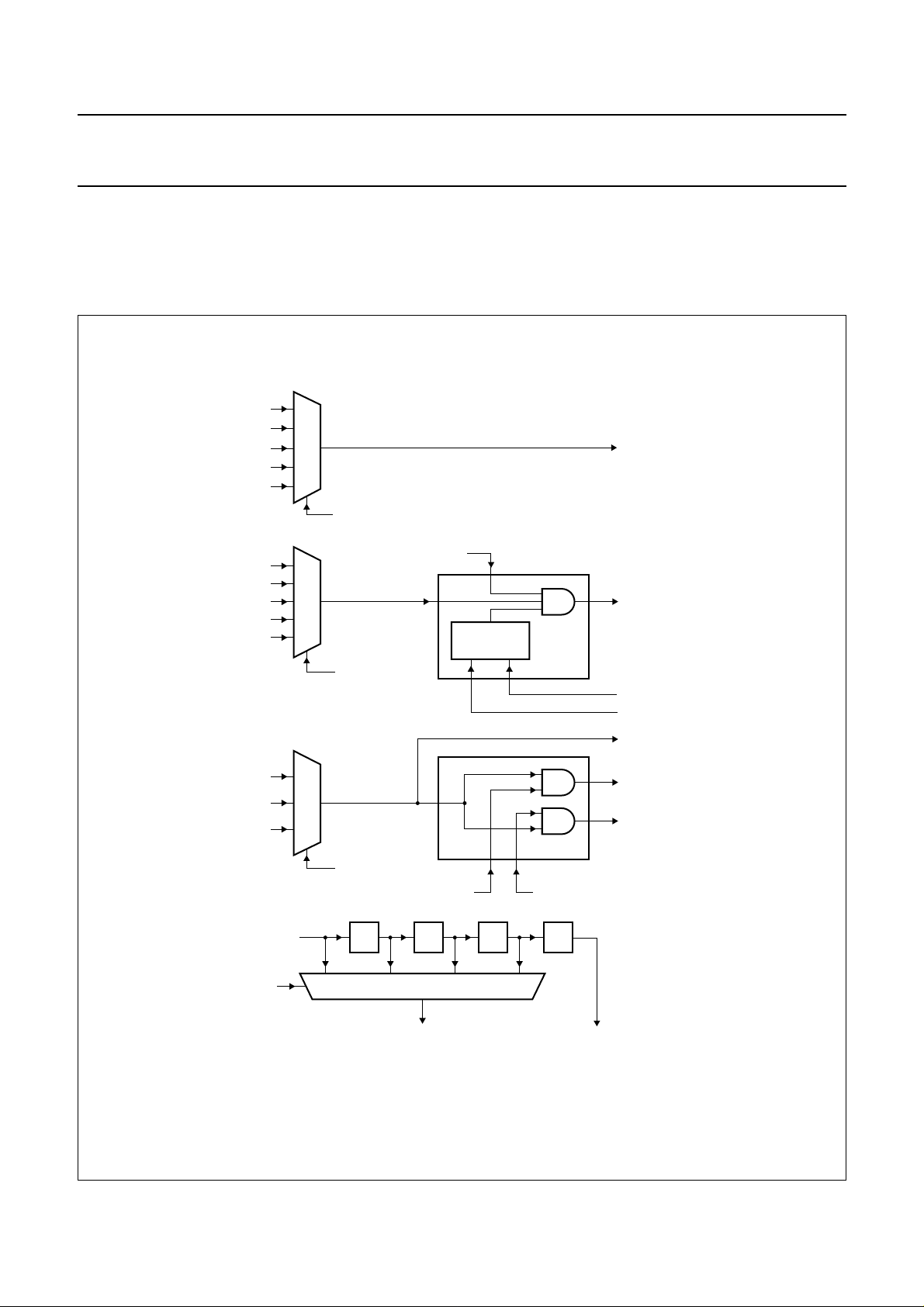
9 TICB - GENERATION AND SELECTION OF
SYSTEM CLOCKS
The TICB generates the clocks for all digital chip blocks,
and controls the on/off switching of these blocks by using
clock gating.The TICBis controlledvia themicrocontroller
SFR registers SYMOD, CKCON and SPCON. The TICB
contains:
• An input section to adapt to different input clock rates
• A clock generation section
• A clock selection section
• The Real-Time Clockfor a 1 minute interruptgeneration
• The microcontroller interrupt timers (FS_event and
TIME_event) and the DSP interrupt timer (FS1) to
respectively synchronize the microcontroller and DSP
processes.
9.1 Microprocessor, DSP, CODEC and IOM clock generation
Figure 4 shows the TICB input section and the clock
generation section.
The clock generation section contains a PLL to generate
the clock rates which are higher then the input clock rate.
With the input section, a wider variety of input clock
frequencies can be adaptedto the input frequency values
needed by the PLL (3.456 or 3.580 MHz).
In order to save power the PLL can be switched off. This
should however only be done when the chip is in the
Emergency mode. When switching on the PLL, it takes
40 µs (173 emergency clock periods) until the clock
frequencies are derived from the PLL output.
Table 2 gives a descriptionofthe signals and their values
for a crystal frequency of 3.456 and 3.580 MHz.
The clock generation section also contains logic to
synchronize the CODEC timing signals and the DSP and
microcontroller interrupt timers to an external Frame
Sync. (FSC). This synchronization is only activated when
using the IOM in Slave mode. If the IOM is activated in
Master mode, the TICB generates the DCK and
FSC signals from CLK28.
Some of the clock signals can be made available as
general purpose clock, for various peripherals needing a
clock source such as an PCA1070 line interface. This
general purpose clock (GPC) signal is an alternative
output of P4.5and can be turned on withALTP bit 3. With
ALTP bit 2, the source for GPC canbe defined. The GPC
source is EMG_CLK (normally 3.58 MHz) when bit 2 is
logic 0 andthe GPCsourceis µC_CLKwhen bit 2 isset to
logic 1. As a spike-free GPC is not guaranteed when
switching betweenthese clocks, itis recommended tofirst
set the clock source before switching on the GPC. The
ALTP register is described in more detail in Section 16.2.
2001 Apr 17 12

Philips Semiconductors Product specification
Digital telephone answering machine chip PCD6001
handbook, full pagewidth
CLK_IN
÷2
÷4
SYMOD[6 or 7]
PLL_IN
SYMOD[5
PLL_ON
on
PLL × 24
÷24
÷2
]
÷3
÷4
20.736 MHz
for a 3.456 MHz
PLL input clock
0
1
SYMOD[5
PLL_ON
CLK3_CORR
]
CLK_21
CKCON[6 or 7
CLK3_EMG
CLK3_OUT
DCK
GENERATOR
]
EMG_CLK
CLK_42
CLK_28
÷2
CLK_14
÷2
CLK_7
÷6
CLK_1
DCK
÷192
FSC
CLK_3
FS1
CLK_21 CLK_3
CLK3GEN
control and synchronization CODEC timing signals
Fig.4 TICB input section and clock generation.
2001 Apr 17 13
CDCCNTRL
MGT430
Philips Semiconductors Product specification
Digital telephone answering machine chip PCD6001
Table 2 Descriptions and frequency values for signals shown in Fig.4
SIGNAL FUNCTION
VALUE (MHz)
PLL_IN 3.456 PLL_IN 3.580
Microprocessor and DSP clock signals
EMG_CLK emergency clock 3.456 3.580
CLK_42 DSP selectable clock frequency 41.472 42.960
CLK_28 DSP selectable clock frequency 27.648 28.640
CLK_21 microcontroller selectable clock frequency 20.736 21.480
CLK_14 microcontroller selectable clock frequency 13.824 14.320
CLK_7 DSP and microcontroller selectable clock frequency 6.912 7.160
CLK_1 DSP and microcontroller selectable clock frequency 1.152 1.193
CODEC clock signals
CLK_21 input clock for phase corrected CLK3_OUT 20.736 21.480
CLK3_EMG EMG_CLK input to CLK_3 multiplexer 3.456 3.580
CLK3_CORR frequency corrected CODEC clock (24/25 × 3.58 MHz) − 3.437
CLK3_OUT phase corrected 3.456 MHz CODEC clock 3.456
(1)(2)
−
CLK14_CODEC input clock for CODECs 13.824 14.320
IOM clock/timing signals
DCKmaster the IOM master clock signal DCK generated by the TICB 1.536
FSCmaster the IOM master frame sync FSC generated by the TICB 8 kHz
(1)(3)
(1)(3)
1.527
7.955 kHz
(1)(2)
(1)(3)(4)
(1)(3)(4)
Notes
1. These values are only valid if the RTC mode bit CKCON.6 has been set according to the PLL_IN frequency used
(see also Table 6).
2. If the IOM Slave mode is activated, these clock signals are synchronized to the externally applied FSC.
3. Proper IOM functionality is only guaranteed at DSP clock frequencies of 28 and 42 MHz. If the IOM Slave mode is
activated, the externally applied DCK and FSC signals are used.
4. These master frequencies do not comply to IOM specification. For 3.58 MHz crystal operation, proper IOM
functionality is therefore only guaranteed in Master mode.
2001 Apr 17 14
Philips Semiconductors Product specification
Digital telephone answering machine chip PCD6001
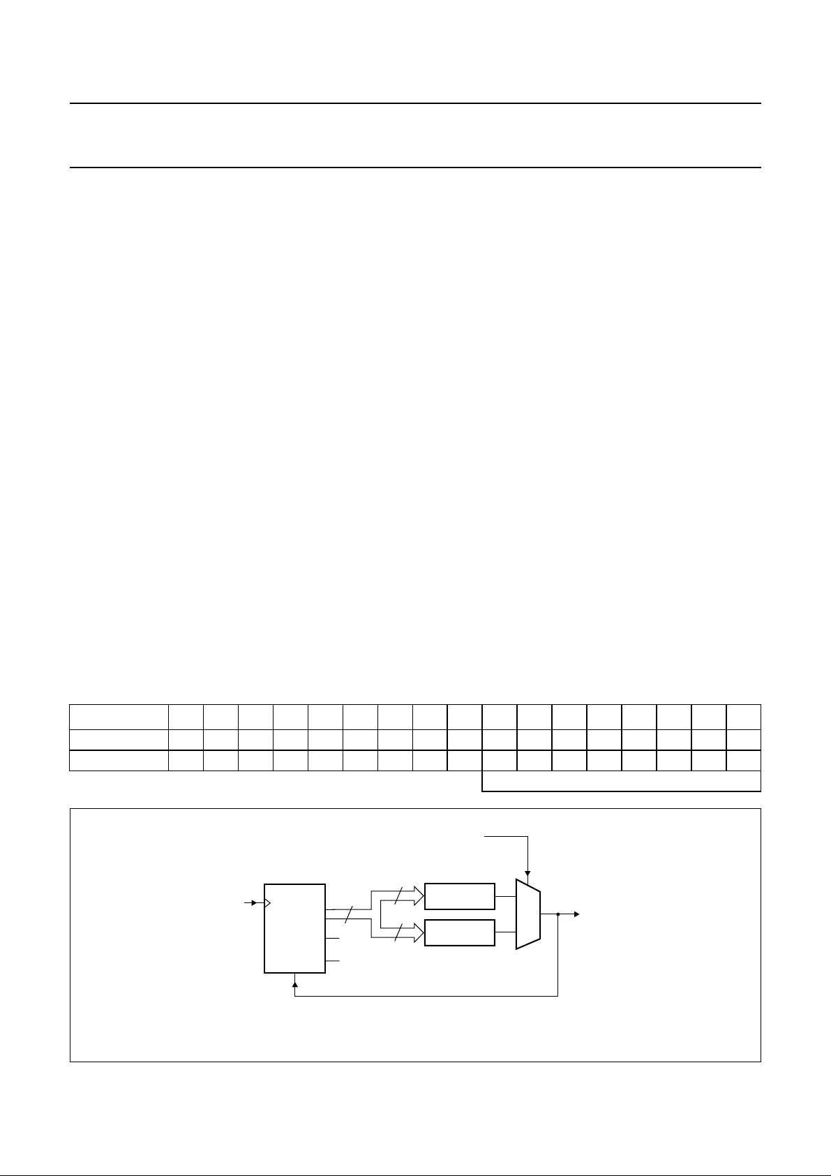
9.2 System clocks
Figure 5 shows the multiplexers with their input and control signals for the DSP processor clock, the microcontroller
clock, the CODEC clock (CLK_3) and the chip input clock frequency. The functional position of the CODEC clock
multiplexer is shown in Fig.4.
handbook, full pagewidth
EMG_CLK
CLK_1
CLK_7
CLK_14
CLK_21
EMG_CLK
CLK_1
CLK_7
CLK_42
CLK_28
EMG_CLK
CLK3_CORR
CLK3_OUT
CKCON[2, 3 or 7
SPCON[4]
DSP_CLK_IN
CKCON[4, 5 or 7
CLK_3
]
]
Q
FF
RS
µC_CLK
DSP_CLK
DSP_WAKEUP
DSP_IDLE
CDCCNTRL_CLK
CLK_3_DRT1
CLK_3_DRT2
]
SPCON[0 or 1
FS_event
CKCON[0 or 1
]
CKCON[6 or 7
FS1
÷ 4 ÷ 2 ÷ 2 ÷ 5
3210
Fig.5 Clock and event rate selection.
2001 Apr 17 15
]
SPCON[2 or 3
]
TIME_event
MGT431
Philips Semiconductors Product specification
Digital telephone answering machine chip PCD6001
9.2.1 SELECTION OF SYSTEM CLOCKS
Selection of system clocks involves:
• Selection of the crystal input clock in conjunction with
PLL on/off selection (SYMOD register)
• Selection of clocks for the DSP, microcontroller and
CODEC, together with microcontroller timing interrupt
rates (CKCON register)
• Activation, deactivation of individual clocks or
deactivation of the whole TICB in order to get an
optimum power consumption (SPCON register).
9.2.2 ANALOG SYSTEM MODE REGISTER (SYMOD)
Table 3 Analog System Mode Register (SFR address C5H); reset state 00H
7654 3 2 10
input clock 1 input clock 0 PLL off/on V
9.2.3 SYSTEM POWER AND CLOCK CONFIGURATION REGISTER (SPCON)
Table 4 System Power and Clock Configuration Register (SFR address 99H); reset state 00H
off/on CODEC2; analog CODEC1; analog
MIC
SYMOD, SPCON and CKCON are SFR registers in the
digital section which can be directly accessed by the
microcontroller. Sections 9.2.2 to 9.2.4 summarize the
control registers and settings used for system clock
selection.
The activation of the DSP, and the digital part of both
CODECs is controlled via the SPCON SFR.
The clock rates of the DSP and microcontroller, and the
microcontroller timing interrupt rates are set via the
CKCON SFR.
D/A
(loudspeaker)
off/on
A/D
(microphone)
off/on
D/A
(to_line)
off/on
A/D
(from_line)
off/on
7654 3 2 10
system off spare spare DSP on CODEC2; digital CODEC1; digital
D/A
(loudspeaker)
off/on
9.2.4 CLOCK CONTROL REGISTER (CKCON)
Table 5 Clock Control Register (SFR address 9AH); reset state 00H
76543210
EMG mode RTC mode DSP clock 1 DSP clock 0 micro clock 1 micro clock 0 FS_event 1 FS_event 0
A/D
(microphone)
off/on
D/A
(to_line)
off/on
A/D
(from_line)
off/on
2001 Apr 17 16

Philips Semiconductors Product specification
Digital telephone answering machine chip PCD6001
Table 6 shows the input clock selection in the analog
section of the chip. Note that for 3.456 and 3.58 MHz
crystal input clock, no clock division is done prior to
inputting it to the PLL. After reset the input clock division
rate is bydefault1.This means that applications using an
input clock frequency other than 3.456 or 3.580 MHz, will
have to set the proper division rate, after system start-up.
Otherwise proper functionality of the analog blocks is not
Table 7 shows the microcontroller clock frequencies. In
Emergency mode (bit 7 of CKCON reset), the EMG_CLK
is input directly to the microcontroller. The values of
CKCON bits 2 and 3 are then irrelevant. Note that
Emergency mode operation is only designed for start-up
and POTSmode condition. Peripheralblocks (suchasthe
CODECs and the IOM block) are not guaranteed to work
when CKCON bit 7 is reset.
guaranteed.
Table 6 Input clock selection
CKCON.6
(RTC MODE)
SYMOD.7
(input clock 1)
SYMOD.6
(input clock 0)
INPUT CLOCK
DIVISION RATIO
CHIP INPUT CLOCK
FREQUENCY (MHz)
00013.456
10013.580
(1)
00126.912
010413.824
Note
1. The PCD6001 timing system is based on the 3.456 MHz (or multiples) input clock frequency. In order to be able to
use the low cost 3.58 MHz crystal or ceramic resonator, a clock frequency correction is needed for some blocks
(RTC, CODEC and IOM). IOM will only operate in Master mode.
Table 7 Microcontroller clock selection
CKCON.7
(EMG mode)
CKCON.3
(micro clock 1)
CKCON.2
(micro clock 0)
SYMOD.5
PLL on/off
MICROCONTROLLER
CLOCK FREQUENCY
(1)
0 X X X EMG_CLK
1 X X 0 do not use
(2)
1001CLK_1
1011CLK_7
1101CLK_14
1111CLK_21
Notes
1. 6 clocks/cycle.
2. If the PLL isswitched off when not in Emergency mode,the selected clock would not be available.The micro would
hang up. Before CKCON.7 is set to logic 1, SYMOD.5 must be set to logic 1 to activate the PLL.
2001 Apr 17 17

Philips Semiconductors Product specification
Digital telephone answering machine chip PCD6001
Table 8 shows the DSP clock frequency settings. Setting
the DSP frequency to the correct value according to the
operation mode of the DSP is done by the Application
Programming Interface (API). Please refer to the API
specification for more details.
Table 9 shows CLK_3 selection (CKCON.6/CKCON.7
according to Fig.4). The selection depends on the type of
crystal which is connected (determined by RTC mode
setting accordingto Table 6). Thesetting of CKCON[6:7],
thus determines the selection of the CLK_3 source (see
Table 2 and Fig.4).If CKCON.7 = 0 to denote Emergency
mode - CLK_3 will be derived from the EMG_CLK, as
shown in the following tables.
Table 8 DSP clock selection
CKCON.7
(EMG mode)
0 X X X EMG_CLK
1 X X 0 no clock active
1001CLK_1
1011CLK_7
1101CLK_42
1111CLK_28
CKCON.5
(DSP clock 1)
CKCON.4
(DSP clock 0)
The TICB provides two periodic outputs to the
microcontroller: FS_event and TIME_event. FS_event is
programmable to 4 different rates. Both outputs are
derived from and therefore synchronized to FS1. The
outputs are connected to an interrupt input of the
microcontroller and called ‘Time_event interrupt’ and
‘FS_event interrupt’ respectively. The selection of the
FS_event interrupt rate is done via the CKCON SFR, see
Section 9.2.4. Figure 8 shows the generation of these
interrupts. Table 10 shows the selection of the FS_event
rate. The FS1 clock is provided by the CDCCNTRL block
shown in Fig.4.
SYMOD.5
(PLL on/off)
DSP CLOCK
FREQUENCY
Table 9 CODEC clock selection
CKCON.7
(EMG mode)
0 X EMG_CLK
1 1 CLK3_CORR
1 0 CLK3_OUT
Note
1. A phase correctedCLK_3clock is notavailable in Emergency mode(CKCON.7=0).For a CLK_3phasecorrection
(CKCON.6 = 1), CLK_21 must be available.
Table 10 FS_event rate selection
CKCON.1
(FS_event 1)
0 0 FS1/16 500 Hz 2 ms
0 1 FS1/8 1 kHz 1ms
1 0 FS1/4 2 kHz 500 µs
1 1 FS1 8 kHz 125 µs
CKCON.0
(FS_event 0)
CKCON.6
(RTC mode)
CLK_3 SOURCE
(1)
FS_event INTERRUPT RATE
2001 Apr 17 18
Philips Semiconductors Product specification
Digital telephone answering machine chip PCD6001
9.3 Real-Time Clock generation
The Real-Time Clock (RTC) divider provides a 1 minute
timing signal which is available as an interrupt to the
microcontroller. The RTC_CLK input clock is always
active, whetherthe PLLis activeor not.Thus thecomplete
chipcan beset intoPower-down mode(but notSystem-off
mode), where themicrocontrollercan be woken up by the
RTC to maintain the values for date and time. The
RTC_CLK is directly derived from the EMG_CLK input
clock signal.
Figure 6 shows the RTC clock generation. To divide a
3.456 or a 3.580 MHz clock into a 1 minute RTC signal a
28 bit counter is required to count 60 × 3.456 × 106 clock
periods. To determine the number of most significant bits
ofthis counterrequired foranaccurate RTC,the maximum
allowed timedeviation per monthand thecrystalaccuracy
need to be taken into account. TheLSB of the 28 counter
has an accuracy of 1/(60 × 3.456 × 106) = 0.005
parts-per-million (ppm).Since anormal crystalaccuracy is
about 10 ppmit istolerable tohave only the17 MSB ofthe
counter available(10/0.005 = 2000, which impliesthat the
11 LSB can be disregarded), as shown in Fig.6.
If one month is set to 30 × 24 × 60 × 60 = 2.6 × 10⁶
seconds, 10 ppm deviation equals 26 seconds per month
or about 5 minutes per year.
RTC; COMP_3.580and COMP_3.456.The nominalvalue
of these comparators are (11 LSB are set to logic 0):
COMP_3.580: CCD2800H (RTCON = A5H)
COMP_3.456: C5C1000H (RTCON = 82H).
In Section 9.2 the conditions for the RTC_MODE signal
are described.To allow connection of various crystals or
ceramicresonators, aswell astoprovide adjustmentof the
RTC clock according to the crystal tolerance, 8 of the 17
mostsignificant bitsofthecomparatorsareprogrammable
via the SFR register RTCON. The binary values of the
comparators are then as shown in Table 11.
Since the accuracyof Q11 is 10 ppm, withthe adjustment
of the RTC via RTCON an accuracy of ±5 ppm can be
achieved.For anRTC pulseevery1 minute theouter limits
of the crystal frequency inputs which can be connected
are:
COMP_3.580 (max): CCFF800H → 3.582600 MHz
COMP_3.580 (min): CC80000H → 3.573897 MHz.
COMP_3.456 (max): C5FF800H → 3.460267 MHz
COMP_3.456 (min): C580000H → 3.451563 MHz.
The default value of RTCON for an input frequency
3.58 MHz is A5Hand for aninput frequency of 3.456 MHz
is 82H.
Since there are 2 possible RTC_CLK values, 3.580 and
3.456 MHz, there are 2 comparators selectable for the
Table 11 Comparator contents
Q27 Q18 Q11
COMP_3.580 1 1 0 0 1 1 0 0 1 x x x x x x x x
COMP_3.456 1 1 0 0 0 1 0 1 1 x x x x x x x x
bit 7 ←RTCON→ bit 0
handbook, full pagewidth
EMG_CLK
Q11 to Q27
28 BIT
RIPPLE
synch_reset
17
Q10
Q0
RTC_MODE
0: RTC_CLK = 3.456 MHz
1: RTC_CLK = 3.580 MHz
17
COMP_3.456
17
COMP_3.580
0
RTC_event
1
MGM770
Fig.6 Real-Time Clock (RTC) generation.
2001 Apr 17 19

Philips Semiconductors Product specification
Digital telephone answering machine chip PCD6001
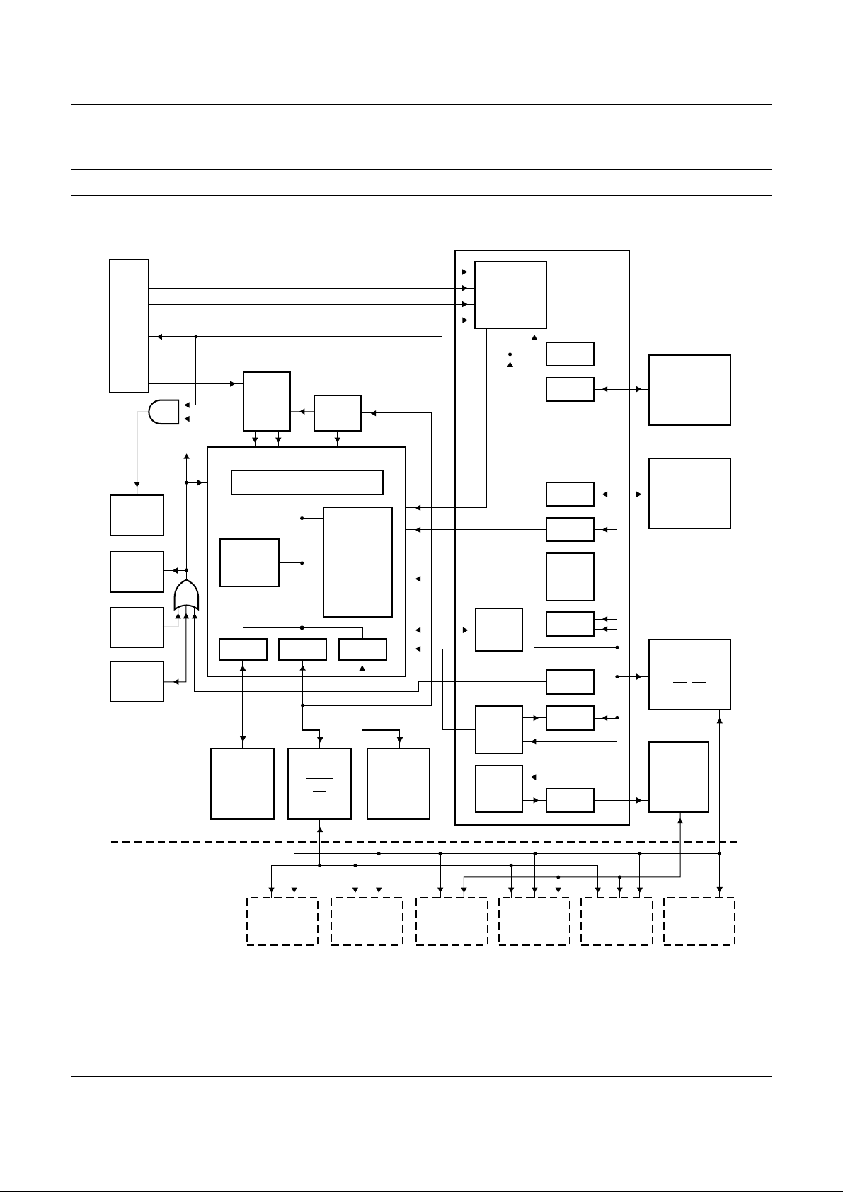
10 THE MICROCONTROLLER
The embedded MS80C51 microcontroller controls the
Digital Telephone Answering Machine (DTAM) chip by
means of Special Function Registers (SFRs). SFRs are
defined for the blocks MCB, TICB, PCON, DSP, I2C-bus,
ports P1, P3 and P4, MA, MSK and ANA (the analog
blocks). Allof these (except SFR PCON)are shown inthe
block diagram in Fig.1. The architecture of the
microcontroller itself and the interface to these blocks are
described in this chapter.
10.1 Microcontroller architecture
The microcontroller architecture and its environment is
shown in Fig.7.
The microcontroller has some application-specific
peripherals such as the I2C-bus, Watchdog Timer (WD),
P1, P3, P4,MCB, ExternalInterfacewith MA port,SFRsof
the DSPblock, theTICB andthe ANA block.Most ofthese
functions andSFRs are locatedin the ApplicationSpecific
Function block (ASF), see Fig.7.
The 80C51 core contains the 80C51 standard functions
such as Timer 0and Timer 1, power-down/idle states and
a 15 vector dual-level interrupt controller INT15L2.
Furthermore, the microcontroller contains the Metalink
enhanced hooks protocol which enables Metalink
emulation via ALE, PSEN, EA, P0 and P2. The external
programmemory accessis doneviathe standardPorts P0
and P2. Connection of external flash memory is done via
the P4, P0 and P2 I/O pads. The microcontroller Clock
Driver (CD) has no clock divider, which means that the
microcontroller operates on6microcontroller_CLKclocks
per machine cycle.
The 80C51 has a few basic modes of operation: Reset,
Normal, Metalink, Test (various) Idle and Power-down.
Entering the Metalink mode can be done via inputs ALE
and EA during a reset.
The Idle mode canbe entered by setting the IDL bit in the
PCON register. Leaving the Idle mode can be done via a
master reset (RSTIN), any external interrupt, a
DSP_event, TIME_event or RTC_event, Timer 0 and
Timer 1, I2C-bus interrupt, MSK_event or FS_event; if
these interrupts are enabled.
The Power-down mode can be entered by setting the
PD bit in PCON. The power-down logic of the
microcontroller will turn all microcontroller clocks off.
The TIME_event, DSP_event, RTC_event and
EX2 to EX6are mixedwith EX0(see Fig.10)and therefore
make use of the standard wake-upcircuitryof the 80C51.
These interrupts should be active for more than 6 clocks
(read, modify, write of IRQ1 takes 1 instruction) to
guarantee the interrupt for the microcontroller.
Setting the PD bitofPCON after setting the system-off bit
of SPCON, will trigger the analog section to turn off the
oscillator and therefore the whole chip. In order to keep
staticsupply currentsminimal, itis advisedtoswitch offthe
digital-to-analog part of the CODECs before going in this
system-off mode. Wake-up from system-off can be done
viaa RSTINor anexternal interruptEX0 to EX6(if theEX0
interrupt is enabled) or EX1 (if the EX1 interrupt is
enabled). A wake-upfromsystem-off will always resetthe
PCD6001. The EX interrupt condition should last more
than 4096 + 64 + 4 clocks to be sure that the interrupt is
handled whenentering the normal mode.If the interruptis
shorter themicrocontroller willonly enter thenormal mode
after the reset is gone.
10.2 Memory mapping
The memory map of the 80C51 is shown in Fig.8.
In addition to all the SFRs, the microcontroller has
128 bytes of directly addressable (DATA) memory,
128 bytes of indirectly addressable (IDATA) memory and
512 bytes of AUX RAM, the on-chip ‘MOVX’ addressable
(XDATA) memory. On-chip XDATA memory access can
be disabledby settingthe ARD bit inPCON tologic 1. The
internal32-kbyte ROMof microcontrollerprogram (CODE)
memory can be accessed when EA is set to logic 1.
Via Ports P0, MA, P2 and P4it is possible toaccess up to
512 kbytes of external speech data memory stored in a
parallel flash memory. A CAD flash memory can also be
mappedin thisarea. Aserial(SPI orMicrowire compatible)
flash memory can be connected to P4 which is controlled
by theMCB. Up to 64 kbytes ofprogram (CODE) memory
can beconnected to the P0, P2and PSEN pads.This can
be any external program memory (like the MON51 target
debug ROM) if EA is logic 0.
When the EAMSFR bit (P4CFG.5) is logic 0(default after
reset), the XRAM-mapped control registers can only be
accessed if P4.3 is logic 1. Otherwise, XRAM addressing
is independent of the value of the P4.3 SFR bit.
2001 Apr 17 20
Philips Semiconductors Product specification
Digital telephone answering machine chip PCD6001
handbook, full pagewidth
TICB
O PAD
DIS_XTAL
O PAD
MRST
I PAD
RST_ANA
I PAD
RST_IN
MRST
SPCON[7]
µC_CLK
osc_off
MODE
CONTROL
RAMIF
FS_event
RTC_event
TIME_event
DSP_event
TICBIF
CD
µCMS 80C51 CORE
CPU
XMEMU
MSEL
SF
GROUP INT.
TIMER 0
TIMER 1
PCON.0
to
PCON.1
INT15L2
ROMIF
pad_ale
pad_ea_n
IRQ1/IX1
DSP_req
2
I
C-bus_int
ARD
GROUP
WDRST
APPLICATION
SPECIFIC
FUNCTIONS
TICB
ANA
EX0 to EX6
DSP
I2C-BUS
PCON.2
to
PCON.7
PORT1
IF
WD
ANALOG
FUNCTIONS
DSP
I/O PADS
P1, P3
RD,WR
MSK_INT
SRAM
MAIN/AUX
RAM
256/512
BYTES
I/O PADS
EXTERNAL
64-kbyte
SRAM
P0, P2
PSEN
EA
ALE
INTERNAL
32 KBYTE
ROM
DRAM
ARAM
Fig.7 Microcontroller (MS 80C51) architecture and environment.
2001 Apr 17 21
FLASH
MICROWIRE/
SPI
MSK
MCB
FLASH
PARALLEL
PORT3
PORT4
FLASH
CAD
I/O PADS
P4
FLASH
2
I
C-BUS
MGT432
Philips Semiconductors Product specification
Digital telephone answering machine chip PCD6001
handbook, full pagewidth
255
XDATA-mapped registers
P4.3 = 1, EAM = 0, ARD = X
or ARD = 0, EAM = 1, EA = 1
Main RAM SFR
IDATA
Internal XDATA
518
515
ConfReg
512
AUX RAM
memory
P2
MA
64K
32K
External data
memory
XDATA
P4.3 = X
ARD = X
P4.3 = 0
ARD = 1
External program
memory
CODE
Internal ROM
CODE
128
48
ADDRESSABLE
32
REGISTER
BANKS 0 TO 3
0
DATA
BIT
SPACE
XDATA
ARD = 0
Fig.8 Microcontroller memory map.
2001 Apr 17 22
P4.3 = X
ARD = 1
EA = 1
EA = 1
MGT433
Philips Semiconductors Product specification
Digital telephone answering machine chip PCD6001
10.3 SFR mapping
The SFRmapping for themicrocontroller is shownin Table 12. All SFRsand their resetstates are describedin Table 13.
Table 12 SFR mapping
SFR
ADDRESS
(HEX)
F8 to FF IP1
F0 to F7 B
ADDRESSABLE
(2)
(2)
E8 to EF IEN1
E0 to E7 ACC
D8 to DF S1CON
D0 to D7 PSW
(1)
(2)
(2)
(2)
(2)
SPECIAL FUNCTION REGISTERS 8 BITS EACH
ONLY BYTE ADDRESSABLE
− −−−−−WDT
(2)
− −−−−−WDTKEY
IX1 −−−−−−
− −−−−−−
S1STA
(2)(3)
S1DAT
(2)
S1ADR
(2)
−−−−
− −−−−−−
C8 to CF MCON MBUF MSTAT −−−−−
REFR
(2)
(2)
(3)
GPADC GPDAR SYMOD − DTCON
(2)
(4)
− TCTRL
(4)
PMTR2
(4)
− P4CFG
−−
CDVC1 CDVC2 CDTR1
(3)
DTM1
(2)
TL1
DPH
(3)
DTM2
(2)
TH0
(2)
−−−PCON
(3)
MTD0 MTD1 MTD2
TH1
(4)
(4)
CDTR2
C0 to C7 IRQ1 INTC GPADR
(2)
(2)
(2)
XWUD V
−−−−PMTR1
MCSC MCSD ALTP −−−−
B8 to BF IP0
B0 to B7 P3
A8 to AF IEN0
A0 to A7 −−DTM0
98 to 9F P4 SPCON CKCON RTCON − CDTR1
90 to 97 P1
88 to 8F TCON
80 to 87 − SP
(2)
(2)
− −−−−−−
(2)
TMOD
(2)
TL0
DPL
Notes
1. SFRs in this column are both bit and byte-addressable.
2. Complies to 80C51 family architecture specification.
3. These registers are read only (all other SFRs are read/write).
4. Reserved register, used for testing purposes. Writing of reserved or undocumented bits might lead to unexpected
behaviour of the device (see Section 10.8).
(4)
2001 Apr 17 23
Philips Semiconductors Product specification
Digital telephone answering machine chip PCD6001
Table 13 Microcontroller register list
NAME ADDRESS (HEX) DESCRIPTION RESET STATE
ACC E0 accumulator 0000 0000
ALTP AB LE and GPC control X000 0000
A − accumulator 0000 0000
B F0 B register for multiply, divide or scratch 0000 0000
CKCON 9A Clock Control Register 0000 0000
CDVC1 BB CODEC digital volume control for CODEC1 00XX 0XXX
CDVC2 BC CODEC digital volume control for CODEC2 00XX 0XXX
CDTR1 BD CODEC Test Register 1; see note 1 00XX 0XXX
CDTR2 B7 CODEC Test Register 2; see note 2 00XX 0XXX
DTCON C7 line selection and alternative gain control register XX00 X00X
DPL 82 data pointer low 0000 0000
DPH 83 data pointer high 0000 0000
DTM0 A2 DSP to Microcontroller Communication Register 0 (read only) 0000 0000
DTM1 A3 DSP to Microcontroller Communication Register 1 (read only) 0000 0000
DTM2 A4 DSP to Microcontroller Communication Register 2 (read only) 0000 0000
GPADC C3 automatic analog-to-digital conversion, channel select, request
confirm
GPADR C2 digital value of analog input (read only) 0000 0000
GPDAR C4 digital value of analog output 1000 0000
IEN0 A8 Interrupt Enable Register 0 0000 0000
IEN1 E8 Interrupt Enable Register 1 0000 0000
INTC C1 Interrupt Control Register XXXX XX00
IP0 B8 Interrupt Priority Register 0 X000 0000
IP1 F8 Interrupt Priority Register 1 0000 0000
IRQ1 C0 Interrupt Request Flag Register 0000 0000
IX1 E9 Interrupt Polarity Register XXX0 0000
MCSD AA Memory Control Serial Data Register 0000 0000
MCSC A9 Memory Control Serial Command Register XXXX 0000
MTD0 A5 microcontroller to DSP communication register 0 0000 0000
MTD1 A6 microcontroller to DSP communication register 1 0000 0000
MTD2 A7 microcontroller to DSP communication register 2 0000 0000
MCON C8 MSK Control Register 0000 0000
MBUF C9 MSK Data Buffer Register XXXX XXXX
MSTAT CA MSK Status Register 0X00 0000
P1 90 general purpose digital I/O 1111 1111
P3 B0 general purpose digital I/O 1111 1111
P4 98 P4 can be used to control flash memory XX01 1110
P4CFG 9F P4 configuration and addressing mode register 0000 0000
PCON 87 Power and Interrupt Control Register X000 0000
PMTR1 B5 Power Management Test Register 1; see note 2 0000 0000
XXXX X000
(1)
2001 Apr 17 24

Philips Semiconductors Product specification
Digital telephone answering machine chip PCD6001
NAME ADDRESS (HEX) DESCRIPTION RESET STATE
PMTR2 B6 Power Management Test Register 2; see note 2 0000 0000
PSW D0 Program Status Word 0000 0000
RTCON 9B Real-Time Clock control 0000 0000
S1CON D8 I
S1ADR DB I
S1DAT DA I
S1STA D9 I
2
C-bus Serial Control Register 0000 0000
2
C-bus own slave address register 0000 0000
2
C-bus Data Shift Register 0000 0000
2
C-bus Status Register (read only) 1111 1000
SYMOD C5 analog system mode control 0000 0000
SPCON 99 system power and clock configuration 0XX0 0000
SP 81 Stack Pointer 0000 0111
TCON 88 Timer/counter Control Register 0000 0000
TMOD 89 Timer/counter Mode Control Register 0000 0000
TL0 90 Timer Low Register 0 0000 0000
TL1 91 Timer Low Register 1 0000 0000
TH0 92 Timer High Register 0 0000 0000
TH1 93 Timer High Register 1 0000 0000
VREFR BA Voltage Reference Register 1010 0000
WDT FF Watchdog Timer 0000 0000
WDTKEY F7 Watchdog Key Register 0000 0000
XWUD B9 external wake-up disable 0000 0000
(1)
Notes
1. All SFR bitswith reset state ‘X’ are either‘spare’ (i.e. have a memorybit in this position withreset state ‘0’) or‘-’(i.e.
do not haveaphysical memory bit in this position).All ‘spare’ bits can be addressedand used as additional general
purpose bits. All bits marked ‘-’ cannot be addressed by the user. To see which bits are ‘spare’ or ‘-’ refer to the
respective SFR layouts.
2. Reserved registers, used for testing purposes. Writing of undocumented or reserved bits might lead to unexpected
behaviour of the device (see Section 10.8).
2001 Apr 17 25

Philips Semiconductors Product specification
Digital telephone answering machine chip PCD6001
10.4 Microcontroller interrupts
The microcontroller has 15 interrupt sources, shown
below, which can be programmed to have a low or high
priority. If enabled these interrupts sources result in jump
to the addresses shown in Table 14.
• EX2 to EX6 asynchronous external interrupts via
P1.0 to P1.4
• EX0 and EX1 asynchronous external interrupts via
P3.2 (INT0N) and P3.3 (INT1N)
• DSP_event
• FS_event
• TIME_event
• I2C-bus interrupt
• RTC_event
• Timer 0 and Timer 1 interrupt
• MSK interrupt.
The external interrupt configuration of P1 is shown in
Fig.9. Pins P1.5, P1.6 and P1.7 cannot be used as
externalinterrupts. The IX1SFR determinesthe polarityof
the external interrupt sources of P1. Clearing the ‘global
enable’ bit in IEN0 disables all interrupt sources. Using
IEN0 (and IEN1) each individual external interrupt can be
enabled or disabled.
The IRQ1 SFR stores all external interrupts. So if an
external interrupt with a low priority is detected during
execution ofanother (highor lowpriority) interrupt itwill be
handled just after the return of this interrupt.
The interrupt serviceroutine for an externalinterrupt must
clear theright IRQ1 flag toindicate that it hasserviced the
interrupt request. Notice that during the interrupt routine
this flag can be set again immediately after clearing the
IRQ1 flag if the interrupt source is (still) HIGH.
The complete interrupt system is shown in Fig.10. All
15 interrupts are allocated and canbe given a low or high
priority according to the setting of IP0 and IP1.
Each interrupt source can be individually enabled by
means of IEN0 and IEN1.
The IRQ1 and IX.7 registersare clocked (a clock which is
active during Idle) and can be set by P1.0 to P1.4, the
TIME_event, the DSP_event, the FS_event and the
RTC_event. These flags canonly be cleared by software.
Only TCON.1, TCON.3, TCON.5 and TCON.7 flags are
cleared bythe interrupt controllerhardware. All otherflags
must be cleared by software.
The pollingof apotential interrupt goesfrom ahigh priority
to a low priority interrupt. Within a high (or low) priority
interrupt level the EX0(if set to high priority) will be polled
first followed by the next high priority interrupt.
Theinterrupt SFRsIP0, IP1,IEN0,IEN1, IRQ1andIX1 are
defined inSections 10.4.1 to 10.4.6. A flagset tologic 1 in
IP0 or IP1 (Tables 15 and 16) causes the corresponding
interrupt to have high priority.
2001 Apr 17 26

Philips Semiconductors Product specification
Digital telephone answering machine chip PCD6001
Table 14 Allocation of interrupt sources
VECTOR SOURCE NUMBER
(1)
PRIORITY
0003 EX0 0 1 external interrupt 0 IEN0.0/IP0.0
000B T0 1 4 Timer 0 interrupt IEN0.1/IP0.1
0013 EX1 2 7 external interrupt 1 IEN0.2/IP0.2
001B T1 3 10 Timer 1 interrupt IEN0.3/IP0.3
0023 MSK_event 4 13 MSK RI or TI interrupt IEN0.4/IP0.4
002B TIME_event 5 2 TIME interrupt IEN0.5/IP0.5
0033 FS_event 6 5 FS interrupt IEN0.6/IP0.6
003B EX2 7 8 external interrupt 2 IEN1.0/IP1.0
0043 EX3 8 11 external interrupt 3 IEN1.1/IP1.1
004B EX4 9 14 external interrupt 4 IEN1.2/IP1.2
0053 EX5 10 3 external interrupt 5 IEN1.3/IP1.3
005B EX6 11 6 external interrupt 6 IEN1.4/IP1.4
0063 I
2
C-bus 12 9 I2C-bus interrupt IEN1.5/IP1.5
006B DSP_event 13 12 DSP interrupt IEN1.6/IP1.6
0073 RTC_event 14 15 RTC interrupt IEN1.7/IP1.7
(2)
DESCRIPTION IENx/IPx
Notes
1. For some C-compilers ‘1’ has to be added to this number.
2. The interrupt controller supports up to 15 interrupt sources, each with a 2-level (high or low) priority. High priority
interrupt is always serviced before a low priority interrupt, but within the high and low levels, interruptsare serviced
in the order shown in this column.
handbook, full pagewidth
P1.7
P1.6
P1.5
P1.4
P1.3
P1.2
P1.1
P1.0
RTC_event
DSP_event
TIME_event
RTC
FS
TIME
EX6
EX5
EX4
EX3
EX2
IX1 IEN1
Fig.9 Port 1 external interrupt configuration.
2001 Apr 17 27
IRQ1
MGM773
Philips Semiconductors Product specification
Digital telephone answering machine chip PCD6001
handbook, full pagewidth
EXP1N + XWU
SOURCE
EX0
T0
EX1
T1
MSK
2
I
C-BUS
FS_event
EX2
EX3
EX4
EX5
EX6
TIME_event
DSP_event
RTC_event
IX.0
IX.1
IX.2
IX.3
IX.4
EDGE/LEVEL
TCON.0 TCON.1 IEN0.0
TCON.2
POLARITY
FLAGS ENABLE
TCON.5
TCON.3
TCON.7
MSTAT.0
MSTAT.1
S1CON.3
INTC.0
IRQ1.0
IRQ1.1
IRQ1.2
IRQ1.3
IRQ1.4
IRQ1.5
IRQ1.6
IRQ1.7
IEN0.1
IEN0.2
IEN0.3
IEN0.4
IEN0.5
IEN0.6
IEN1.0
IEN1.1
IEN1.2
IEN1.3
IEN1.4
IEN1.5
IEN1.6
IEN1.7
PRIORITY
IP0.0
IP0.1
IP0.2
IP0.3
IP0.4
IP0.5
IP0.6
IP1.0
IP1.1
IP1.2
IP1.3
IP1.4
IP1.5
IP1.6
IP1.7
INTERRUPT
SCANNING
INTERRUPT CONTROLLER
MGM774
XWUD
XWUD.0
to
XWUD.7
EXP1N
clocks
Fig.10 PCD6001/80C51 interrupt system.
10.4.1 INTERRUPT PRIORITY REGISTER 0 (IP0)
Table 15 Interrupt Priority Register 0 (SFR address B8H); reset state 00H
76 543210
−priority FS_event priority TIME priority MSK priority T1 priority EX1 priority T0 priority EX0
10.4.2 Interrupt Priority Register 1 (IP1)
Table 16 Interrupt Priority Register 1 (SFR address F8H); reset state 00H
76543210
priority RTC priority DSP priority I2C priority EX6 priority EX5 priority EX4 priority EX3 priority EX2
2001 Apr 17 28

Philips Semiconductors Product specification
Digital telephone answering machine chip PCD6001
10.4.3 INTERRUPT ENABLE REGISTER 0 (IEN0)
Table 17 Interrupt Enable Register 0 (SFR address A8H); reset state 00H
76543210
global
enable
enable
FS_event
enable TIME enable
MSK_event
enable T1 enable EX1 enable T0 enable EX0
10.4.4 I
NTERRUPT ENABLE REGISTER 1 (IEN1)
Table 18 Interrupt Enable Register 1 (SFR address E8H); reset state 00H
76543210
2
enable RTC enable DSP enable I
10.4.5 I
NTERRUPT REQUEST FLAG REGISTER (IRQ1)
C enable EX6 enable EX5 enable EX4 enable EX3 enable EX2
Table 19 Interrupt Request Flag Register 1 (SFR address C0H); reset state 00H; note 1
76543210
RTC flag DSP flag TIME flag EX6 flag EX5 flag EX4 flag EX3 flag EX2 flag
Note
1. The flags of IRQ1 will be set to logic 1 by hardware if the interrupt occurs. They must be cleared by software in the
interrupt service routine.
10.4.6 I
NTERRUPT POLARITY REGISTER (IX1)
Table 20 Interrupt Polarity Register (SFR address E9H); reset state 00H; note 1
76543210
spare spare spare polarity EX6 polarity EX5 polarity EX4 polarity EX3 polarity EX2
Note
1. A polarity bit set to logic 1 in IX1 will cause the external interrupt to be active HIGH.
10.4.7 I
NTERRUPT CONTROL REGISTER (INTC)
Table 21 Interrupt Control Register (SFR address C1H); reset state 00H
76543210
spare spare spare spare spare spare extended
FS flag
wake-up;
XWU
10.4.8 E
XTERNAL WAKE-UP DISABLE REGISTER (XWUD)
Table 22 External Wake-up Disable Register (SFR address B9H); reset state 00H
76543210
RTC XWU
disable
DSP XWU
disable
TIME XWU
disable
EX6 XWU
disable
EX5 XWU
disable
EX4 XWU
disable
EX3 XWU
disable
EX2 XWU
disable
2001 Apr 17 29
 Loading...