

INTEGRATED CIRCUITS
DATA SH EET
PCD5096
Universal codec
Preliminary specification
File under Integrated Circuits, IC17
1997 Jan 22

Philips Semiconductors Preliminary specification
Universal codec PCD5096
CONTENTS
1 FEATURES
2 GENERAL DESCRIPTION
3 APPLICATIONS
4 ORDERING INFORMATION
5 BLOCK DIAGRAM
6 PINNING INFORMATION
6.1 Pin description
6.2 Pinning
6.3 Supply concept
7 FUNCTIONAL DESCRIPTION
7.1 General
7.2 Clocking
7.3 Reset and power-down strategy
8 MEMORY AND CONTROL REGISTERS
8.1 DSP memories
8.2 Data memory and control register map
8.3 Control registers organization
9 IOM
9.1 Features
9.2 Pin description
9.3 Functional description
9.4 Timing
9.5 IOM control table
9.6 IOM data buffers
9.7 Local loop
10 I2C-BUS INTERFACE
11 CODEC TEST LOOPS
11.1 Test modes definition
11.2 Codec test loop signal timing
12 APPLICATION INFORMATION
12.1 Small business systems
12.2 Large business systems
12.3 DECT and ISDN
13 APPLICATION EXAMPLES
13.1 PCD5096 with two active channels
13.2 Conference call between one PSTN line and
two IOM buffers
13.3 Conference call between two PSTN lines and
one IOM buffer
14 LIMITING VALUES
15 HANDLING
16 ELECTRICAL SPECIFICATIONS
17 PACKAGE OUTLINE
18 SOLDERING
18.1 Introduction
18.2 Reflow soldering
18.3 Wave soldering
18.4 Repairing soldered joints
19 DEFINITIONS
20 LIFE SUPPORT APPLICATIONS
21 PURCHASE OF PHILIPS I2C COMPONENTS
1997 Jan 22 2

Philips Semiconductors Preliminary specification
Universal codec PCD5096
1 FEATURES
• Applications in digital terminal equipment featuring line
interface and/or voice functions
• Digital signal processor performing echo cancellation,
codec functions and dial tone detection
• Two independent receive and transmit channels
• Independent programmable gain for all analog inputs
and outputs
• Programmable filter correction functions
• Flexible configuration of all functions
• IOM-2 serial data interface (slave mode only)
• Serial data interface to DTAM speech compression ICs
2
• 400 kHz I
C-bus slave interface (four I2C-bus
subaddresses)
• Codec compatible with G.714 CCITT specification
• PCM A-Law/u-Law (G.711 CCITT) and 16-bit linear data
• Dual differential inputs and outputs performing the
following functions:
– Line interface connection
– Loudspeaker, speaker phone (hands-free)
– Earpiece, microphone (handset)
• Peripheral interface: two I/O pins
• Separate ringer function
• Tone and ringer generator
• Conference call
• QFP44 package
• Low voltage (2.7 to 3.6 V)
• Low power consumption.
2 GENERAL DESCRIPTION
The universal codec combines two high resolution
bidirectional analog channels with a DSP in a single chip.
Besides the analog interfaces the PCD5096 includes two
digital interfaces: an I
2
C-bus interface allowing an external
microcontroller to program the chip, and a 4-wire serial
interface compatible with IOM-2 and with DTAM speech
compression ICs. This programmable serial interface
offers up to 14 channels and is capable of handling 8-bit
(A-law) or 16-bit (linear PCM) data packages, or any
combination of them. It opens the scope for a wide
application area, for example in combination with the
PCD5093H DECT baseband chip for digital cordless
business applications.
Several PCD5096s can be connected together for small
switching systems (PABX) offering a combination of
corded and cordless functionality. Besides the basic
functions like echo cancellation for two channels the
on-chip DSP provides all necessary functions such as
conference call and DTMF.
3 APPLICATIONS
The PCD5096 is designed for the telecommunications
market and is targeting small business and residential
systems offering a two-line interface or a one-line interface
combined with hands-free speaker phone. Specific
applications are detailed in Chapter 12.
4 ORDERING INFORMATION
TYPE
NUMBER
NAME DESCRIPTION VERSION
PACKAGE
PCD5096H QFP44 plastic quad flat package; 44 leads (lead length 1.3 mm);
body 10 × 10 × 1.75 mm
1997 Jan 22 3
SOT307-2

Philips Semiconductors Preliminary specification
Universal codec PCD5096
5 BLOCK DIAGRAM
VREF1
MICM1
MICP1
LIFM_AD1
LIFP_AD1
LIFM_DA1
LIFP_DA1
EARP_HF
EARM_HF
EARP_HS
LIFM_AD2
LIFP_AD2
EARM_HS
MICP_HF
MICM_HS
MICP_HS
VMIC_HS
MICM_HF
VREF2
VMIC_HF
MBH864
SSA_1
V
DDA_1
V
SS_2
V
DD_2
V
s
108f
DIGITAL
s
4f
system bus
DAC
NOISE
SHAPER
DIO 1
s
108f
DIGITAL
s
4f
AMP1
ADC
FILTER
DECIMATING
DSP
CODEC 1
CORE
BIU
s
108f
DIGITAL
s
4f
DAC
NOISE
SHAPER
DIO 2
AMP2
ADC
s
108f
DIGITAL
DECIMATING
s
4f
ZROM
YRAM
XRAM
FILTER
4K × 24
512 × 16
512 × 16
CODEC 2
SYSTEM DATA
ANALOG
TCB
TIMING
CONTROL
PLL
RESET
GENERATOR
RAM
(SDRC)
CONTROLLER
VOLTAGE
REFERENCE
(TICB)
BLOCK
(RGE)
CONTROL
REGISTERS
SSA_2
V
DDA_2
V
TEST VBGP
SS_PLL
V
V
IO1 IO0 RESET CLK
handbook, full pagewidth
DD_PLL
Fig.1 PCD5096 block diagram.
DCL
FSC
IOM
DI
DO
C-bus
2
I
INTERFACE
A0
A1
SCL
SDA
1997 Jan 22 4
DD_1
V
SS_1
V
RAM
(SDR)
SYSTEM DATA
128 WORDS
Philips Semiconductors Preliminary specification
Universal codec PCD5096
6 PINNING INFORMATION
6.1 Pin description Table 1 QFP44 package
SYMBOL PIN I/O
(1)
IO0 1 I/O programmable I/O pin 0 (Schmitt trigger input, pull-up output)
IO1 2 I/O programmable I/O pin 1 (Schmitt trigger input, pull-up output)
CLK 3 I clock input
V
DD_PLL
V
SS_PLL
V
SS_1
V
DD_1
SCL 8 I I
SDA 9 I/O I
A0 10 I I
A1 11 I I
4 P 3 V analog supply for PLL
5 P analog ground supply for PLL
6 P peripheral ground supply
7 P 3 to 5 V peripheral supply
2
C-bus clock signal input (Schmitt trigger)
2
C-bus data signal
2
C-bus subaddress
2
C-bus subaddress
LIFM_DA1 12 O negative analog output from Codec 1 to line interface
LIFP_DA1 13 O positive analog output from Codec 1 to line interface
V
DDA_1
14 P 3 V analog supply for Codec 1
LIFM_AD1 15 I negative analog input to Codec 1 from line interface
LIFP_AD1 16 I positive analog input to Codec 1 from line interface
V
SSA_1
17 P analog ground supply for Codec 1
MICM1 18 I negative analog input to Codec 1 from microphone
MICP1 19 I positive analog input to Codec 1 from microphone
VREF1 20 O Codec 1 analog reference voltage
VBGP 21 O bandgap analog output voltage
VREF2 22 O Codec 2 analog reference voltage
VMIC_HS 23 O positive analog supply voltage from Codec 2 for handset microphone
MICP_HS 24 I positive analog input to Codec 2 from handset microphone
MICM_HS 25 I negative analog input to Codec 2 from handset microphone
VMIC_HF 26 O positive analog supply voltage from Codec 2 for hands-free microphone
MICP_HF 27 I positive analog input to Codec 2 from hands-free microphone
MICM_HF 28 I negative analog input to Codec 2 from hands-free microphone
V
SSA_2
29 P analog ground supply for Codec 2
LIFP_AD2 30 I positive analog input to Codec 2 from line interface
LIFM_AD2 31 I negative analog input to Codec 2 from line interface
V
DDA_2
32 P 3 V analog supply for Codec 2
EARP_HS 33 O positive analog output from Codec 2 to handset earpiece
EARM_HS 34 O negative analog output from Codec 2 to handset earpiece
EARP_HF 35 O positive output to hands-free earpiece
EARM_HF 36 O negative output to hands-free earpiece
TEST 37 I test input; pull-down
DESCRIPTION
1997 Jan 22 5
Philips Semiconductors Preliminary specification
Universal codec PCD5096
SYMBOL PIN I/O
(1)
DESCRIPTION
RESET 38 I reset input (Schmitt trigger)
V
V
SS_2
DD_2
39 P digital core ground supply
40 P 3 V digital core supply
DI 41 I IOM-2 interface serial data input
DO 42 O IOM-2 interface serial data output (open-drain)
FSC 43 I/O IOM-2 interface 8 kHz frame synchronization clock (Schmitt trigger input); note 2
DCL 44 I/O IOM-2 interface data clock (Schmitt trigger input); note 2
Note
1. ‘P’ denotes power line.
2. FSC and DCL are outputs only in test modes.
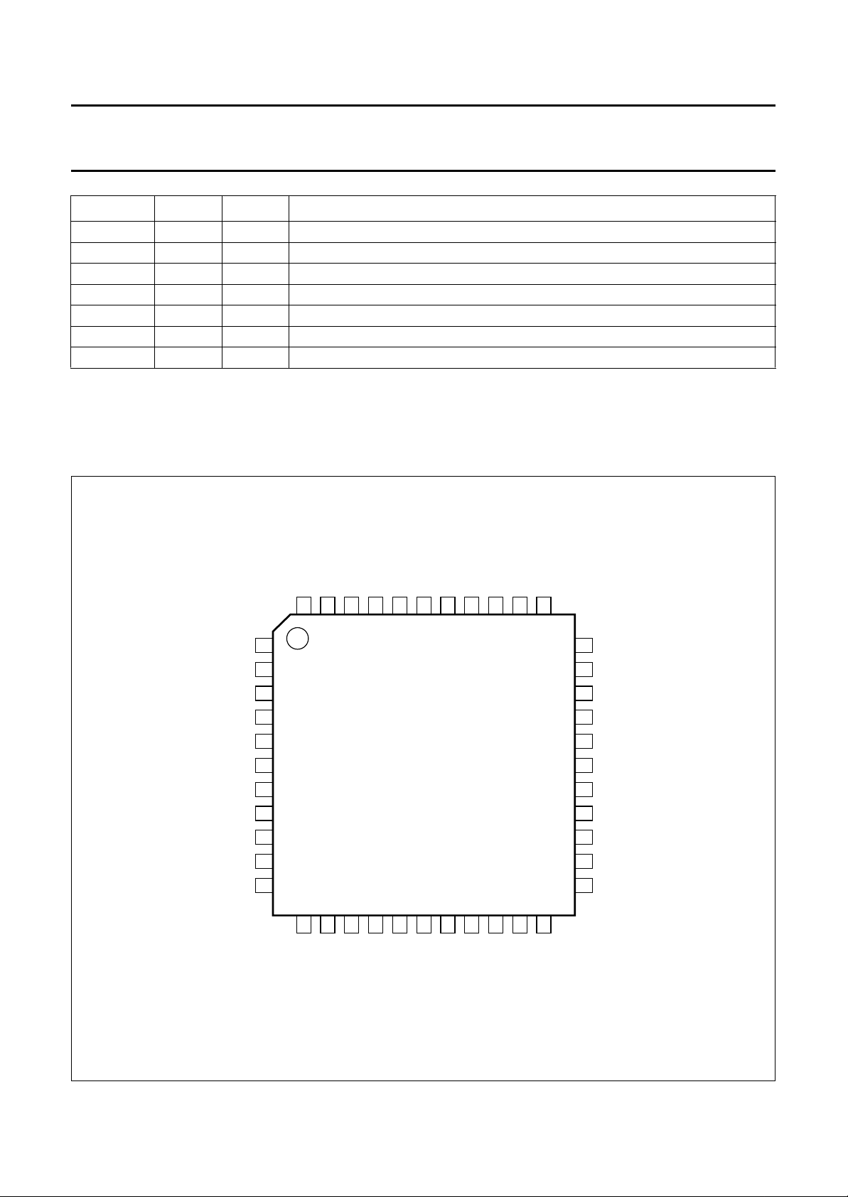
6.2 Pinning
handbook, full pagewidth
44 DCL
FSCDODI
43
42
41
DD_2VSS_2
V
40
39
RESET
38
TEST
37
EARM_HF
EARP_HF
36
35
EARM_HS
34
V
DD_PLL
V
SS_PLL
V
V
DD_1
IO1
CLK
SS_1
SCL
SDA
A0
A1
1IO0
2
3
4
5
14
DDA_1
PCD5096
15
16
LIFP_AD1
LIFM_AD1
17
SSA_1
V
18
MICM1
19
MICP1
20
VREF1
21
VBGP
22
VREF2
6
7
8
9
10
11
12LIFM_DA1
13
V
LIFP_DA1
33
32
31
30
29
28
27
26
25
24
23
MBH860
EARP_HS
V
DDA_2
LIFM_AD2
LIFP_AD2
V
SSA_2
MICM_HF
MICP_HF
VMIC_HF
MICM_HS
MICP_HS
VMIC_HS
Fig.2 Pin configuration.
1997 Jan 22 6

Philips Semiconductors Preliminary specification
Universal codec PCD5096
6.3 Supply concept
The universal codec is designed for 3 V systems with a voltage range of 2.7 to 3.6 V. To allow connection to 5 V systems
the digital I/Os include level shifters. The core must run on 3.3 V and the peripheral supply on 5 V.
The five power supplies are listed in Table 2. Codec 1 and Codec 2 have their own power supplies: V
respectively. V
and the digital peripherals by V
is the power supply dedicated to the PLL. The digital core and the memories are powered by V
DD_PLL
. All digital pins (EARP_HF, EARM_HF, TEST, RESET, DI, DO, FSC, DCL, IO0, IO1,
DD_1
DDA_1
and V
CLK, SCL, SDA, A0 and A1) have internal level shifters, allowing the chip to be used in a 3 to 5 V environment.
Table 2 PCD5096 power supply
SUPPLY PAIR ASSOCIATED DEVICE
V
and V
DD_1
V
DD_2
V
DD_PLL
V
DDA_1
V
DDA_2
handbook, full pagewidth
and V
and V
and V
and V
SS_1
SS_2
SSA_1
SSA_2
SS_PLL
3 to 5 V peripheral supply
3 V digital core supply
3 V PLL supply
3 V Codec 1 supply
3 V Codec 2 supply
V
DD_1
V
DD_2
V
DD_PLL
V
DDA_1
V
DDA_2
DDA_2
DD_2
V
SS_2
V
V
SS_1
SS_PLL
Fig.3 PCx5096 supply rails with protection diodes.
1997 Jan 22 7
V
SSA_1
V
SSA_2
MBH862

Philips Semiconductors Preliminary specification
Universal codec PCD5096
handbook, full pagewidth
V
DD_PLL
V
SS_PLL
V
V
DD_1
SS_1
DD_2VSS_2
V
substrate ring substrate ring
GND5 ring
GND ring
V
ring
DD5
VDD ring V
1
PLL
DIGITAL
CODEC 1
V
ring
DDA1
V
ring
SSA1
substrate ring
V
SSA2
DDA2
ring
ring
CODEC 2
MBH861
V
DDA_2
V
SSA_2
1997 Jan 22 8
DDA_1
V
SSA_1
V
Fig.4 PCD5096 power supply.

Philips Semiconductors Preliminary specification
Universal codec PCD5096
handbook, full pagewidth
V
DD_PLL
V
SS_PLL
V
V
IO1
CLK
SS_1
DD_1
SCL
SDA
FSC
DO
44 DCL
43
42
1IO0
2
3
4
5
6
7
8
9
DI
41
DD_2VSS_2
V
40
39
PCD5096
RESET
38
TEST
37
EARM_HF
36
EARP_HF
35
EARM_HS
34
33
32
31
30
29
28
27
26
25
EARP_HS
V
DDA_2
LIFM_AD2
LIFP_AD2
V
SSA_2
MICM_HF
MICP_HF
VMIC_HF
MICM_HS
A0
10
11
A1
12LIFM_DA1
13
14
15
16
DDA_1
V
LIFP_DA1
LIFM_AD1
LIFP_AD1
Fig.5 Open/short diagram.
1997 Jan 22 9
17
SSA_1
V
18
MICM1
19
MICP1
20
VREF1
21
VBGP
22
VREF2
MBH863
24
23
MICP_HS
VMIC_HS

Philips Semiconductors Preliminary specification
Universal codec PCD5096
7 FUNCTIONAL DESCRIPTION
7.1 General
The PCD5096 is a universal codec designed for use in
digital terminal equipment. It connects two PSTN lines to a
digital interface (IOM-2), thus covering a wide application
area. Echo cancellation is performed on both PSTN lines
by an on-chip DSP. Hands-free speaker phone
functionality is also provided by sacrificing one PSTN line
connection. The chip is controlled by an external
microcontroller via a high bit rate I
2
C-bus interface.
Figure 1 shows the block diagram of the PCD5096.
The different functional blocks operate more or less
autonomously and communicate with each other via the
System Data RAM (SDR). Each block has access to the
SDR via an internal system bus. Access to this bus is
controlled by the System Data RAM Controller (SDRC).
The IOM block connects to a n × 256 kbits/s digital
interface (IOM-2 interface) and also supports interfacing to
DTAM speech compression ICs. The IOM block stores
and fetches speech data into/from the SDR using internal
addressing logic.
The DSP block is the link between the data in the SDR
stored/fetched by the IOM block on one hand, and the
analog front-end on the other hand. The basic functions of
the DSP are data filtering, local echo cancelling, network
echo suppressing, A-law coding and decoding according
to the G.711 CCITT recommendations, dial tone detection
and generation, DTMF generation, side-tone, automatic
volume control, automatic gain control, double talk
detection and conference call.
Data processed by the DSP goes to and comes from two
independent codecs interfacing to the PSTN lines.
The codecs comply with the G.714 specifications and
handle the PCM coding and decoding of speech signals.
They perform the analog and high speed digital speech
processing functions: analog bitstream A/D and D/A
conversion, analog filtering and amplification, digital
decimation filtering and noise shaping. Both codecs
should be connected to a local line or to a PSTN line, but
one codec also supports a corded handset and hands-free
speaker and microphone.
The control of the entire chip is done via the I2C-bus block
by writing to the SDR or to special control registers. In this
way the DSP and the IOM operation modes can be set, as
well as some analog parameters in the two codecs.
The PCD5096 has two general purpose programmable I/O
pins controlled by two special registers (direction and
state). These two special registers are accessible via the
2
I
C-bus interface or by the on-chip DSP. A typical
application is the generation of interrupts by the DSP,
indicating that DTMF tones were detected.
The timing for the whole chip is generated in the Timing
Control Block (TICB). The system clock (20.736 MHz) is
delivered by a PLL which triples the input clock frequency.
7.2 Clocking
The universal codec is designed to operate in a digital
cordless telephone system, for example together with a
PCD5093 baseband controller. To save the expense of
having to provide each universal codec with a separate
crystal, a common clock is provided by the master
controller. In the current generation of the Philips DECT
baseband controllers this clock is GP_CLK7, a 6.912 MHz
clock output derived from the 13.824 MHz crystal
oscillator. GP_CLK7 must therefore be used as the input
clock for the universal codec. GP_CLK7 is enabled during
a reset of the PCD5093 and when either the Burst Mode
Logic or codec are turned on (see PCD5093 data sheet).
In order to meet the DSP processing requirements for the
various applications an on-chip PLL is used to generate a
system clock which is triple the input clock frequency
(20.736 MHz).
7.3 Reset and power-down strategy
The universal codec must be reset at power-up.
The RESET input must remain HIGH until the CLK input is
active (toggling) and stable. After releasing the RESET
input, an additional 1024 CLK periods (≈150 µs at
6.912 MHz) must elapse before starting to program the
2
chip via the I
C-bus interface. This must be done after
every RESET pulse. The minimum duration of a RESET
pulse is one CLK period. During reset, the I2C-bus and the
IOM-2 interface are inactive.
Entering the Power-down mode is achieved by resetting
the chip and holding the RESET input HIGH. This resets
the on-chip PLL and stops the system clock. The user
must ensure that the IOM-2 interface is deactivated and
the I2C-bus idle before resetting the chip in order not to
interrupt any transaction on these two interfaces. Note that
stopping the CLK input is only allowed while the RESET
input is HIGH. To exit the Power-down mode the RESET
input is set LOW and after 1024 CLK periods (≈150 µs at
6.912 MHz) have elapsed normal operation can be
resumed.
1997 Jan 22 10

Philips Semiconductors Preliminary specification
Universal codec PCD5096
After reset, all the flip-flops are in a defined state, and the
IOM, DSP and codecs are in inactive mode. In typical
applications the universal codec is used with the
PCD5093, which provides a clock (GP_CLK7) and a reset
signal to the universal codec. The reset signal must be
generated by a microcontroller port bit. The RESET_OUT
pin of the PCD5093 cannot be used for this purpose,
because GP_CLK7 is stopped while RESET_OUT is LOW
after a Power-on-reset.
8 MEMORY AND CONTROL REGISTERS
8.1 DSP memories
The DSP in the PCD5096 has access to a 4k × 24-bit DSP
program ROM, a 512 × 16-bit XRAM and a 512 × 16-bit
YRAM.
8.2 Data memory and control register map
The PCD5096 contains a 128 word (128 × 16-bit) System
Data RAM (SDR) and a group of 7 control registers
mapped onto the upper addresses of the SDR.
The registers and the SDR are byte and word accessible
externally, via the I
2
C-bus interface and internally via the
internal system bus.
The memory map is shown in Fig.6. The lower 32 words
contain the DSP parameter table. The next 32 words are
reserved for the IOM control table, which is used to control
the activity on the IOM-2 interface (maximum 32 slots per
8 kHz speech frame). The rest of the SDR addressable
space (40H to 77H) is free RAM and can be used to store
up to 14 IOM data buffer pairs. In cases where not all
14 IOM buffer pairs are needed this memory space can be
2
used for other applications via the I
C-bus. The same
holds for the unused part of the IOM control table.
The upper addresses of the SDR (78H to 7EH) are
mapped onto 7 control registers (CR0 to CR6) that control
the entire chip (DSP mode, data rate on the IOM-2
interface, control of the two codecs).
Note that the uppermost address of the SDR (7FH) is not
mapped to any hardware register and is addressable as a
normal RAM word.
The contents of the IOM control table and the IOM data
buffers are described in Chapter 9. For further details
about the DSP parameter table, see the
user manual”
.
“PCD5096 DSP
handbook, full pagewidth
7FH
7EH
78H
77H
40H
3FH
20H
1FH
00H
free RAM
control registers
(7 words)
IOM data buffers
and
free RAM
(14 x 4 words)
IOM control table
(32 words)
DSP parameter table
(32 words)
MBH865
Fig.6 PCD5096 Memory map.
SDR
hardware registers
SDR
1997 Jan 22 11
Philips Semiconductors Preliminary specification
Universal codec PCD5096
8.3 Control registers organization
8.3.1 C
The control register address assignment in the PCD5096 is shown in Table 3.
Table 3 Control register map
Control Register 0 CR0 16 78 0000 control signals for codecs, codec test
Control Register 1 CR1 3 79 00 IOM control
Control Register 2 CR2 16 7A 0000 gain setting of analog-to-digital (A/D) and
Control Register 3 CR3 16 7B A0A0 reference voltage setting of Codec 1 and
Control Register 4 CR4 16 7C 0000 selection of the DSP modes
Control Register 5 CR5 2 7D 02 control of I/O pin IO0
Control Register 6 CR6 2 7E 02 control of I/O pin IO1
ONTROL REGISTER ASSIGNMENT
REGISTER
REGISTER
MNEMONIC
SIZE
(BITS)
ADDRESS
(HEX)
RESET ST ATE
(HEX)
FUNCTION
modes, Power-down control and disable
phase correction
digital-to-analog (D/A) paths
Codec 2
1997 Jan 22 12

Philips Semiconductors Preliminary specification
Universal codec PCD5096
8.3.2 CONTROL REGISTER 0 (CR0)
Table 4 Control Register 0 (address 78H)
15 14 13 12 11 10 9 8
− DISPC CDC2TM2 CDC2TM1 CDC2TM0 CDC1TM2 CDC1TM1 CDC1TM0
Table 5 Control Register 0 (continued)
76543210
HFMICON HSMICON LHFEN EHSEN CDC2ON ADD_DC LIF1_EN CDC1ON
Table 6 Description of CR0 bits
BIT SYMBOL DESCRIPTION
15 − reserved, not used
14 DISPC Disable Phase Correction. If DISPC = 1, phase correction is disabled.
13 CDC2TM2 Functional test modes of Codec 2. These 3 bits select the functional test modes of
12 CDC2TM1
11 CDC2TM0
10 CDC1TM2 Functional test modes of Codec 1. These 3 bits select the functional test modes of
9 CDC1TM1
8 CDC1TM0
7 HFMICON Hands-free Microphone ON in Codec 2. When this bit is set the internal microphone
6 HSMICON Handset Microphone ON in Codec 2. When this bit is set the internal microphone
5 LHFEN Loudspeaker Enable for hands-free. This bit enables the Noise Shaper data in
4 EHSEN Earpiece Enable for Handset. This bit enables the Noise Shaper data to the DAC in
3 CDC2ON Codec 2 ON. When CDC2ON = 1, Codec 2 is ON.
2 ADD_DAC Add a DC offset in the microphone amplifier of Codec 1.
1 LIF1_EN Line Interface Enable for Codec 1. This bit enables the Noise Shaper data to the DAC
0 CDC1ON Codec 1 ON. When CDC1ON = 1, Codec 1 is ON.
Codec 2; see Table 7.
Codec 1; see Table 7.
reference voltage VREFMIC is connected to pad VMIC_HF (supply pad for the external
hands-free microphone).
reference voltage VREFMIC is connected to pad VMIC_HS (supply pad for the external
handset microphone).
Codec 2 to the hands-free pads EARP_HF and EARM_HF.
Codec 2.
in Codec 1.
1997 Jan 22 13
Philips Semiconductors Preliminary specification
Universal codec PCD5096
Table 7 Selection of functional test modes for Codec 1 and Codec 2
CDC2TM2 CDC2TM1 CDC2TM0
FUNCTIONAL TEST MODE
CDC1TM2 CDC1TM1 CDC1TM0
0 0 0 normal operation
0 0 1 1 bit analog
0 1 0 1 bit digital
0 1 1 1 bit closed loop
1004f
1014f
1104f
codec
s
DSP
s
closed loop
s
1 1 1 PCM probe
8.3.3 C
ONTROL REGISTER 1 (CR1)
Table 8 Control Register 1 (address 79H)
210
IOM2 IOM1 IOM0
Table 9 Description of CR1 bits
BIT SYMBOL DESCRIPTION
2 IOM2 These 3 bits select the IOM mode; see Table 10.
1 IOM1
0 IOM0
Table 10 Selection of IOM mode
IOM2 IOM1 IOM0 IOM MODE
0 0 0 inactive
0 0 1 not used
0 1 0 IOM slave 256 kbits/s in 4 speech-slots/speech-frame
0 1 1 IOM slave 512 kbits/s in 8 speech-slots/speech-frame
1 0 0 IOM slave 768 kbits/s in 12 speech-slots/speech-frame
1 0 1 IOM slave 1024 kbits/s in 16 speech-slots/speech-frame
1 1 0 SpeechPro slave 2048 kbits/s in 32 speech-slots/speech-frame; note 1
1 1 1 IOM slave 2048 kbits/s in 32 speech-slots/speech-frame
Note
1. The SpeechPro mode is similar to the IOM slave 32 slots mode, but with a non-doubled data clock DCL.
1997 Jan 22 14

Philips Semiconductors Preliminary specification
Universal codec PCD5096
8.3.4 CONTROL REGISTER 2 (CR2)
CR2 contains the gain setting values of the analog Codec 1 and Codec 2 section. The state of CR2 after reset is 0000H.
This sets the A/D path and the D/A path gain to their minimum values of +9 dB and −13 dB respectively.
The D/A path gain is defined as the relationship between the level of the analog output signal, differentially seen at
EARP_HS - EARM_HS or LIFP_DA1 - LIFM_DA1, expressed in dBm (0 dBm0 is 1 mW in 600 Ω), and the level of the
digital input signal at the PCM interface, expressed in dBm0 according to CCITT Recommendation G.711. This D/A path
gain definition assumes that the volume control in the DSP is set to the default value of 0 dB.
The A/D path gain is defined as the relationship between the level of the digital output signal at the PCM interface,
expressed in dBm0, and the level of the analog input signal at the LIF interface, differentially seen at
LIFP_AD2 - LIFM_AD2 or LIFP_AD1 - LIFM_AD1, expressed in dBm.
Table 11 Control Register 2 (address 7AH)
15 14 13 12 11 10 9 8
DA2.3 DA2.2 DA2.1 DA2.0 AD2.3 AD2.2 AD2.1 AD2.0
Table 12 Control Register 2 (continued)
76543210
DA1.3 DA1.2 DA1.1 DA1.0 AD1.3 AD1.2 AD1.1 AD1.0
Table 13 Description of CR2 bits
BIT SYMBOL DESCRIPTION
15 DA2.3 These 4 bits select the D/A path gain for Codec 2; see Table 14.
14 DA2.2
13 DA2.1
12 DA2.0
11 AD2.3 These 4 bits select the A/D path gain for Codec 2; see Table 15.
10 AD2.2
9 AD2.1
8 AD2.0
7 DA1.3 These 4 bits select the D/A path gain for Codec 1; see Table 14.
6 DA1.2
5 DA1.1
4 DA1.0
3 AD1.3 These 4 bits select the A/D path gain for Codec 1; see Table 15.
2 AD1.2
1 AD1.1
0 AD1.0
1997 Jan 22 15

Philips Semiconductors Preliminary specification
Universal codec PCD5096
Table 14 Selection of D/A path gain for Codec 1 and Codec 2
DA1.3 DA1.2 DA1.1 DA1.0
DA2.3 DA2.2 DA2.1 DA2.0
0000 −13
0001 −12
0010 −11
0011 −10
0100 −9
0101 −8
0110 −7
0111 −6
1000 −5
1001 −4
1010 −3
1011 −2
1100 −1
1101 0
1110 +1
1111 +2
Table 15 Selection of A/D path gain for Codec 1 and Codec 2
D/A PATH GAIN
(dB)
AD1.3 AD1.2 AD1.1 AD1.0
AD2.3 AD2.2 AD2.1 AD2.0
0000 +9
0001 +10
0010 +11
0011 +12
0100 +13
0101 +14
0110 +15
0111 +16
1000 +17
1001 +18
1010 +19
1011 +20
1100 +21
1101 +22
1110 +23
1111 +24
A/D PATH GAIN (FROM LIF TO PCM)
(dB)
1997 Jan 22 16
 Loading...