Philips PCD5091H, PCD5091HZ Datasheet

0 (0)

INTEGRATED CIRCUITS

DATA SHEET

PCD5091

DECT baseband controller

Objective specification

1997 Jul 21

Supersedes data of 1996 Oct 30

File under Integrated Circuits, IC17

Philips Semiconductors

Objective specification


DECT baseband controller

PCD5091


CONTENTS


1

FEATURES


1.1DSP software features

2GENERAL DESCRIPTION

3ORDERING INFORMATION

4BLOCK DIAGRAM

5PINNING INFORMATION

5.1Pinning

5.2Pin description

6FUNCTIONAL DESCRIPTION

7PACKAGE OUTLINES

8SOLDERING

8.1Introduction

8.2Reflow soldering

8.3Wave soldering

8.4Repairing soldered joints

9DEFINITIONS

10LIFE SUPPORT APPLICATIONS

11PURCHASE OF PHILIPS I2C COMPONENTS

1997 Jul 21

2


Philips Semiconductors

Objective specification


DECT baseband controller

PCD5091

1 FEATURES

80C51 ports P0, P1, P2 and P3 available for interfacing to display, keyboard, I2C-bus, interrupt sources and/or external memory. Integrated 64 kbyte ROM, 3 kbytes of data memory and 1 kbyte SDR-RAM. External program memory is addressable up to 128 kbytes

+2.7 to +5 V port (P0 to P3) interface

TDMA frame (de)multiplexing. Transmission or reception can be programmed for any slot

Ciphering, scrambling, CRC checking/generation and protected B-fields

Speech and data buffering space for six handsets

Local call and B-field loop-back

Two interrupt lines for BML and DSP to interrupt 80C51

On-chip, three-channel time-multiplexed 8-bit Analog-to-Digital Converter (ADC) for RSSI measurement, one for battery voltage measurement and one channel available for other purposes

On-chip 8-bit Digital-to-Analog Converter (DAC) for electronic potentiometer function

Phase error measurement and phase error correction by hardware

DACs and ADCs for dynamic earpiece and dynamic or electret microphone

On-chip reference voltage

On-chip supply for electret microphone

Very low ohmic buzzer output

Serial interface to external ADPCM CODEC (PCD5032) or 8 kHz u-law samples

Speech switch for Digital Telephone Answering Machine (DTAM) connected to SPI interface

IOM-2 interface (Siemens registered trademark)

Serial interface to synthesizer for frequency programming

Programmable polarity and timing of radio-control signals

GMSK pulse shaper

3 ORDERING INFORMATION
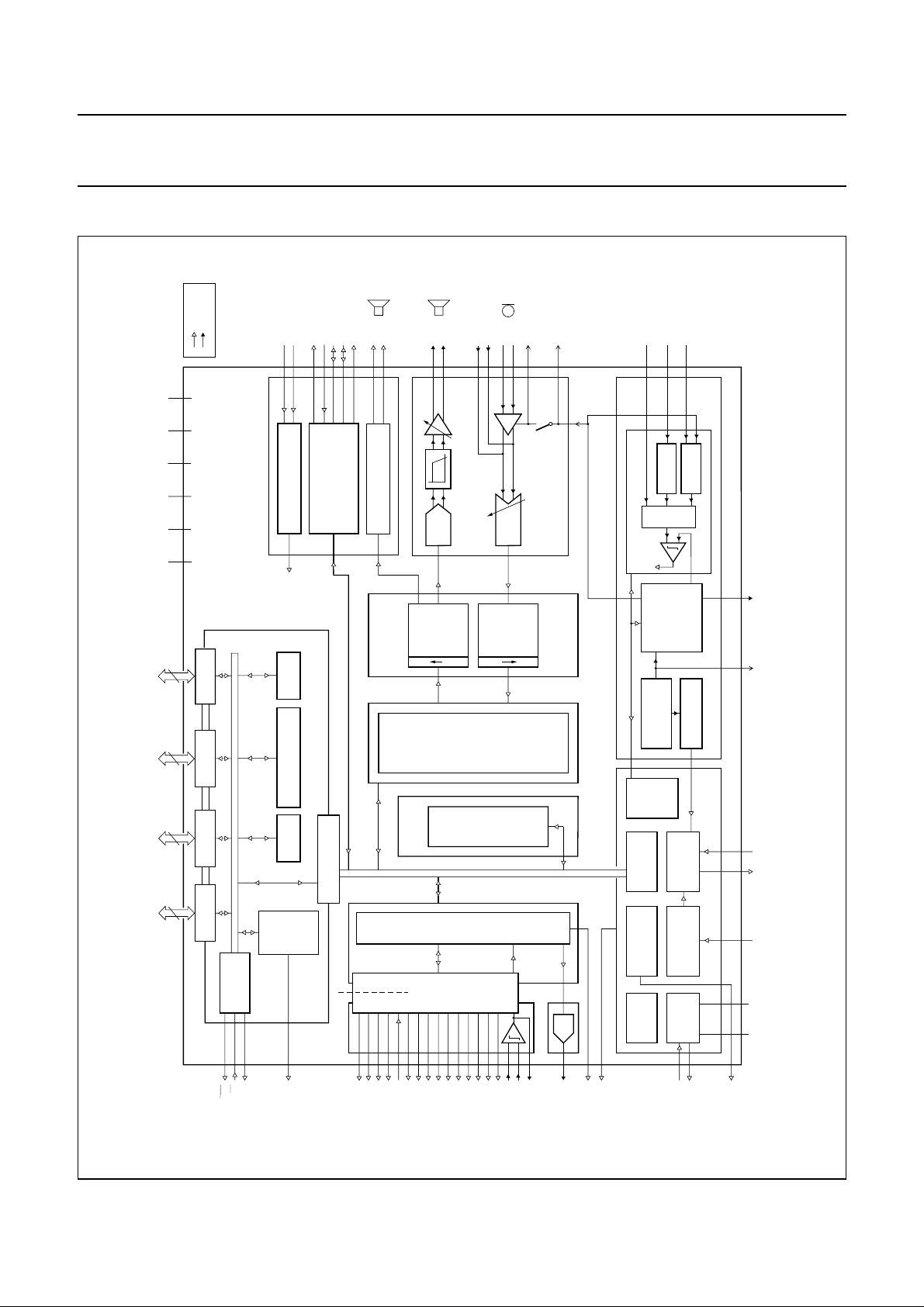
Easy interfacing with radio circuits, operating at other supply voltage (RF supply pin with level shifter for RF signals)

On-chip comparator for use as data-slicer

Low power oscillator with integrated frequency adjustment

QFP100 and LQFP100 packages

Power-on-reset

Programmable power-down modes

Low supply voltage (2.7 to 3.6 V)

CMOS technology.

1.1DSP software features

ADPCM encoding and decoding complying with G.721

Volume control

Speech filters

Programmable gain in speech paths

Side tone and soft mute

Two tone (DTMF) generators

Automatic gain control

Hands-free operation

For each DSP software version a separate manual is available in which detailed information is provided on how parameters must be set. For further information please contact Philips Semiconductors.

2 GENERAL DESCRIPTION

The PCD5091 is designed for GAP-compliant handsets with speaker-phone option. It has an embedded 80C51 microcontroller with twice the performance of the classic architecture, 64 kbytes of PROM program memory and 3 kbytes of data memory on-chip. In addition there is

1 kbyte of on-chip data memory that is shared with on-chip Burst Mode Logic (BML) and DSP, the System Data RAM (SDR).

TYPE


PACKAGE


NUMBER

NAME

DESCRIPTION

VERSION


PCD5091H

QFP100

plastic quad flat package; 100 leads (lead length 1.95 mm);

SOT317-2


body 14 × 20 × 2.8 mm


PCD5091HZ

LQFP100

plastic low profile quad flat package; 100 leads; body 14 × 14 × 1.4 mm

SOT407-1


1997 Jul 21

3

Philips PCD5091H, PCD5091HZ Datasheet

1997Jul21


PORT 0.0 to


PORT 1.0 to


PORT 2.0 to


PORT 3.0 to


5 ×

2 ×


3 ×


DIAGRAMBLOCK4

basebandDECT

SemiconductorsPhilips


PORT 0.7


PORT 1.7


PORT 2.7


PORT 3.7


VDD_RF

VSS

VDD3V

VSSA

VDDA

VDD5V


8


8


8


8


VDD


digital pins


PORT 0


PORT 1


PORT 2


PORT 3


analog pins


PSE


IB-BUS


PCD5091


EA


80CL51CORE


ALE


VDD


controller


A16


ROM


AUX-RAM

MICROCONTROLLER-RAM

I2C-BUS


TEST CONTROL BLOCK


TST1


(64 kBYTES)


(3 kBYTES)


(256 BYTES)


(TCB)


TST2


MICROCONTROLLER


DO


AB-MICROCONTROLLER


SPEECH INTERFACE


DI


VDD_RF


VDD


INTERFACE (ABCIF)


IOM/ADPCM


FS1


(SPI)


DCK


SLICE_CTR


VDD


VDD


CLK3


R_PWR


BUZZER BUFFER


BZP


R_ENABLE


(ABB)


BZM


REF_CLK


VDD


SYNTH_LOCK


S_ENABLE


VDDA


S_CLK


DIGITAL


S_DATA


LEVEL


4fs

108fs


EARP


NOISE


VCO_BND_SW


1-BIT ADC


SHIFTER


SHAPER


EARM


S_PWR


BURST


(DNS)


MODE


4

ANT_SW0


ARD


ARF

ARA


DIGITAL


LOGIC


ANT_SW1


SIGNAL


(BML)


SYSTEM


T_ENABLE


PROCESSOR


LIFP


T_PWR_RMP


DATA


(DSP)


LIFM


RAM


DIGITAL


T_DATA


(SDR)


4fs

108fs

Σ


MICP


DECIMATING


R_DATAP


(1 kBYTE)


FILTER


1-BIT ADC


MICM


R_DATAM


AMP


(DDF)


ATS


VMIC


R_SLICED


VDDA


CDC-on


T_GMSK

AGM


CODEC


Vref


DPLL_DATA


GP_CLK7

VDD


VDDA


CLOCK

TIMING CONTROL


ISB BUS

DIGITAL


AUXILIARY ADC (AAD)


GENERATOR

BLOCK


CONTROLLER

CONTROL

ANALOG VOLTAGE

Vref


VANLI


(CLG)

(TICB)


(IBC)

OF


ANALOG


REFERENCE

ANALOG


(AVR)


MUX


VOLTAGE


PEAK-HOLD


RSSI_AN


(DCA)


XTAL

WATCHDOG


RESET


3 : 1


SOURCE


XTAL1


OSCILLATOR

TIMER


GENERATOR


POWER-ON-RESET

(AVS)


VBAT


XTAL2

(XOSC)

(WDT)


(RGE)


VADC


SUBTRACT


(POR)


Vref


specification Objective


CLK100


VDDO

VSSO

EN_WATCHDOG

RESET_OUT

M_RESET


VBGP

VANLO


MGD800


Fig.1

Block handbook,fullpagewidthdiagram.


PCD5091


Philips Semiconductors

Objective specification


DECT baseband controller

PCD5091


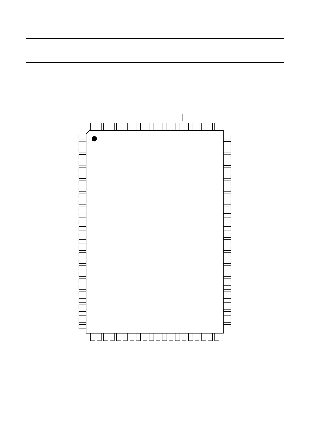
5 PINNING INFORMATION

5.1Pinning


RESETOUT


RESETM


P0.0


P0.1


P0.2


P0.3


P0.4


P0.5


P0.6


P0.7


V


V


EA


ALE


PSE


P2.7


P2.6


P2.5


P2.4


P2.3


DD5V3


SS5


100


99


98


97


96


95


94


93


92


91


90


89


88


87


86


85


84


83


82


81


ANT_SW1

1


80

TST2


ANT_SW0

2


79

TST1


CLK100

3


78

VSS4


T_ENABLE

4


77

VDD5V_2


T_PWR_RMP

5


76

A16


T_DATA

6


75

P2.2

T_GMSK


7


74

P2.1


VCO_BND_SW

8


73

P2.0

SYNTH_LOCK


P3.7

9


72

S_ENABLE


P3.6

10


71

S_DATA


P3.5

11


70

S_CLK


P3.4

12


69

S_PWR


P3.3

13


68

REF_CLK


P3.2

14


67

VSS1


P3.1

15


PCD5091


66

VDD_RF


P3.0

16


65

VDD3V_1


VSS3

17


64

SLICE_CTR


VSS2

18


63

R_PWR


BZP

19


62

R_DATAP


BZM

20


61

R_DATAM


VDD3V_2

21


60

R_ENABLE


P1.7

22


59

RSSI_AN


P1.6

23


58

VANLI


P1.5

24


57

VBAT


P1.4

25


56

CLK3


P1.3

26


55

DCK


VDD5V_1

27


54

DI


28


53

R_SLICED

FS1


DPLL_DATA

29


52

DO


GP_CLK7

30


51

31


32


33


34


35


36


37


38


39


40


41


42


43


44


45


46


47


48


49


50


XTAL2


XTAL1


VANLO


SSO

DDO

LIFM


LIFP


SSA

MICM


MICP


VMIC


ref


VBGP


DDA


EARM


EARP


WATCHDOG


P1.0


P1.1


P1.2


V

V


V


V


V


EN_


Fig.2 Pin configuration (QFP100).

MBH938

1997 Jul 21

5

Loading...
+ 11 hidden pages