

Philips pcd3316 DATASHEETS

PCD3316
Caller-ID on Call Waiting (CIDCW) receiver
11 March 1999 Product specification
1. General description
The PCD3316 is a low power mixed signal CMOS integrated circuit for receiving
physical layer signals like Bellcore’s ‘CPE1 Alerting Signal (CAS)’ and the signals
used in similar services. The device is capable of a very high precision detection of
the dual tone (2130 and 2750 Hz) by using a patented digital algorithm. The
Unrestricted
PCD3316 can be used for on-hook and off-hook Caller-ID (CID), Caller-ID on Call
Waiting (CIDCW) and Caller-Name (CNAM) applications.
For timing purposes the PCD3316 can be programmed to generate an interrupt
signal to themicrocontroller every second or every minute. These timings are derived
from an on-chip 32.768 kHz oscillator.
Also incorporated in the device are a Frequency Shift Keying (FSK)
receiver/demodulator and a ‘Ring or polarity change detector’. The status of the
PCD3316, the received FSK data bytes and the ringer period can be read and many
options can be selected via the I2C-bus serial interface. Two on-chip oscillators are
available. One 3.58 MHz oscillator for all internal functions and a low frequency
32.768 kHz oscillator for the 1 second or 1 minute timing.
In Power-down mode only the polarity comparators and the 32.768 kHz oscillator are
c
c
active. The CAS detection, the FSK receiver and the 3.58 MHz oscillator can be
enabled separately. Detection of a polarity change on the inputs POL0 or POL1, the
reception of an FSK data byte, the detection of a CAS tone or a timebase interrupt is
signalled to the microcontroller by an interrupt request signal (IRQ). The
microcontroller can communicate with the PCD3316 device via the serial interface.
The PCD3316 is designed for use in a microcontroller controlled system. The device
is available in a SO16 package.
A demonstration board OM5843 and an application note
AN98071
are available.
1. CPE = Customer Premises Equipment.

Philips Semiconductors
2. Features
■ Bellcore’s ‘CPE Alerting Signal (CAS)’ and British Telecom’s (BT) ‘Loop State
Unrestricted
■ BT’s ‘Idle State Tone Alert Signal’ by means of monitoring the input signal level
■ 1200 baud FSK demodulator conform Bell 202 and CCITT V23 standards
■ Ring or polarity change detector
■ Ring period measurement
■ Low battery comparator
■ Signal level detector
■ On-hook and off-hook applications according to
■ Receive sensitivity of −37.8 dBm (in 600 Ω) for CAS
■ 2.5 to 3.6 V supply; low power standby mode
■ Selectable 1 second or 1 minute timebase interrupt
■ 3.58 MHz and 32.768 kHz crystal oscillators
■ SO16 package.
Tone Alert Signal’ detection
SR-TSV-002476
specifications
PCD3316
CIDCW receiver
Bellcore TR-NWT-000030
and
3. Applications
■ Analog Display Services Interface (ADSI) phones
■ Feature phones and adjunct boxes with Bellcore CID,CIDCW and CNAM systems
■ Computer Telephony Integrated (CTI) systems.
4. Ordering information
Table 1: Ordering information
Type number Package
Name Description Version
PCD3316T SO16 plastic small outline package; 16 leads; body width 7.5 mm SOT162-1
9397 750 04824
Product specification 11 March 1999 2 of 30
© Philips Electronics N.V. 1999. All rights reserved.
Philips Semiconductors
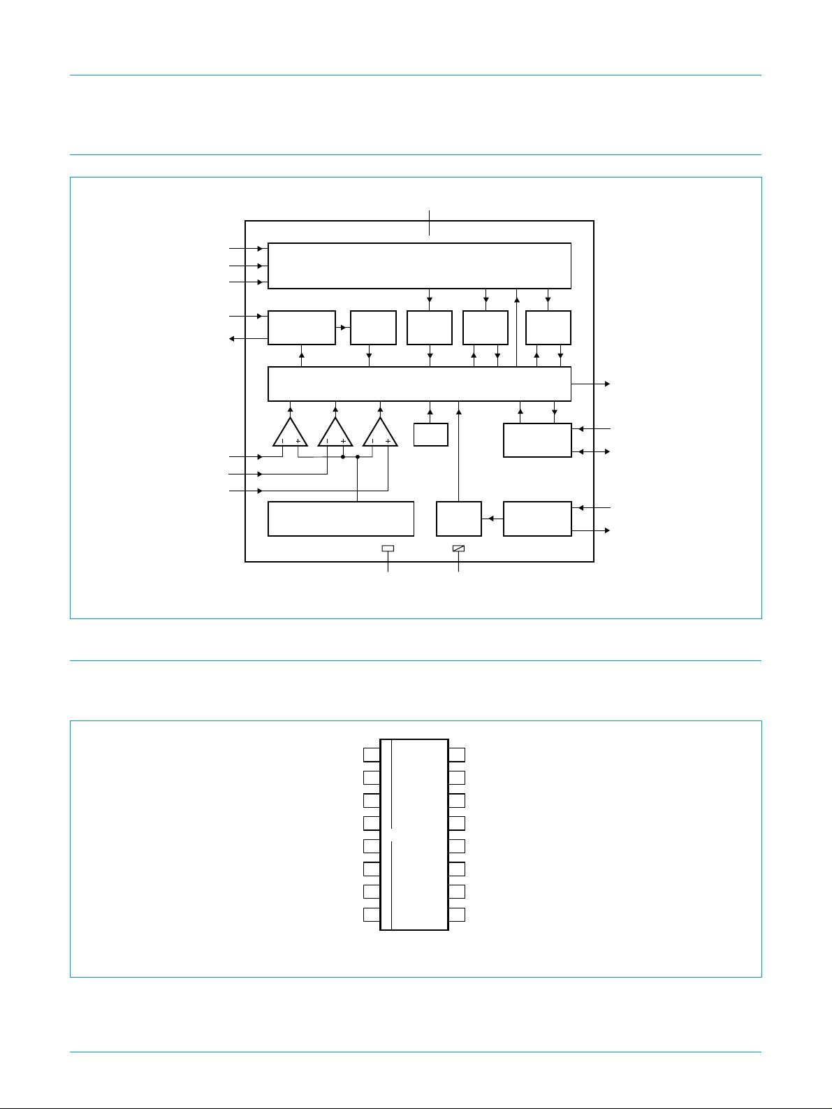
5. Block diagram
Unrestricted
handbook, full pagewidth
FSKIN+
FSKIN−
CASIN
15
14
13
V
DD
16
PREPROCESSOR
PCD3316
CIDCW receiver
HXIN
HXOUT
LOWBAT
POL0
POL1
1
2
OSCILLATOR
12
11
10
Fig 1. Block diagram.
6. Pinning information
6.1 Pinning
3.58 MHz
TIMING
VOLTAGE
REFERENCE
LEVEL
DETECT
CONTROL
POR
89
DGND
CAS
TIME
BASE
AGND
I2C-BUS
INTERFACE
PCD3316
32.768 kHz
OSCILLATOR
FSK
MBH983
3
IRQ
4
SCL
5
SDA
6
LXIN
7
LXOUT
handbook, halfpage
HXIN V
1
HXOUT FSKIN+
2
3
IRQ FSKIN−
SCL CASIN
4
PCD3316
5
SDA LOWBAT
LXIN POL0
6
LXOUT POL1
7
8
DGND AGND
MBH980
16
DD
15
14
13
12
11
10
9
Fig 2. Pin configuration.
9397 750 04824
Product specification 11 March 1999 3 of 30
© Philips Electronics N.V. 1999. All rights reserved.

Philips Semiconductors
6.2 Pin description
Table 2: Pin description
Symbol Pin I/O Description
Unrestricted
HXIN 1 I 3.58 MHz crystal oscillator input
HXOUT 2 O 3.58 MHz crystal oscillator output
IRQ 3 O interrupt output; programmable active HIGH or active LOW
SCL 4 I serial clock line of I
SDA 5 I/O serial data line of I
LXIN 6 I 32.768 kHz crystal oscillator input
LXOUT 7 O 32.768 kHz crystal oscillator output
DGND 8 − digital ground
AGND 9 − analog ground
POL1 10 I polarity detector input 1
POL0 11 I polarity detector input 0
LOWBAT 12 I low battery detector input
CASIN 13 I input pin for CAS signal
FSKIN− 14 I negative input for FSK signal
FSKIN+ 15 I positive input for FSK signal
V
DD
16 − supply
2
C-bus
2
C-bus
PCD3316
CIDCW receiver
7. Functional description
7.1 Preprocessor and analog inputs
The preprocessor for the CAS detection and the FSK receiver incorporates an
Analog-to-Digital Converter (ADC) and a digital bandpass filter.
The LOWBAT input of the PCD3316 can be used for low battery detection. The
voltage on the LOWBAT pin is compared with an internal voltage reference circuit.
When the LOWBAT voltage drops below the reference voltage, the Status register,
bit 5 is set to logic 1.
The PCD3316 can be forced in a Power-down state by switching off the 3.58 MHz
system clock and the ADC. This is done by setting Mode register 2, bit 7 (CIDMD2.7)
to logic 0. To guarantee correct operation the following order of actions must be
performed (see also Section 7.8 about interrupts):
1. Switch off CAS and FSK detection (if turned on)
2. Read the interrupt register (thus clearing pending interrupts generated by the
CAS and FSK detector)
3. Switch off the 3.58 MHz oscillator by clearing bit 7 of Mode register 2.
The two low power comparators (inputs POL0 and POL1) and the 32.768 kHz clock
are always active.
9397 750 04824
Product specification 11 March 1999 4 of 30
© Philips Electronics N.V. 1999. All rights reserved.

Philips Semiconductors
They can be used for ring or line polarity reversal detection. The POL on/off bit (Mode
register 1, bit 4) must be set to enable generation of an interrupt when a polarity
change occurs. The result of the two comparators can be read in bits 7 and 6 (POL0
and POL1) of the Status register (see Section 7.4). The 3.58 MHz clockis not needed
Unrestricted
for the generation of a polarity interrupt.
7.2 CAS detection
After a power-on reset or after enabling the CAS detector the internal registers of the
CAS detection function are initialized. The initialization takes a maximum of
100 periods of the 3.58 MHz clock.
If the CAS detection is enabled the PCD3316 will generate an interrupt (Interrupt
register, bit 1 is set) when a correct dual tone (2130 and 2750 Hz) is detected.
Interrupts will be blocked when the signal level on the CAS input is below the
threshold in the level detector.
7.3 FSK reception
The FSK receiver function can be enabled by setting the FSK on/off bit (Mode
register 1, bit 7).
PCD3316
CIDCW receiver
In the FSK transmission specification of BT and Bellcore a channel seizure is
transmitted first (sequence of 1010..). After the channel seizure a block of marks and
finally the data pattern are sent (see Figure 3). These mark bits are detected by the
PCD3316 which sets the FSK-BOM Indication bit (Status register, bit 4). The
FSK-BOM Indication bit is reset when the FSK receiver is disabled.
idth
channel seizure mark
FSK-BOM
Fig 3. FSK transmission specification.
If the FSK-BOM Indication bit is set, the FSK receiver will generate an interrupt after it
has received a complete data word. An FSK data word consists of one start bit
(space), followed by eight data bits and one stop bit (mark). Interrupts will therefore
not be generated during the channel seizure and during the block of marks. When a
valid data word has been received, FSK data is available in the FSK data register.
By clearing the FSK-BOM-mask on/off bit (Mode register 1, bit 6), the FSK receiver
will not wait with the generation of interrupts until a Begin Of Mark (BOM) has been
detected but will handle the channel seizure as normal data. The block of marks
which is a string of logic 1 will still not generate interrupts because there are no start
bits.
FSK transmission
data
MBH979
After the generation of an interrupt the IRQ pin will become active (see Figure 4), and
the FSK Interrupt bit is set (Interrupt register, bit 5). The received data is available in
the FSK data register.
9397 750 04824
Product specification 11 March 1999 5 of 30
© Philips Electronics N.V. 1999. All rights reserved.

Philips Semiconductors
PCD3316
CIDCW receiver
handbook, full pagewidth
Unrestricted
Fig 4. IRQ generation after reading a valid data byte.
IRQ
read by
serial interface
START
D0 D1 D2 D3 D4 D5 D6 D7 STOP
The FSK-OVR Error bit (Status register, bit 3) indicates that a previous byte is lost
due to an overrun. The FSK-FRM Error bit (Status register, bit 2) indicates an
incorrect start- or stop-bit. These frame errors indicate that there are synchronization
problems. The on-chip level detector can be used to detect a carrier loss during FSK
transmission. FSK data can be rejected when the signal level is below the reference
level, this to avoid that noise is interpreted as data (Interrupt register, bit 4 is logic 1).
7.4 Ring or polarity change detector
For ring and polarity change detection two comparators are available in the
PCD3316. The reference level of the comparators is set internally by the reference
voltage generator. The voltage levels on the two polarity comparator inputs, POL0
and POL1, are compared with the reference voltage V
POL1 > V
reset if POL0 > V
logic 1 to logic 0, a POL0 interrupt is generated. Every time the POL1 status bit
changes from logic 0 to logic 1, a POL1 interrupt is generated.
, POL0 and POL1 (Status register, bit 7 and 6) are set respectively and
ref
and POL1 < V
ref
MBH981
. If POL0 < V
ref
. Every time the POL0 status bit changes from
ref
ref
or
The period time of a POL1-POL0-POL1 sequence is available in the Ringer period
register. It is preset to 255 on power-on and updated every time a POL1 interrupt is
generated. The sequence is:
1. Power-on: Ringer period register = 255
2. First POL1 interrupt: Ringer period register = 255
3. First POL1 interrupt after a POL0 interrupt: Ringer period register = new time
4. First POL1 interrupt after more than
The period is given in multiples of1⁄
255
⁄
s: Ringer period register = 255.
2048
s. The maximum value is 255.
2048
The POL1-POL0-POL1 sequence is recognized when one or more POL1 interrupts
are generated followedbyone or more POL0 interrupts, followedbya POL1 interrupt.
The 32.768 kHz clock is needed for the generation of a polarity interrupt.
7.5 Low battery detection
The low battery voltage detection input (pin LOWBAT) is connected to the positive
input of a comparator. The negative input is connected to the internal reference
voltage.If the voltageon the LOWBAT input pin is less than the referencevoltage V
the LOW-BAT Indication (Status register, bit 5) is set. If the LOWBAT input rises
above V
9397 750 04824
Product specification 11 March 1999 6 of 30
again, the LOW-BAT Indication is cleared.
ref
© Philips Electronics N.V. 1999. All rights reserved.
ref
,

Philips Semiconductors
The 32.768 kHz clock signal must be available. The LOW-BAT Indication bit does not
generate interrupts, thus the bit should be polled.
7.6 Level detect
Unrestricted
When the input signal level on the FSK or the CAS input (the one that is selected) is
below a threshold of typically −40 dBm, the Low Level Status bit will be set (Interrupt
register, bit 4). The level detector can be used to observe a carrier loss during FSK
transmission and to detect the ‘Idle State Tone Alert Signal’ for British Telecom. The
signal power on the input can be monitored by polling the register bit since it will not
generate an interrupt. Signal power is measured in a frequency band corresponding
to the selected operation mode, FSK (1000 to 2200 Hz) or CAS (2000 to 2800 Hz).
The Low Level Status bit will be updated every 8 ms. When FSK and CAS are both
disabled the signal level on the FSK input is measured. The 32.768 kHz clock signal
must be available.
7.7 Time base
The 32.768 kHz oscillator is used to generate either a 1 second or a 1 minute
interrupt signal. If the TB on/off bit is set (Mode register 2, bit 6) every second or
minute an interrupt is generated and MIN Interrupt and/or SEC Interrupt bits
(Interrupt register, bit 7 and 6) are set. After reading the Interrupt register the interrupt
is cleared.
PCD3316
CIDCW receiver
The SEC/MIN (Mode register 2, bit 5) selects whether every second (SEC/MIN is set)
or every minute (SEC/MIN is cleared) an interrupt is generated. All possible
selections are shown in Table 3. Resetting bit TB on/off in Mode register 2 (bit 6) will
only disable time base interrupts, and the 32.768 kHz oscillator will continue to run.
7.8 Interrupt
The interrupt request output (IRQ) is active HIGH by default. The polarity of the IRQ
output can be made active LOW by the INT Polarity HIGH/LOW bit (Mode register 1,
bit 3). The IRQ pin is in 3-state when not active, so an external pull-up or pull-down
resistor is required. The interrupt cause is indicated by the flags in the Interrupt
register.Interrupt flags are set by hardware but must be reset by software. All flags of
the Interrupt register are reset when the register is read via I2C-bus interface.
The IRQ pin is deactivated at the positive edge of SCL which reads the first data bit of
the Interrupt register. The IRQ pin will stay inactive for one SCL cycle. IRQ can
handle a next interrupt after the next positive edge of SCL.
Table 3: Selection of interrupt modes
Mode register 2 (CIDMD2) Interrupt register (CIDINT) Interrupt
TB on/off
(CIDMD2.6)
0X
1 0 1 0 every minute an interrupt is generated; no second interrupt
1 1 1 1 every second an interrupt is generated; every minute an
SEC/MIN
(CIDMD2.5)
[1]
MIN Interrupt
(CIDINT.7)
0 0 no time base interrupt (time base is reset)
SECInterrupt
(CIDINT.6)
interrupt is generated
[1] X = don’t care.
9397 750 04824
Product specification 11 March 1999 7 of 30
© Philips Electronics N.V. 1999. All rights reserved.
Philips Semiconductors
7.9 The internal Power-on reset (POR)
The device contains an on-chip Power-on reset circuitry which activates a reset as
long as VDD is below a predefined level V
Unrestricted
3.58 MHz oscillator will start. The PCD3316 is initialized and the internal registers are
set to the default value (see Section 7.13). It takes a maximum of 100 cycles of the
3.58 MHz clock to initialize all internal functions. The POR circuitry also ensures, that
the chip will be switched off as soon as a falling VDD reaches a predefined level
(V
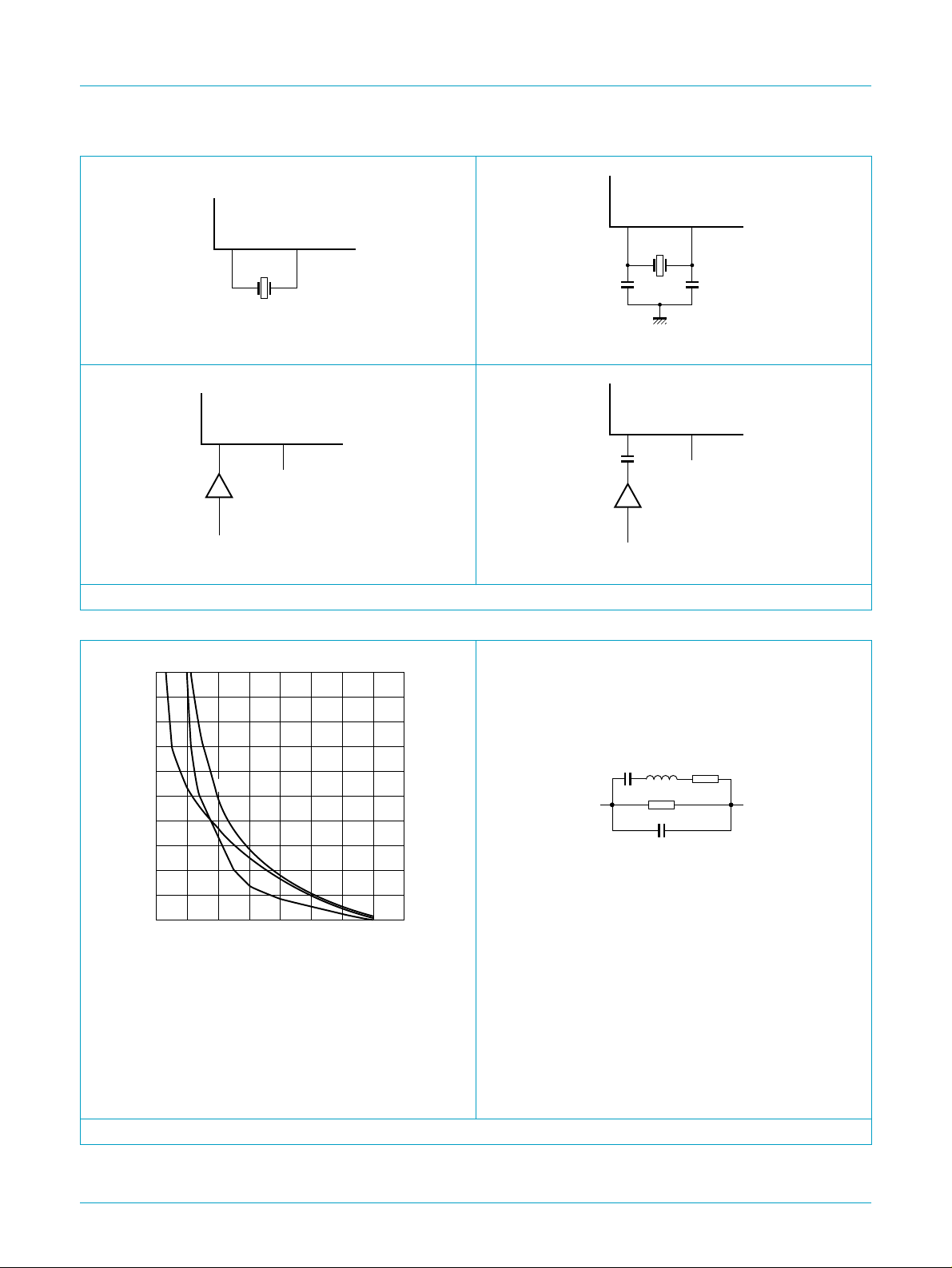
7.10 3.58 MHz oscillator circuitry
The 3.58 MHz oscillator is needed for the FSK receiver and the CAS detection. This
on-chip Amplitude Controlled Oscillator (ACO) circuitry is a single-stage inverting
amplifier biased by an internal feedback resistor Rfb. The oscillator circuit is shown in
Figure 5. When using a quartz resonator to drive the oscillator, normally no external
components are needed.
When using ceramic resonators to drive the oscillator, in some cases external
components are needed; refer to the ceramic resonator product specifications. Two
different configurations are shown in Figure 6a and Figure 6b.
POR(L)
PCD3316
CIDCW receiver
. If VDD exceeds V
POR(H)
).
POR(H)
, the
handbook, halfpage
Fig 5. Oscillator.
AMPLITUDE
CONTROL
PCD3316
R
fb
C1
i
12
C1
e
on/off
C2
i
HXOUTHXIN
C2
e
MGK723
To drive the device with an external clock source, apply the external clock signal to
HXIN, and leave HXOUT to float, as shown in Figure 6c. If the amplitude of the input
signal is less than VDD to DGND or a sine wave is applied, capacitive decoupling is
needed as shown in Figure 6d.
In the Power-down mode (Mode register 2, bit 7 = 0), the oscillator is stopped and
HXIN and HXOUT are internally pulled LOW. The current of the whole oscillator is
switched off.
9397 750 04824
Product specification 11 March 1999 8 of 30
© Philips Electronics N.V. 1999. All rights reserved.
Philips Semiconductors
PCD3316
CIDCW receiver
handbook, halfpage
Unrestricted
PCD3316
1
HXIN
2
HXOUT
MGK725
handbook, halfpage
C1
e
1
HXIN
PCD3316
2
HXOUT
C2
e
MGK726
a. Standard oscillator: quartz or PXE. b. Oscillator: quartz or PXE with external capacitors.
handbook, halfpage
PCD3316
1
HXIN
3.58 MHz
square wave
handbook, halfpage
2
HXOUT
MGK727
PCD3316
1
HXIN
3.58 MHz
sine wave
2
HXOUT
MGK728
c. External clock: square wave. d. External clock: sine wave.
Fig 6. 3.58 MHz oscillator configurations.
60
MBK948
C0 (pF)
C1
handbook, halfpage
L1
R0
C0
For correct function of the oscillator, the values
of R1 and C0 of the chosen resonator (quartz or
PXE) must be below the related curve lines
shown in Figure 7a. The value of the parallel
resistor R0 must be less than 47 kΩ.
The wiring between chip and resonator should
be kept as short as possible.
500
handbook, halfpage
R1
(Ω)
400
300
200
100
0
0
(3)
(2)
(1)
20 40 80
C1eand C2e are the external load capacitances
(see Figure 6b). Normally, they are not needed
due to integrated load capacitances of 10 pF;
see curve (2).
(1) C1e=C2e=22pF.
(2) C1e=C2e= 0 pF.
(3) C1e=C2e=12pF.
a. Resonator requirements for the ACO. b. Resonator equivalent circuit.
Fig 7. Resonator requirements and equivalent circuit.
R1
MBK947
9397 750 04824
© Philips Electronics N.V. 1999. All rights reserved.
Product specification 11 March 1999 9 of 30
 Loading...