

Philips PCD3311CP, PCD3311CT, PCD3312CP, PCD3312CT Datasheet

INTEGRATED CIRCUITS
DATA SH EET
PCD3311C; PCD3312C
DTMF/modem/musical-tone
generators
Product specification
Supersedes data of May 1990
File under Integrated Circuits, IC03
1996 Nov 21

Philips Semiconductors Product specification
DTMF/modem/musical-tone generators PCD3311C; PCD3312C
CONTENTS
1 FEATURES
2 GENERAL DESCRIPTION
3 QUICK REFERENCE DATA
4 ORDERING INFORMATION
5 BLOCK DIAGRAM
6 PINNING INFORMATION
6.1 Pinning PCD3311CP
6.2 Pin description PCD3311CP
6.3 Pinning PCD3311CT
6.4 Pin description PCD3311CT
6.5 Pinning PCD3312C
6.6 Pin description PCD3312C
7 FUNCTIONAL DESCRIPTION
7.1 General
7.2 Clock/oscillator connection
7.3 Mode selection (PCD3311C)
7.4 Data inputs (PCD3311C)
7.5 Strobe input (PCD3311C )
7.6 I2C-bus clock and data inputs
7.7 Address input
7.8 I2C-bus data configuration
7.9 Tone output
7.10 Power-on reset
7.11 Tables of Input and output
8I
8.1 Bit transfer
8.2 Start and stop conditions
8.3 System configuration
8.4 Acknowledge
8.5 Timing specifications
8.5.1 Standard mode
8.5.2 Low-speed mode
9 HANDLING
10 LIMITING VALUES
11 CHARACTERISTICS
12 APPLICATION INFORMATION
13 PACKAGE OUTLINES
14 SOLDERING
14.1 Introduction
14.2 DIP
14.2.1 Soldering by dipping or by wave
14.2.2 Repairing soldered joints
14.3 SO
14.3.1 Reflow soldering
14.3.2 Wave soldering
14.3.3 Repairing soldered joints
2
C-BUS INTERFACE
15 DEFINITIONS
16 LIFE SUPPORT APPLICATIONS
17 PURCHASE OF PHILIPS I2C COMPONENTS
1996 Nov 21 2
Philips Semiconductors Product specification
DTMF/modem/musical-tone generators PCD3311C; PCD3312C
1 FEATURES
• DTMF, modem and musical tone generation
• Stabilized output voltage level
• Low output distortion with on-chip filtering conforming to
CEPT recommendations
• Latched inputs for data bus applications
• I2C-bus compatible
• Selection of parallel or serial (I2C-bus) data input
(PCD3311C).
used, and a separate microcontroller is required to control
the devices.
Both the devices can interface to I
2
C-bus compatible
microcontrollers for serial input. The PCD3311C can also
interface directly to all standard microcontrollers,
accepting a binary coded parallel input.
With their on-chip voltage reference the PCD3311C and
PCD3312C provide constant output amplitudes which are
independent of the operating supply voltage and ambient
temperature.
An on-chip filtering system assures a very low total
2 GENERAL DESCRIPTION
The PCD3311C and PCD3312C are single-chip silicon
gate CMOS integrated circuits. They are intended
principally for use in telephone sets to provide the
dual-tone multi-frequency (DTMF) combinations required
for tone dialling systems. The various audio output
frequencies are generated from an on-chip 3.58 MHz
quartz crystal-controlled oscillator. A separate crystal is
harmonic distortion in accordance with CEPT
recommendations.
In addition to the standard DTMF frequencies the devices
can also provide:
• Twelve standard frequencies used in simplex modem
applications for data rates from 300 to 1200 bits per
second
• Two octaves of musical scales in steps of semitones.
3 QUICK REFERENCE DATA
SYMBOL PARAMETER MIN. TYP. MAX. UNIT
V
DD
I
DD
I
stb
V
HG(RMS)
V
LG(RMS)
G
v
operating supply voltage 2.5 − 6.0 V
operating supply current −−0.9 mA
standby current −−3µA
DTMF HIGH group output voltage level (RMS value) 158 192 205 mV
DTMF LOW group output voltage level (RMS value) 125 150 160 mV
pre-emphasis (voltage gain) of group 1.85 2.10 2.35 dB
THD total harmonic distortion −−25 − dB
T
amb
operating ambient temperature −25 − +70 °C
4 ORDERING INFORMATION
PACKAGE
TYPE NUMBER
NAME DESCRIPTION VERSION
PCD3311CP DIP14 plastic dual in-line package; 14 leads (300 mil) SOT27-1
PCD3311CT SO16 plastic small outline package; 16 leads; body width 7.5 mm SOT162-1
PCD3312CP DIP8 plastic dual in-line package; 8 leads (300 mil) SOT97-1
PCD3312CT SO8 plastic small outline package; 8 leads; body width 7.5 mm SOT176-1
1996 Nov 21 3

Philips Semiconductors Product specification
DTMF/modem/musical-tone generators PCD3311C; PCD3312C
5 BLOCK DIAGRAM
handbook, full pagewidth
D5
D4
D3
D2
3
4
12
11
10
9(8)
8(7)
5
MODE
D1/SDA
D0/SCL
STROBE
The un-parenthesised numbers are for the PCD3311CP, those in parenthesis for the PCD3312C.
OSCI OSCO
OSCILLATOR
INPUT
CONTROL
LOGIC
A
0
1(3)
7(6)
2(4)
GENERATOR
HIGH
GROUP
DIVIDER
DIVIDER
SELECTION
(ROM)
LOW
GROUP
DIVIDER
CLOCK
SWITCHED
CAPACITOR
BANDGAP
VOLTAGE
REFERENCE
ADDER
Fig.1 Block diagram.
DAC
HIGH
DAC
LOW
V
DD
14(2) 13(1)
SWITCHED
CAPACITOR
PCD3311C
PCD3312C
V
SS
RESISTOR
CAPACITOR
MGG543
(5)6
TONE
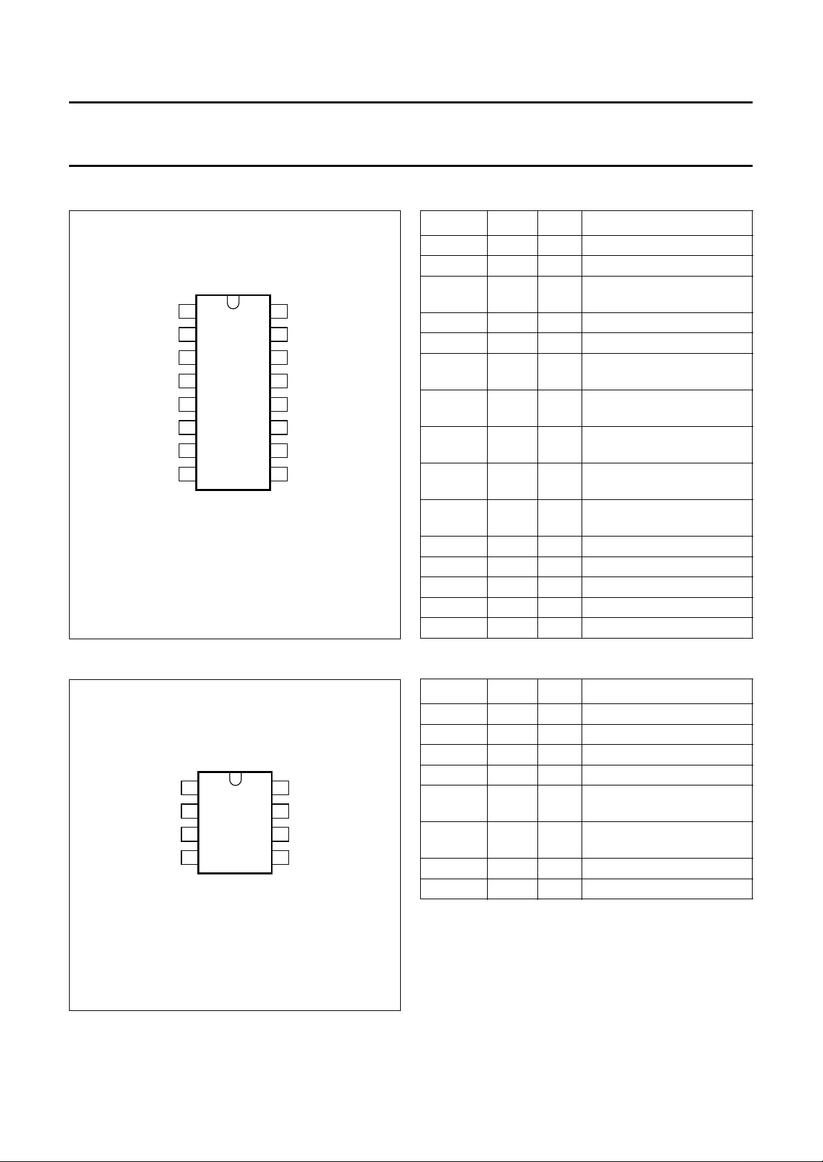
6 PINNING INFORMATION
6.1 Pinning PCD3311CP
handbook, halfpage
OSCI
OSCO
MODE
D5
STROBE
TONE
A0
1
2
3
4
PCD3311CP
5
6
7
Fig.2 Pin configuration PCD3311CP.
MGG508
14
13
12
11
10
9
8
V
DD
V
SS
D4
D3
D2
D1/SDA
D0/SCL
6.2 Pin description PCD3311CP
SYMBOL PIN TYPE DESCRIPTION
OSCI 1 I oscillator input
OSCO 2 O oscillator output
MODE 3 I mode select input (selects
2
C or parallel data input)
I
D5 4 I parallel data input
STROBE 5 I strobe input (for loading
data in parallel mode)
TONE 6 O frequency output (DTMF,
modem, musical tones)
A0 7 I slave address input (to be
connected to V
or VSS)
DD
D0/SCL 8 I parallel data input or
2
C-bus clock line
I
D1/SDA 9 I parallel data input or
2
C-bus data line
I
D2 − D4 10 − 12 I parallel data inputs
V
SS
V
DD
13 P negative supply
14 P positive supply
1996 Nov 21 4
Philips Semiconductors Product specification
DTMF/modem/musical-tone generators PCD3311C; PCD3312C
6.3 Pinning PCD3311CT
handbook, halfpage
OSCI
OSCO
MODE
D5
n.c.
STROBE
TONE
A0
1
2
3
4
PCD3311CT
5
6
7
8
Fig.3 Pin configuration PCD3311CT.
MGG509
16
15
14
13
12
11
10
9
V
DD
V
SS
D4
n.c.
D3
D2
D1/SDA
D0/SCL
6.4 Pin description PCD3311CT
SYMBOL PIN TYPE DESCRIPTION
OSCI 1 I oscillator input
OSCO 2 O oscillator output
MODE 3 I mode select input (selects
2
C or parallel data input)
I
D5 4 I parallel data input
n.c. 5 − not connected
STROBE 6 I strobe input (for loading
data in parallel mode)
TONE 7 O frequency output (DTMF,
modem, musical tones)
A0 8 I slave address input (to be
connected to V
or VSS)
DD
D0/SCL 9 I parallel data input or
2
C-bus clock line
I
D1/SDA 10 I parallel data input or
2
C-bus data line
I
D2, D3 11, 12 I parallel data inputs
n.c. 13 − not connected
D4 14 I parallel data input
V
SS
V
DD
15 P negative supply
16 P positive supply
6.5 Pinning PCD3312C
handbook, halfpage
V
SS
V
DD
OSCI
OSCO
1
2
PCD3312C
3
4
Fig.4 Pin configuration PCD3312C.
MGG510
6.6 Pin description PCD3312C
SYMBOL PIN TYPE DESCRIPTION
V
SS
V
DD
1 P negative supply
2 P positive supply
OSCI 3 I oscillator input
OSCO 4 O oscillator output
SDA
8
SCL
7
A0
6
TONE
5
TONE 5 O frequency output (DTMF,
modem, musical tones)
A0 6 I slave address input (to be
or VSS)
DD
SCL 7 I I
SDA 8 I I
connected to V
2
C-bus clock line
2
C-bus data line
1996 Nov 21 5
Philips Semiconductors Product specification
DTMF/modem/musical-tone generators PCD3311C; PCD3312C
7 FUNCTIONAL DESCRIPTION
7.1 General (see Fig.1)
The Input Control Logic decodes the input data to
determine whether DTMF, modem or musical tones are
selected; and which particular tone or combination of
tones is required.
A code representing the required tones is sent to the
Divider Selection ROM which selects the correct division
ratio in both of the Frequency Dividers (or in one divider, if
only a single tone is required).
The Oscillator circuit provides a square wave of frequency
3.58 MHz. Each Frequency Divider divides the frequency
of the Oscillator to give a serial digital square wave with a
frequency simply related to that of the required tone.
The output from each Frequency Divider goes to a DAC,
which is also fed by a clock derived from the oscillator.
Using these two signals, the DAC produces an
approximate sine wave of the required frequency, with an
amplitude derived from the Voltage Reference.
The output from the DAC goes to an Adder where, for
DTMF, it is combined with the output from the other DAC.
The output from the Adder goes through two stages of Low
Pass Filters to give a smoothed tone (single or dual), and
finally to the TONE output.
7.4 Data inputs (PCD3311C)
Inputs D0, D1, D2, D3, D4 and D5 are used in the parallel
data input mode of the PCD3311C. Inputs D0 and D1 are
also used in serial input mode when they act as the SCL
and SDA inputs respectively. Inputs D0 and D1 have no
internal pull-down or pull-up resistors and must not be left
open in any application. Inputs D2, D3, D4 and D5 have
internal pull-down.
D4 and D5 are used to select between DTMF dual, DTMF
single, modem and musical tones (see Table 1). D0, D1,
D2 and D3 select the tone combination or single tone
within the selected application. They also, in combination
with D4, select the standby mode. See Tables 2, 3, 4
and 5.
PCD 3312C has no parallel data pins as data input is via
2
C-bus.
the I
Table 1 Use of D5 and D4 to select application
D5 D4 APPLICATION
LOW LOW DTMF single tones; musical tones;
standby
LOW HIGH DTMF dual tones (all 16 combinations)
HIGH LOW modem tones
HIGH HIGH musical tones
7.2 Clock/oscillator connection
The timebase for the PCD3311C and PCD3312C is a
crystal-controlled oscillator, requiring a 3.58 MHz quartz
crystal to be connected between OSCI and OSCO.
Alternatively, the OSCI input can be driven from an
external clock of 3.58 MHz.
7.3 Mode selection (PCD3311C)
The MODE input selects the data input mode for the
PCD3311C. When MODE is connected to V
(HIGH),
DD
data can be received in the parallel mode. When
connected to VSS (LOW) or left open, data can be received
via the serial I2C-bus.
PCD 3312C has no MODE input as data input is via the
I2C-bus only.
7.5 Strobe input (PCD3311C )
The STROBE input (with internal pull-down) allows the
loading of parallel data into D0 to D5 when MODE is HIGH.
The data inputs must be stable preceding the
positive-going edge of the strobe pulse (active HIGH).
Input data are loaded at the negative-going edge of the
strobe pulse and then the corresponding tone (or standby
mode) is provided at the TONE output. The output remains
unchanged until the negative-going edge of the next
STROBE pulse (for new data) is received. Figure 5 is an
example of the timing relationship between STROBE and
the data inputs.
When MODE is LOW, data is received serially via the
2
C-bus.
I
1996 Nov 21 6

Philips Semiconductors Product specification
DTMF/modem/musical-tone generators PCD3311C; PCD3312C
90%
t
SPW
t
DH
oscillator OFF
t
(ON)
tone
oscillator ON
no output tone
oscillator ON
output tones
handbook, full pagewidth
STROBE
TONE
10%
t
DS
D0
D1
D2
D3
D4
D5
MGG511
Fig.5 Timing of STROBE, parallel data inputs and TONE output (770 Hz + 1477 Hz in example) in the parallel
mode (MODE = HIGH).
7.6 I2C-bus clock and data inputs
SCL and SDA are the serial clock and serial data inputs
according to the I2C-bus specification, see Chapter 8.
SCL and SDA must be pulled up externally to VDD.
For the PCD3311C, SCL and SDA are combined with
parallel inputs D0 and D1 respectively - D0/SCL and
D1/SDA operate serially only when MODE is LOW.
7.7 Address input
Address input A0 defines the least significant bit of the
2
C-bus address of the device (see Fig.6). The first 6 bits
I
of the address are fixed internally. By tying the A0 of each
device to VDD (HIGH) and VSS(LOW) respectively, two
different PCD3311C or PCD3312C devices can be
individually addressed on the bus.
Whether one or two devices are used, A0 must be
connected to VDD or VSS.
1996 Nov 21 7
7.8 I
2
C-bus data configuration (see Fig.6)
The PCD3311C and PCD3312C are always slave
receivers in the I2C-bus configuration. The R/W bit in is
thus always LOW, indicating that the master
(microcontroller) is writing.
The slave address in the serial mode consists of 7 bits: 6
bits internally fixed, 1 externally set via A0. in the serial
mode, the same input data codes are used as in the
parallel mode. See Tables 2, 3, 4 and 5.
7.9 Tone output
The single and dual tones provided at the TONE output are
first filtered by an on-chip switched-capacitor filter,
followed by an active RC low-pass filter. The filtered tones
fulfil the CEPT recommendations for total harmonic
distortion of DTMF tones. An on-chip reference voltage
provides output tone levels independent of the supply
voltage. Tables 3, 4 and 5 give the frequency deviation of
the output tones with respect to the standard DTMF,
modem and music frequencies.

Philips Semiconductors Product specification
DTMF/modem/musical-tone generators PCD3311C; PCD3312C
handbook, full pagewidth
acknowledge
from slave
MSB
S 010010A00AXXD5D4D3D2D1D0AP
slave address data
MGG512
R/W
acknowledge
from slave
internal STROBE
for data latching
Fig.6 I2C-bus data format.
7.10 Power-on reset
In order to avoid an undefined state when the power is switched ON, the devices have an internal reset circuit which sets
the standby mode (oscillator OFF).
7.11 TABLES OF INPUT AND OUTPUT
The specified output tones are obtained when a 3.579545 MHz crystal is used.
In each table, the logical states for the input data lines are related to voltage levels as follows:
1 = HIGH = V
0 = LOW = V
DD
SS
X = don’t care
Table 2 Input data for no output tone, TONE in 3-state
D5 D4 D3 D2 D1 D0 HEX
(1)
X 0 0 0 0 0 00 or 20 ON
X 0 0 0 0 1 01 or 21 OFF
X 0 0 0 1 0 02 or 22 OFF
X 0 0 0 1 1 03 or 23 OFF
Note
1. The alternative HEX values depend on the value of D5.
1996 Nov 21 8
OSCILLATOR

Philips Semiconductors Product specification
DTMF/modem/musical-tone generators PCD3311C; PCD3312C
Table 3 Input data and output for DTMF tones
STANDARD
D5 D4 D3 D2 D1 D0 HEX SYMBOL
00100008 − 697 697.90 +0.13 +0.90
00100109 − 770 770.46 +0.06 +0.46
0010100A − 852 850.45 −0.18 −1.55
0010110B − 941 943.23 +0.24 +2.23
0011000C − 1209 1206.45 −0.21 −2.55
0011010D − 1336 1341.66 +0.42 +5.66
0011100E − 1477 1482.21 +0.35 +5.21
0011110F − 1633 1638.24 +0.32 +5.24
01000010 0 941+1336 −−−
01000111 1 697+1209 −−−
01001012 2 697+1336 −−−
01001113 3 697+1477 −−−
01010014 4 770+1209 −−−
01010115 5 770+1336 −−−
01011016 6 770+1477 −−−
01011117 7 852+1209 −−−
01100018 8 852+1336 −−−
01100119 9 852+1477 −−−
0110101A A697+1633 −−−
0110111B B770+1633 −−−
0111001C C852+1633 −−−
0111011D D941+1633 −−−
0111101E * 941+1209 −−−
0111111F # 941+1477 −−−
FREQUENCY
Hz Hz % Hz
TONE
OUTPUT
FREQ.
FREQUENCY
DEVIATION
Table 4 Input data and output for modem tones
STANDARD
D5 D4 D3 D2 D1 D0 HEX
10010024 13001296.94 −0.24 −3.06
10010125 21002103.14 +0.15 +3.14
10011026 12001197.17 −0.24 −2.83
10011127 22002192.01 −0.36 −7.99
10100028 980978.82 −0.12 −1.18
10100129 11801179.03 −0.08 −0.97
1996 Nov 21 9
FREQUENCY
Hz Hz % Hz
TONE
OUTPUT
FREQ.
FREQUENCY
DEVIATION
TELECOM.
STANDARD
V.23
Bell 202
V.21
 Loading...