

Philips PCA82C251U, PCA82C251, PCA82C251T Datasheet

INTEGRATED CIRCUITS
DATA SH EET
PCA82C251
CAN transceiver for 24 V systems
Product specification
Supersedes data of 1997 Mar 14
File under Integrated Circuits, IC18
2000 Jan 13

Philips Semiconductors Productspecification
CAN transceiver for 24 V systems PCA82C251
FEATURES
• Fully compatible with the
“ISO 11898-24 V”
standard
• Slope control to reduce RFI
• Thermally protected
• Short-circuit proof to battery and ground in 24 V
powered systems
GENERAL DESCRIPTION
The PCA82C251 is the interface between the CAN
protocol controller and the physical bus. It is primarily
intended for applications (up to 1 Mbaud) in trucks and
buses. The device provides differentialtransmit capability
to the bus and differential receive capability to the CAN
controller.
• Low-current standby mode
• An unpowered node does not disturb the bus lines
• At least 110 nodes can be connected
• High speed (up to 1 Mbaud)
• High immunity against electromagnetic interference.
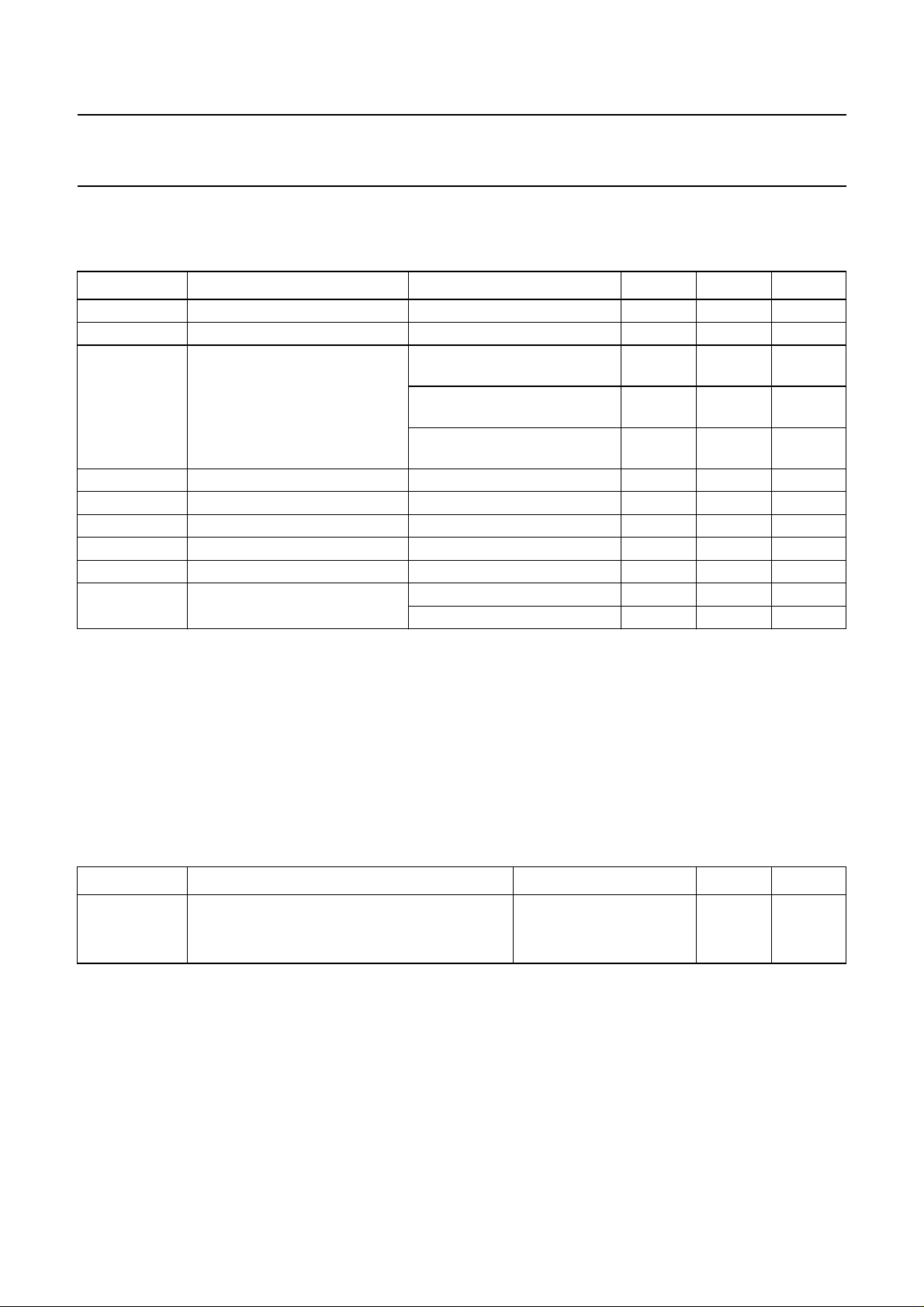
QUICK REFERENCE DATA
SYMBOL PARAMETER CONDITIONS MIN. MAX. UNIT
V
I
1/t
V
V
T
CC
CC
bit
CAN
diff
amb
supply voltage 4.5 5.5 V
supply current standby mode − 275 µA
maximum transmission speed non-return-to-zero 1 − Mbaud
CANH, CANL input/output voltage −36 +36 V
differential bus voltage 1.5 3.0 V
ambient temperature −40 +125 °C
ORDERING INFORMATION
TYPE
NUMBER
NAME DESCRIPTION CODE
PACKAGE
PCA82C251 DIP8 plastic dual in-line package; 8 leads (300 mil) SOT97-1
PCA82C251T SO8 plastic small outline package; 8 leads body width 3.9 mm SOT96-1
PCA82C251U − bare die; 2840 × 1780 × 380 µm −
2000 Jan 13 2

Philips Semiconductors Productspecification
CAN transceiver for 24 V systems PCA82C251
BLOCK DIAGRAM
handbook, full pagewidth
PINNING
TXD
Rs
RXD
V
ref
1
8
4
5
REFERENCE
SLOPE/
STANDBY
VOLTAGE
Fig.1 Block diagram.
PROTECTION
RECEIVER
PCA82C251
DRIVER
V
CC
GND
3
7
CANH
CANL
6
2
MBG613
SYMBOL PIN DESCRIPTION
TXD 1 transmit data input
GND 2 ground
V
CC
3 supply voltage
RXD 4 receive data output
V
ref
5 reference voltage output
CANL 6 LOW-level CAN voltage
input/output
CANH 7 HIGH-level CAN voltage
input/output
Rs 8 slope resistor input
2000 Jan 13 3
handbook, halfpage
1TXD
2
GND CANH
V
RXD
CC
PCA82C251
3
4
MBG612
8Rs
7
6
CANL
V
5
ref
Fig.2 Pin configuration.

Philips Semiconductors Productspecification
CAN transceiver for 24 V systems PCA82C251
FUNCTIONAL DESCRIPTION
The PCA82C251 is the interface between the CAN
protocol controller and the physical bus. It is primarily
intended for applications up to 1 Mbaud in trucks and
buses. The device provides differential transmit capability
to the bus and differential receive capability to the CAN
controller. It is fully compatible with the
“ISO 11898-24 V”
standard.
A current limiting circuit protects the transmitter output
stage against short-circuit to positive and negative battery
voltage. Although the power dissipation is increased
during this fault condition, this feature will prevent
destruction of the transmitter output stage.
If the junction temperature exceeds a value of
approximately 160 °C, the limiting current of both
transmitter outputs is decreased. Because the transmitter
is responsible for the major part of the power dissipation,
this will result in a reduced power dissipation and hence a
lowerchip temperature. All other partsof the IC will remain
operating. The thermal protection is particularly needed
when a bus line is short-circuited.
The CANH and CANL lines are also protected against
electrical transients which may occur in an automotive
environment.
Pin 8 (Rs) allows three different modes of operation to be
selected: high-speed, slope control or standby.
For high-speed operation, the transmitter output
transistors are simply switched on and off as fast as
possible. In this mode, no measures are taken to limit the
rise and fall slope. Use of a shielded cable is
recommended to avoid RFI problems. The high-speed
mode is selected by connecting pin 8 to ground.
The slope control mode allows the use of an unshielded
twisted pair or a parallel pair of wires as bus lines.
To reduce RFI, the rise and fall slope should be limited.
The rise and fall slope can be programmed with a resistor
connected from pin 8 to ground. The slope is proportional
to the current output at pin 8.
If a HIGH level is applied to pin 8, the circuit enters a low
current standby mode. In this mode, the transmitter is
switched off and the receiver is switched to a low current.
If dominant bits are detected (differential bus voltage
>0.9 V), RXD will be switched to a LOW level.
The microcontroller should react to this condition by
switching the transceiver back to normal operation
(via pin 8). Because the receiver is slower in standby
mode, the first message will be lost at higher bit rates.
Table 1 Truth table of the CAN transceiver
V
CC
TXD CANH CANL BUS STATE RXD
4.5 to 5.5 V 0 HIGH LOW dominant 0
4.5 to 5.5 V 1 (or floating) floating floating recessive 1
4.5<VCC< 5.5 V X
(1)
floating if
VRs> 0.75V
CC
floating if
VRs> 0.75V
floating 1
CC
0<VCC< 4.5 V floating floating floating floating X
Notes
1. X = don’t care.
2. If another bus node is transmitting a dominant bit, then RXD is logic 0.
Table 2 Pin Rs summary
CONDITION FORCED AT PIN Rs MODE RESULTING VOLTAGE OR CURRENT AT PIN Rs
> 0.75V
V
Rs
10 µA<−I
VRs< 0.3V
CC
< 200 µA slope control 0.4VCC<VRs< 0.6V
Rs
CC
standby −IRs<10µA
CC
high-speed −IRs< 500 µA
(2)
(2)
(1)
2000 Jan 13 4
Philips Semiconductors Productspecification
CAN transceiver for 24 V systems PCA82C251
LIMITING VALUES
In accordance with the Absolute Maximum Rating System (IEC 60134); all voltages are referenced to pin 2;
positive input current.
SYMBOL PARAMETER CONDITIONS MIN. MAX. UNIT
V
CC
V
n
V
6
V
7
V
tr
T
stg
T
amb
T
vj
V
esd
supply voltage −0.3 +7.0 V
DC voltage at pins 1, 4, 5 and 8 −0.3 VCC+ 0.3 V
DC voltage at pin 6 (CANL) 0V<VCC< 5.5 V; TXD HIGH
−36 +36 V
or floating
0V<V
< 5.5 V; no time
CC
−36 +36 V
limit; note 1
0V<V
< 5.5 V; no time
CC
−36 +36 V
limit; note 2
DC voltage at pin 7 (CANH) 0V<VCC< 5.5 V; no time limit −36 +36 V
transient voltage on pins 6 and 7 see Fig.8 −200 +200 V
storage temperature −55 +150 °C
ambient temperature −40 +125 °C
virtual junction temperature note 3 −40 +150 °C
electrostatic discharge voltage note 4 −2500 +2500 V
note 5 −250 +250 V
Notes
1. TXD is LOW. Short-circuit protection provided for slew rates up to 5 V/µs for voltages above +30 V.
2. Short-circuit applied when TXD is HIGH, followed by TXD switched to LOW.
3. In accordance with
Tvj=T
amb+Pd×Rth(vj-a)
“IEC 60747-1”
, where R
the allowable combinations of power dissipation (Pd) and ambient temperature (T
. An alternative definition of virtual junction temperature is:
is a fixed value to be used for the calculation of Tvj. The rating for Tvj limits
th(vj-a)
).
amb
4. Classification A: human body model; C = 100 pF; R = 1500 Ω; V = ±2500 V.
5. Classification B: machine model; C = 200 pF; R = 0 Ω; V = ±250 V.
THERMAL CHARACTERISTICS
SYMBOL PARAMETER CONDITIONS VALUE UNIT
R
th(j-a)
thermal resistance from junction to ambient in free air
PCA82C251 100 K/W
PCA82C251T 160 K/W
QUALITY SPECIFICATION
According to
“SNW-FQ-611 part E”
.
2000 Jan 13 5
Philips Semiconductors Productspecification
CAN transceiver for 24 V systems PCA82C251
CHARACTERISTICS
VCC= 4.5 to 5.5 V; T
to ground (pin 2); positive input current; all parameters are guaranteed over the ambient temperature range by design,
but only 100% tested at +25 °C.
SYMBOL PARAMETER CONDITIONS MIN. TYP. MAX. UNIT
Supply
I
3
supply current dominant; V1=1V;
DC bus transmitter
V
IH
V
IL
I
IH
I
IL
V
6, 7
I
LO
HIGH-level input voltage output recessive 0.7V
LOW-level input voltage output dominant −0.3 − 0.3V
HIGH-level input current V1=4V −200 − +30 µA
LOW-level input current V1=1V −100 −−600 µA
recessive bus voltage V1= 4 V; no load 2.0 − 3.0 V
off-state output leakage
current
V
V
∆V
7
6
6,7
CANH output voltage V1=1V; VCC= 4.75 to 5.5 V 3.0 − 4.5 V
CANL output voltage V1=1V 0.5 − 2.0 V
difference between output
voltage at pins 6 and 7
I
I
sc7
sc6
short-circuit CANH current V7= −5V −−−200 mA
short-circuit CANL current V6=36V −−200 mA
DC bus receiver [V1= 4 V; pins 6 and 7 externally driven; −2V<(V6,V7) < 7 V; unless otherwise specified]
= −40 to + 125 °C; RL=60Ω; I8> −10 µA; unless otherwise specified; all voltages referenced
amb
−−78 mA
VCC< 5.1 V
dominant; V
=1V;
1
−−80 mA
VCC< 5.25 V
dominant; V
=1V;
1
−−85 mA
VCC< 5.5 V
recessive; V
=4V;
1
−−10 mA
R8=47kΩ
standby; note 1 −−275 µA
− VCC+ 0.3 V
CC
CC
−2V<(V6,V7)<7V −2 − +2 mA
−5V<(V
=1V; VCC= 4.5 to 4.75 V 2.75 − 4.5 V
V
1
) < 36 V −10 − +10 mA
6,V7
V1=1V 1.5 − 3.0 V
V
=1V; RL=45Ω 1.5 −−V
1
V
= 4 V; no load −500 − +50 mV
1
V
= −36 V −−100 − mA
7
V
V
V
diff(r)
diff(d)
differential input voltage
(recessive)
differential input voltage
(dominant)
note 2 −1.0 − +0.5 V
−7V<(V
−7V<(V
) < 12 V; note 2 −1.0 − +0.4 V
6,V7
) < 12 V; not
6, V7
standby mode
standby mode 0.97 − 5.0 V
standby mode;
V
= 4.5 to 5.10 V
CC
V
diff(hys)
differential input hysteresis see Fig.5 − 150 − mV
2000 Jan 13 6
0.9 − 5.0 V
1.0 − 5.0 V
0.91 − 5.0 V
 Loading...