

Philips PCA5010H Datasheet

INTEGRATED CIRCUITS
DATA SH EET
PCA5010
Pager baseband controller
Product specification
File under Integrated Circuits, IC17
1998 Nov 02

Philips Semiconductors Product specification
Pager baseband controller PCA5010
CONTENTS
1 FEATURES
2 ORDERING INFORMATION
3 GENERAL DESCRIPTION
4 BLOCK DIAGRAM
5 PINNING INFORMATION
6 FUNCTIONAL DESCRIPTION
6.1 General
6.2 CPU timing
6.3 Overview on the different clocks used within
the PCA5010
6.4 Memory organization
6.5 Addressing
6.6 I/O facilities
6.7 Timer/event counters
6.8 I2C-bus serial I/O
6.9 Serial interface SIO0: UART
6.10 76.8 kHz oscillator
6.11 Clock correction
6.12 6 MHz oscillator
6.13 Real-time clock
6.14 Wake-up counter
6.15 Tone generator
6.16 Watchdog timer
6.17 2 or 4-FSK demodulator, filter and clock
recovery circuit
6.18 AFC-DAC
6.19 Interrupt system
6.20 Idle and power-down operation
6.21 Reset
6.22 DC/DC converter
7 INSTRUCTION SET
7.1 Instruction Map
8 LIMITING VALUES
9 EXTERNAL COMPONENTS
10 DC CHARACTERISTICS
11 AC CHARACTERISTICS
12 CHARACTERISTIC CURVES
13 TEST AND APPLICATION INFORMATION
14 APPENDIX 1: SPECIAL MODES OF THE
PCA5010
14.1 Overview
14.2 OTP parallel programming mode
14.3 Test modes
15 APPENDIX 2: THE PARALLEL
PROGRAMMING MODE
15.1 Introduction
15.2 General description
15.3 Entering the parallel programming mode
15.4 Address space
15.5 Single byte programming
15.6 Multiple byte programming
15.7 High voltage timing
15.8 OTP test modes
15.9 Signature bytes
15.10 Security
16 APPENDIX 3: OS SHEET
17 APPENDIX 4: BONDING PAD LOCATIONS
18 PACKAGE OUTLINE
19 SOLDERING
19.1 Introduction
19.2 Reflow soldering
19.3 Wave soldering
19.4 Repairing soldered joints
20 DEFINITIONS
21 LIFE SUPPORT APPLICATIONS
22 PURCHASE OF PHILIPS I2C COMPONENTS
1998 Nov 02 2

Philips Semiconductors Product specification
Pager baseband controller PCA5010
1 FEATURES
• Operating temperature range: −10 to +55 °C
• Supply voltage range with on-chip DC/DC converter:
0.9 to 1.6 V
• Low operating and standby current consumption
• On-chip DC/DC converter generates the supply voltage
for the PCA5010 and external circuitry from a single cell
battery
• Battery low detector
• Low electromagnetic noise emission
• Full static asynchronous 80C51 CPU (8-bit CPU)
• Recovery from lowest power standby Idle mode to full
speed operation within microseconds
• 32 kbytes of One-Time Programmable (OTP) memory
and 1.25 kbyte of RAM on-chip
• 27 general purpose I/O port lines (4 ports with interrupt
possibility)
• 15 different interrupt sources with selectable priority
• 2 standard timer/event counters T0 and T1
2
C-bus serial port (single 100/400 kHz master
• I
transmitter and receiver)
• Subset of standard UART serial port (8-bit and 9-bit
transmission at 4800/9600 bits/s)
• 76.8 kHz crystal oscillator reference with digital clock
correction for real time and paging protocol
• Real-Time Clock (RTC)
• Receiver and synthesizer control
– Receiver control by software through general
purpose I/Os
– Synthesizer control by software through general
purpose I/Os
– 6-bit DAC for AFC to the receiver local oscillator
– Dedicated protocol timer.
• Decoding of paging data
– POCSAG or APOC phase 1; advanced high speed
paging protocols are also supported
– Supported data rates: 1200, 1600, 2400, 3125 and
3200 symbols/s using a 76.8 kHz crystal oscillator
– Demodulation of Zero-IF I and Q, 4 or 2 level FSK
input or direct data input
– Noise filtering of data input and symbol clock
reconstruction
– De-interleaving, error checking and correction, sync
word detection address recognition, buffering and
more is performed by software
– All user functions (keypad interface, alerter control,
display etc.) are implemented in software.
• Musical tone generator for beeper, controlled by the
microcontroller
• Watchdog timer
• 48-pin LQFP package.
2 ORDERING INFORMATION
TYPE
NUMBER
(1)
PRODUCT TYPE
NAME DESCRIPTION VERSION
PCA5010H/XXX pre-programmed OTP LQFP48 plastic low profile quad flat package; 48 leads; body
PACKAGE
SOT313-2
7 × 7 × 1.4 mm
Note
1. Please refer to the Order Entry Form (OEF) for this device for the full type number to use when ordering. This type
number will also specify the required program.
1998 Nov 02 3

Philips Semiconductors Product specification
Pager baseband controller PCA5010
3 GENERAL DESCRIPTION
The PCA5010 pager baseband controller is manufactured
in an advanced CMOS/OTP technology.
The PCA5010 is an 8-bit microcontroller especially suited
for pagers. For this purpose, features such as a
4 or 2 level FSK demodulator, filter, clock recovery,
protocol timer, DC/DC converter optimized for small
paging systems and RTC are integrated on-chip.
The device is optimized for low power consumption.
The PCA5010 has several software selectable modes for
power reduction: Idle and Power-down mode of the
microcontroller and Standby and OFF mode of the DC/DC
converter.
The instruction set of the PCA5010 is based on that of the
80C51. The PCA5010 also functions as an arithmetic
processor having facilities for both binary and BCD
arithmetic plus bit-handling capabilities. The instruction set
consists of over 100 instructions: 49 one-byte, 46 two-byte
and 16 three-byte.
This data sheet details the properties of the PCA5010.
For details on the I
how to use it”
and features see
2
C-bus functions see
. For details on the basic 80C51 properties
“Data Handbook IC20”
“The I2C-bus and
.
1998 Nov 02 4
This text is here in white to force landscape pages to be rotated correctly when browsing through the pdf in the Acrobat reader.This text is here in
a
_white to force landscape pages to be rotated correctly when browsing through the pdf in the Acrobat reader.This text is here inThis text is here in
white to force landscape pages to be rotated correctly when browsing through the pdf in the Acrobat reader. white to force landscape pages to be ...
1998 Nov 02 5
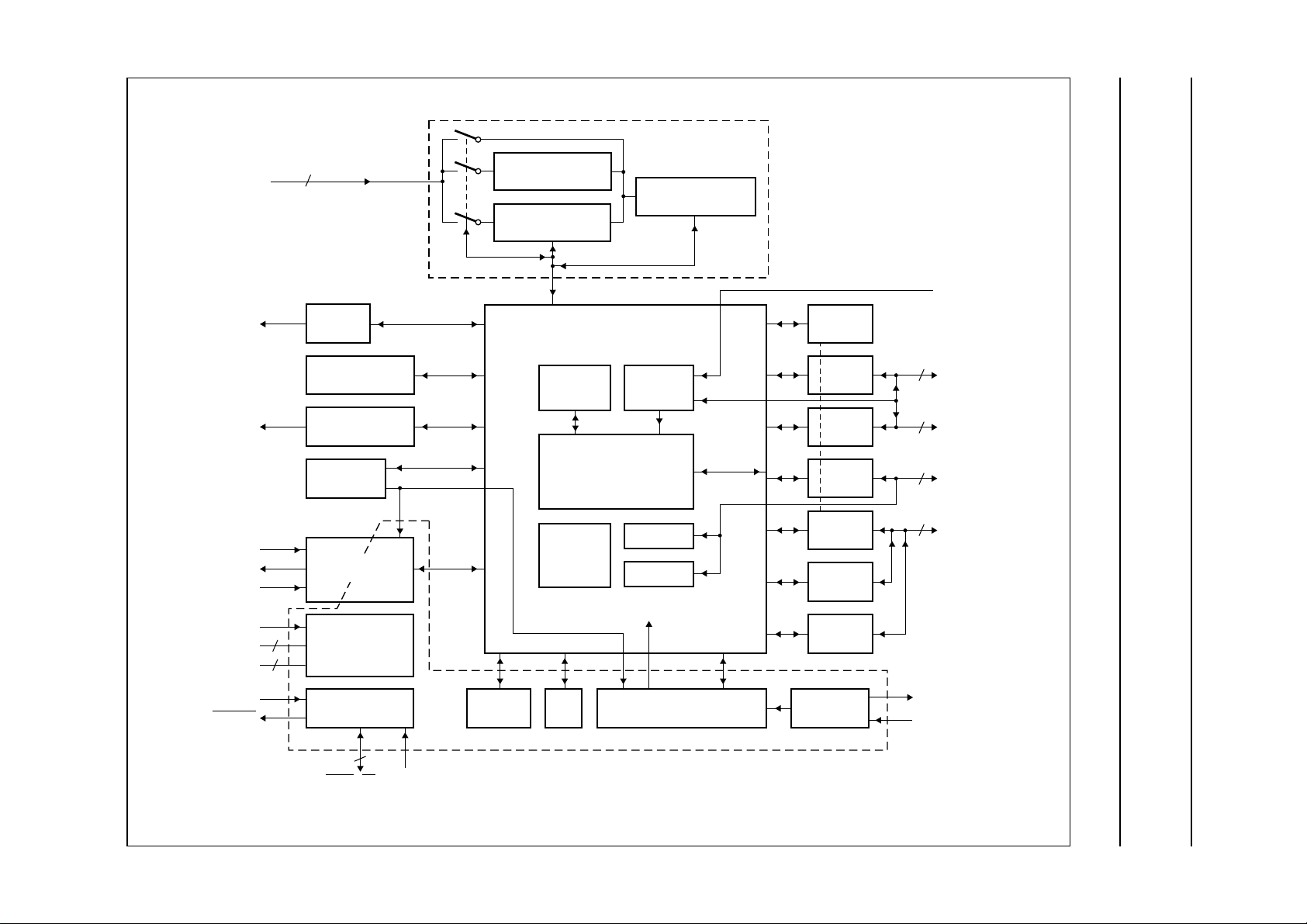
DIGITAL
FILTER
ZERO-IF
4L DEMODULATOR
I(D1), Q(D0)
AFCOUT
2
DAC
ndbook, full pagewidth
SYMBOL SAMPLING
CLOCK RECOVERY
PORT
CONTROL
V
PP
4 BLOCK DIAGRAM
Pager baseband controller PCA5010
Philips Semiconductors Product specification
AT
VIND
V
DD(DC)
V
SS(DC)
V
BAT
V
DD
V
SS
RESETIN
RESOUT
WATCHDOG
GENERATOR
6 MHz
OSCILLATOR
CONVERTER
2
2
CONTROLLER
MODE AND
TEST CONTROL
ALE, PSEN, EA TCLK
TONE
DC/DC
POWER
3
WAKE-UP
RAM
INTERRUPT
CONTROL
RTC
supplied by V
OTP/ROM
PROCESSOR
80C51
TIMER 0
TIMER 1
various clocks
CLOCK
GENERATOR
BAT
CLOCK
CORRECTION
P0
P2
P3
P1
UART SIO
I2C SIO
76.8 kHz
OSCILLATOR
MGR107
8
8
4
7
XTL2
XTL1
P0
P2
P3
(T0, T1,
INT0, INT1)
P1
(SDA, SCL,
RXD, TXD)
Fig.1 Block diagram.

Philips Semiconductors Product specification
Pager baseband controller PCA5010
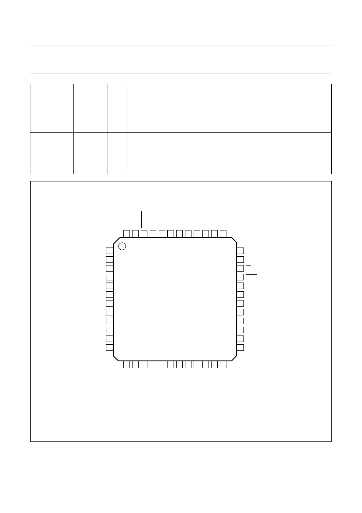
5 PINNING INFORMATION
SYMBOL PIN TYPE DESCRIPTION
P3.4 and P3.5 1 and 2 I/O Port 3: P3.4 and P3.5 are configured as push-pull outputs only (Option 3R, see
Section 6.6). Using the software input commands or the secondary port
function is possible by driving the Port 3 output lines accordingly:
P3.4 secondary function: T0 (counter input for T0)
P3.5 secondary function: T1 (counter input for T1)
AT 3 O Beeper high volume control output. Used to drive external bipolar transistor.
P2.0 to P2.7 4 to 11 I/O Port 2: Port 2 is an 8-bit bidirectional I/O port with internal pull-ups (option 1S,
see Section 6.6.3). As inputs, Port 2 pins that are externally pulled LOW will
source current because of the internal pull-ups. (See Chapter 10: I
emits the high-order address byte during fetches from external program
memory. In this application, it uses strong internal pull-ups when emitting
logic 1s. Port 2 is also used to control the parallel programming mode of the
on-chip OTP.
P0.0 to P0.4 12 to 16 I/O Port 0: Port 0 is a bidirectional I/O port with internal pull-ups (option 1S, see
Section 6.6.3). Port 0 pins that have logic 1s written to them are pulled HIGH by
the internal pull-ups and can be used as inputs. Port 0 is also the multiplexed
low-order address and data bus during access to external program and data
memory. In this application, it uses strong internal pull-ups when emitting
logic 1s. Port 0 also outputs the code bytes during OTP programming
verification.
V
DDA
17 S supply voltage for the analog parts of the PCA5010 and the
receiver/synthesizer control signals (Port 0 pins)
AFCOUT 18 O Buffered analog output of DAC for automatic receiver frequency control.
A voltage proportional to the offset of the receiver frequency can be generated.
Can be enabled/disabled by software.
I(D1) 19 I Input from receiver: may be demodulated NRZ signal or Zero-IF. In phase
limited signal.
Q(D0) 20 I Input from receiver: may be demodulated NRZ signal or Zero-IF. Quadrature
limited signal.
V
SSA
21 S ground signal reference (for the analog parts) (connected to substrate)
P0.5 to P0.7 22 to 24 I/O Port 0: Port 0 is a bidirectional I/O port with internal pull-ups (option 1R, 1R,
1S, see Section 6.6.3). Port 0 pins that have logic 1s written to them are pulled
HIGH by the internal pull-ups and can be used as inputs. Port 0 is also the
multiplexed low-order address and data bus during access to external program
and data memory. In this application, it uses strong internal pull-ups when
emitting logic 1s. Port 0 also outputs the code bytes during OTP programming
verification.
P1.0 to P1.2 25 to 27 I/O Port 1: Port 1 is an 8-bit quasi bidirectional I/O port with internal pull-ups.
Port 1 pins that have logic 1s written to them are pulled HIGH by the internal
pull-ups and can be used as inputs. As inputs, Port 1 pins that are externally
pulled LOW will source current because of the internal pull-ups. (See
Chapter 10: I
). P1.0 to P1.2 have external interrupts INT2 (X3) to INT4 (X5)
pu
assigned.
P1.3 28 I/O If the UART is disabled (ENS1 in S1CON.4 = 0) then P1.3 can be used as
general purpose P1 port pin. If the UART function is required, then a logic 1
must be written to P1.3. This I/O then becomes the RXD/data line of the UART.
). Port 2
pu
1998 Nov 02 6
Philips Semiconductors Product specification
Pager baseband controller PCA5010
SYMBOL PIN TYPE DESCRIPTION
P1.4 29 I/O If the UART is disabled (ENS1 in S1CON.4 = 0) then P1.4 can be used as
general purpose P1 port pin. If the UART function is required, then a logic 1
must be written to P1.4. This I/O then becomes the TXD/clock line of the UART.
P1.4 has external interrupt INT6 (X6) assigned.
V
SS
V
DD
ALE 32 I/O Address Latch Enable: Output pulse for latching the low byte of the address
PSEN 33 I/O Program Store Enable: The read strobe to external program memory. When
EA 34 I/O External Access Enable: EA must be externally held LOW to enable the
TCLK 35 I clock input for use as timing reference in external access mode and emulation
V
PP
P1.6 37 I/O If the I
P1.7 38 I/O If the I
XTL2 39 O output from the current source oscillator amplifier
XTL1 40 I input to the inverting oscillator amplifier and time reference for pager decoder,
V
BAT
V
DD(DC)
VIND 43 I Current input for the DC/DC converter. The booster inductor needs to be
V
SS(DC)
RESETIN 45 I Schmitt trigger reset input for the PCA5010. External R and C need to be
30 S ground (connected to substrate)
31 S supply voltage for the core logic and most peripheral drivers of the PCA5010
(see V
DDA
)
during an access to external memory.
the device is executing code from the external program memory, PSEN is
activated for each code byte fetch.
device to fetch code from external program memory locations 0000H to 7FFFH.
If EA is held HIGH, the device executes from internal program memory unless
the program counter contains an address greater the 7FFFH (32 kbytes).
36 S Programming voltage (12.5 V) for the OTP. Is connected to VSS in the
application.
2
C-bus is disabled (ENS1 in S1CON.6 = 0) then P1.6 can be used as
general purpose P1 port pin. If the I2C-bus function is required, then a logic 1
must be written to P1.6. This I/O then becomes the clock line of the I2C-bus.
P1.6 is equipped with an open-drain output buffer. The pin has no clamp diode
to VDD.
2
C-bus is disabled (ENS1 in S1CON.6 = 0) then P1.7 can be used as
general purpose P1 port pin. If the I2C-bus function is required, then a logic 1
must be written to P1.7. This I/O then becomes the data line of the I2C-bus.
P1.7 is equipped with an open-drain output buffer. The pin has no clamp diode
to VDD.
real-time clock and timers
41 S Supply terminal from battery . Is used for supplying parts of the chip that need to
operate at all times.
42 O Supply voltage output of the DC/DC converter. An external capacitor is
required.
connected externally.
44 S ground (connected to substrate) OTP
connected to the battery supply. All internal storage elements (except
microcontroller RAM) are initialized when this input is activated.
1998 Nov 02 7
Philips Semiconductors Product specification
Pager baseband controller PCA5010
SYMBOL PIN TYPE DESCRIPTION
RESOUT 46 O Monitor output for the emulation system. Is active (LOW) whenever a reset is
applied to the microcontroller (a reset can be forced by RESETIN, watchdog or
wake-up from DC/DC converter in off mode). A reset to the microcontroller
initializes all SFRs and port pins; it has no impact on the blocks operating from
V
.
BAT
P3.2 and P3.3 47 and 48 I/O Port 3: P3.2 and P3.3 are configured as push-pull output only (option 3R, see
Section 6.6). Using the software input commands or the secondary port
function is possible by driving the Port 3 output lines accordingly:
P3.2 secondary function: INT0 (external interrupt 0)
P3.3 secondary function:
handbook, full pagewidth
INT1 (external interrupt 1)
P3.4
P3.5
AT
P2.0
P2.1
P2.2
P2.3
P2.4
P2.5
P2.6
P2.7
P0.0
RESOUT
P3.3
P3.2
48
47
46
1
2
3
4
5
6
7
8
9
10
11
12
13
14
15
P0.1
P0.3
P0.2
SS(DC)
RESETIN
V
45
44
PCA5010H
16
17
P0.4
DDA
V
V
VIND
43
42
18
19
I(D1)
AFCOUT
V
41
20
Q(D0)
XTL1
40
21
SSA
V
XTL2
39
22
P0.5
P1.7
38
23
P0.6
P1.6
24 37
P0.7
36
35
34
33
32
31
30
29
28
27
26
25
V
PP
TCLK
EA
PSEN
ALE
V
DD
V
SS
P1.4
P1.3
P1.2
P1.1
P1.0
MGR336
BAT
DD(DC)
Fig.2 Pin configuration.
1998 Nov 02 8

Philips Semiconductors Product specification
Pager baseband controller PCA5010
6 FUNCTIONAL DESCRIPTION
6.1 General
The PCA5010 contains a high-performance CMOS
microcontroller and the required peripheral circuitry to
implement high-speed pagers for the modern paging
protocols. For this purpose, features such as FSK
demodulator, protocol timer, real-time clock and DC/DC
converter have been integrated on-chip.
The microcontroller embedded within the PCA5010
implements the standard 80C51 architecture and supports
the complete instruction set of the 80C51 with all
addressing modes.
The PCA5010 contains 32 kbytes of OTP program
memory; 1.25 kbyte of static read/write data memory,
27 I/O lines, two 16-bit timer/event counters, a
fifteen-source two priority-level, nested interrupt structure
and on-chip oscillator and timing circuit.
The PCA5010 devices have several software selectable
modes of reduced activity for power reduction; Idle for the
CPU and standby or off for the DC/DC converter. The Idle
mode freezes the CPU while allowing the RAM, timers,
serial I/O and interrupt system to continue functioning.
The standby mode for the DC/DC converter allows a high
efficiency of the latter at low currents and the off mode
reduces the supply voltage to the battery level. In the off
mode the RAM contents are preserved, real-time clock
and protocol timer are operating, but all other chip
functions are inoperative.
Two serial interfaces are provided on-chip; a UART serial
interface and an I
2
C-bus serial interface. The I2C-bus
serial interface has byte oriented master functions allowing
communication with a whole family of I2C-bus compatible
slave devices.
6.2 CPU timing
The internal CPU timing of the PCA5010 is completely
different to other implementations of this core. The CPU is
realized in asynchronous handshaking technology, which
results in extremely low power consumption and low EMC
noise generation.
6.2.1 B
ASICS
The implementation of the CPU of the PCA5010 as a block
in handshake technology has become possible through
the TANGRAM tool set, developed in the Philips Natlab in
Eindhoven.
TANGRAM is a high level programming language which
allows the description of parallel and sequential processes
that can be compiled into logic on silicon. The CPU has the
following features:
• No clock is needed. Every function within the CPU is self
timed and always runs at the maximum speed that a
given silicon die under the current operating conditions
(supply voltage and temperature) allows.
• The CPU fetches opcodes with maximum speed until a
special mode (e.g. Idle) is entered that stops this
sequence.
• Only bytes that are required are fetched from the
program memory. The dummy read cycles which exist in
the standard 80C51 have been omitted to save power.
• To further speed up the execution of a program, the next
sequential byte is always fetched from the code memory
during the execution of the current command. In the
event of jumps the prefetched byte is discarded.
• Since no clocks are required, the operating power
consumption is essentially lower compared to
conventional architectures and Idle power consumption
is reduced to nearly zero (leakage only).
• Clocks are only required as timing references for
timers/counters and for generating the timing to the
off-chip world.
6.2.2 E
XECUTION OF PROGRAMS FROM INTERNAL CODE
MEMORY
When code is executed in internal access mode (EA = 1),
the opcodes are fetched from the on-chip OTP. The OTP
is a self timed block which delivers data at maximum
speed. This is the preferred operating mode of the
PCA5010.
6.2.3 E
XECUTION OF PROGRAMS FROM EXTERNAL CODE
MEMORY
When code is executed in external access mode (EA = 0),
the opcodes are fetched from an off-chip memory using
the standard signals ALE, PSEN and P0, P2 for
multiplexed data and address information. In this mode the
identical hardware configurations as for a standard 80C51
system can be used, even if the timing for ALE and PSEN
is slightly different because it is generated from an internal
oscillator.
1998 Nov 02 9
Philips Semiconductors Product specification
Pager baseband controller PCA5010
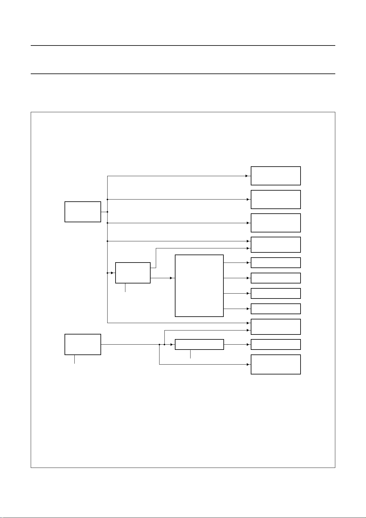
6.3 Overview on the different clocks used within the PCA5010
Figure 3 gives an overview on the clocks available within the PCA5010 for the different functions.
handbook, full pagewidth
76.8 kHz
OSCILLATOR
6 MHz
OSCILLATOR
OS6CON.7
CLOCK
CORRECTION
CCON.7
CORR
38.4 kHz
DIVIDER
FOR
THE
DIFFERENT
FREQUENCIES
DIVIDER
OS6CON.7
÷150
÷9600
÷2400
÷4
76.8 kHz
76.8 kHz
76.8 kHz
76.8 kHz
256 Hz
4 Hz
16 Hz
9.6 kHz
76.8 kHz
6 MHz
1.5 MHz
6 MHz
TONE GENERATOR
(both clock edges
are used)
UART
(both clock edges
are used)
TIMER 1
(both clock edges
are used)
DEMODULATOR/
CLOCK RECOVERY
TIMER 0
REAL-TIME CLOCK
WATCHDOG
WAKE-UP COUNTER
DC/DC CONVERTER
I2C-BUS
MICROCONTROLLER
OUTPUT AND
EXTERNAL ACCESS
MGL460
Fig.3 Overview on the clocks used within the PCA5010.
1998 Nov 02 10

Philips Semiconductors Product specification
Pager baseband controller PCA5010
6.4 Memory organization
The PCA5010 has a program memory (OTP) plus data
memory (RAM) on-chip. The device has separate address
spaces for Program and Data Memory (see Fig.4). If Ports
P0 and P2 are not used as I/O signals these pins can be
used to address up to 64 kbytes of external program
memory. In this case, the CPU generates the latch signal
(ALE) for an external address latch and the read strobe
(PSEN) for external Program Memory. External data
memory is not supported.
6.4.1 P
ROGRAM MEMORY
After reset the CPU begins execution of the program
memory at location 0000H. The program memory can be
implemented in either internal OTP or external memory.
If the EA pin is strapped to VDD, then program memory
fetches are directed to the internal program memory. If the
EA pin is strapped to VSS, then program memory fetches
are directed to external memory.
Programming the on-chip OTP is detailed in Chapter 15.
Usually Philips will deliver programmed parts to a
customer. Supply of blank engineering samples is
possible, but then Philips cannot give any guarantee on
the programmability and retention of the program memory.
6.4.2 D
ATA MEMORY
The PCA5010 contains 1280 bytes internal RAM
(consisting of 256 bytes standard RAM and 1024 bytes
AUX-RAM) and Special Function Registers (SFRs).
Figure 4 shows the internal data memory space divided
into the lower 128 bytes the upper 128 bytes and the SFR
space and 1024 bytes auxiliary RAM. Internal RAM
locations 0 to 127 are directly and indirectly addressable.
Internal RAM locations 128 to 255 are only indirectly
addressable. The SFR locations 128 to 255 bytes are only
directly addressable and the auxiliary RAM is indirectly
addressable as external RAM (MOVX). External Data
Memory (EDM) is not supported.
6.4.3 S
PECIAL FUNCTION REGISTERS
The second 128 bytes are the address locations of the
special function registers. Table 1 shows the special
function registers space. The SFRs include the port
latches, timers, peripheral control, serial I/O registers, etc.
These registers can only be accessed by direct
addressing. There are 128 bit addressable locations in the
SFR address space (those SFRs whose addresses are
divisible by eight).
handbook, full pagewidth
FFFFH
7FFFH
INTERNAL
(EAN = 1)
EXTERNAL
0
EXTERNAL
(EAN = 0)
FFH
INDIRECT
ADDRESSING
80H
7FH
INDIRECT AND
DIRECT
ADDRESSING
00H
Internal RAM
Fig.4 Memory map.
3FFH
INDIRECT
ADDRESSING
DIRECT
ADDRESSING
SFR space External XRAM
DATA MEMORYPROGRAM MEMORY
WITH DPTR
INDIRECT
ADDRESSING
WITH Ri, DPTR
Internal XRAM
100H
0FFH
000H
is not supported
MGL459
1998 Nov 02 11

Philips Semiconductors Product specification
Pager baseband controller PCA5010
6.5 Addressing
The PCA5010 has five methods for addressing source
operands:
• Register
• Direct
• Register-Indirect
• Immediate
• Base-Register plus Index-Register-Indirect.
The first three methods can be used for addressing
destination operands. Most instructions have a
‘destination/source’ field that specifies the data type,
addressing methods and operands involved.
For operations other than MOVs, the destination operand
is also a source operand.
Access to memory addressing is as follows:
• Registers in one of the four 8-register banks through
Register Direct or Register-Indirect
• Maximum 1280 bytes of internal data RAM through
Direct or Register-Indirect
– Bytes 0 to 127 of internal RAM may be addressed
directly/indirectly. Bytes 128 to 255 of internal RAM
share their address location with the SFRs and so
may only be addressed Register-Indirect as data
RAM.
– Bytes 0 to 1024 of AUX-RAM can be addressed
indirectly via MOVX. Bytes 256 to 1024 can only be
addressed using indirect addressing with the data
pointer, while bytes 0 to 255 may be also addressed
using R0 or R1.
• Special function registers through Direct
• Program memory Look-Up Tables (LUTs) through
Base-Register plus Index-Register-Indirect.
The PCA5010 is classified as an 8-bit device since the
internal ROM, RAM, Special Function Registers (SFRs),
Arithmetic Logic Unit (ALU) and external data bus are all
8-bits wide. It performs operations on bit, nibble, byte and
double-byte data types.
Facilities are available for byte transfer, logic and integer
arithmetic operations. Data transfer, logic and conditional
branch operations can be performed directly on Boolean
variables to provide excellent bit handling.
While the PCA5010 is executing code from the internal
memory, ALE and
ALE = LOW and PSEN = HIGH.
External XRAM is not supported for this device, since P3.7
(RD) and P3.6 (WR) pins are not available. If the external
XRAM is accessed accidentally, no PSEN or ALE cycle is
done and actual P0 values are read. Internal XRAM
access is not visible from outside the chip (no ALE, PSEN,
P0 and P2 activity).
PSEN pins are inactive with
1998 Nov 02 12

Philips Semiconductors Product specification
Pager baseband controller PCA5010
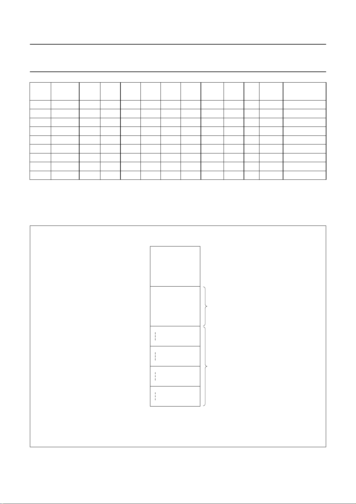
Table 1 Special Function Registers Overview; note 1
ADDR
(HEX)
NAME 7 6 5 4 3 2 1 0 R/W
RESET
VALUE
COMMENT
80 P0 RW 9FH bit addressable
81 SP RW 07H
82 DPL RW 00H
83 DPH RW 00H
87 PCON SMOD XRE ENIS − GF1 GF0 PD IDL RW 00H
88 TCON TF1 TR1 TF0 TR0 IE1 IT1 IE0 IT0 RW 00H bit addressable
89 TMOD GATE C/T M1 M0 GATE C/T M1 M0 RW 00H
8A TL0 RW 00H
8B TL1 RW 00H
8C TH0 RW 00H
8D TH1 RW 00H
90 P1 RW FFH bit addressable
92 TGCON ENB CLK2 −−−−−−RW 00H
93 TG0 RW 00H
94 WUCON RUN WUP TEST CPL Z1 Z0 LOAD SET RW 00H see note 2
95 WUC0 RW 00H see note 2
96 WUC1 RW 00H see note 2
98 S0CON SM0 SM1 − REN TB8 RB8 TI RI RW 00H bit addressable
99 S0BUF RW 00H
9E AFCON ENB − AFC5 AFC4 AFC3 AFC2 AFC1 AFC0 RW 00H
A0 P2 RW FFH bit addressable
A5 WDCON COND WD3 WD2 WD1 WD0 −−LD RW 00H
A8 IEN0/IE EA EWU ES1 ES0 ET1 EX1 ET0 EX0 RW 00H bit addressable
B0 P3 RW C3H bit addressable
B8 IP/IP0 − PWU PS1 PS0 PT1 PX1 PT0 PX0 RW 00H bit addressable
C0 IRQ1 IQ9 IQ8 IQ7 IQ6 IQ5 IQ4 IQ3 IQ2 RW 00H bit addressable
CD RTCON MIN −−−−W/
R LOAD SET RW 00H see note 2
CE RTC0 RW 00H see note 2
(3)
BLI
(3)
RW 00H bit addressable
(3)
RW 03H
D0 PSW CY AC F0 RS1 RS0 OV P
D1 DCCON0 OFF SBY RXE SBLI −−STB
D2 DCCON1 VBG1 VBG0 VLO1 VLO0 −−−−RW 00H
D3 OS6CON ENB −
SF4 SF3 SF2 SF1 SF0 MFR RW 00H
D4 OS6M0 R 00H
D8 S1CON − ENS1 STA STO SI AA − CR0 RW 00H bit addressable
D9 S1STA SC4 SC3 SC2 SC1 SC0 0 0 0 R 78H
DA S1DAT RW 00H
E0 ACC RW 00H bit addressable
E8 IEN1 EMIN EWD EDC EX6 ESC EX4 EX3 EX2 RW 00H bit addressable
E9 IX1 IL9 IL8 IL7 IL6 IL5 IL4 IL3 IL2 RW 00H
1998 Nov 02 13
Philips Semiconductors Product specification
Pager baseband controller PCA5010
ADDR
(HEX)
NAME 7 6 5 4 3 2 1 0 R/W
RESET
VALUE
COMMENT
EC DMD0 ENB M − RES LEV BD2 BD1 BD0 RW 00H
ED DMD1 ENA AVG6 AVG5 AVG4 AVG3 AVG2 AVG1 AVG0 R 00H ENA is RW
EE DMD2 ENC − BF − TEST B2 B1 B0 RW 00H
EF DMD3 RW 00H
F0 B RW 00H bit addressable
F8 IP1 PMIN PWD PDC PX6 PSC PX4 PX3 PX2 RW 00H bit addressable
FC CCON ENB PLUS TEST CIV17 CIV16 − BYPAS SET RW 00H
FD CC0 CIV7 CIV6 CIV5 CIV4 CIV3 CIV2 CIV1 CIV0 RW 00H
FE CC1 CIV15 CIV14 CIV13 CIV12 CIV11 CIV10 CIV9 CIV8 RW 00H
Notes
1. An empty field in this map indicates a bit that can be read or written to by software.
2. Value only reset with RESETIN and not or only partly with an off-restart sequence.
3. This bit cannot be changed by writing to it.
handbook, halfpage
7FH
30H
2FH
bit-addressable space
(bit addresses 0 to 7F)
20H
R7
R0
R7
R0
R7
R0
R7
R0
1FH
18H
17H
10H
0FH
08H
07H
4 banks of 8 registers
0
MLA560 - 1
(R0 to R7)
Fig.5 The lower 128 bytes of internal data memory.
1998 Nov 02 14

Philips Semiconductors Product specification
Pager baseband controller PCA5010
6.6 I/O facilities
6.6.1 P
The PCA5010 has 27 I/O lines treated as 27 individually
addressable bits or as four parallel 8-bit addressable ports.
Ports 0 and 2 are complete, Port 1 has only 7 and Port 3
has only 4 pins externally available. Ports 0, 1, 2 and 3
perform the following alternative functions:
Port 0 Is also used for external access, parallel OTP
Port 1 Used for a number of alternative functions (see
ORTS
programming mode and emulation (see Table 2 for
configuration details):
• Provides the multiplexed low-order address and
data bus for expanding the device with standard
memories and peripherals
• Provides access to the OTP data I/O lines in OTP
parallel programming mode.
Table 3 for configuration details):
• Provides the inputs for the external interrupts
INT2/P1.0 to INT4/P1.2 and INT6/P1.4
• SCL/P1.6 and SDA/P1.7 for the I2C-bus interface
are real open-drain outputs; no other port
configurations are available
• RXD/P1.3 and TXD/P1.4 for the UART data input
and output.
Port 3 Pins are configured as strong push-pull outputs
(see Table 5 for configuration details).
The following alternative Port 3 functions are
available, but to avoid short-circuiting of the
mentioned port pins, the input signals cannot be
applied externally to the Port 3 pins. The alternative
function can only be stimulated via the respective
port output function:
• External interrupt request inputs
INT1/P3.3
• Counter inputs T0/P3.4 and T1/P3.5.
To enable a port pin alternative function, the port bit latch
in its SFR must contain a logic 1.
Each port consists of a latch (SFRs P0 to P3), an output
driver and input buffer. Standard ports have internal
pull-ups. Figure 6a shows that the strong transistor p1 is
turned on for only a short time after a LOW-to-HIGH
transition in the port latch. When on, it turns on p3 (a weak
pull-up) through the inverter IN1. This inverter and p3 form
a latch which holds the logic 1.
6.6.2 P
I/O port output configurations are determined on-chip
according to one of the options shown in Fig.6. They
cannot be changed by software.
ORT I/O CONFIGURATION (OPTIONS)
INT0/P3.2 and
Port 2 Is also used for external access, parallel OTP
programming mode and emulation (see Table 4 for
configuration details):
• Provides the high-order address bus when
expanding the device with external program
memory
• Allows control of the on-chip OTP parallel
programming mode.
1998 Nov 02 15
Philips Semiconductors Product specification
Pager baseband controller PCA5010
handbook, full pagewidth
from port latch
input data
handbook, full pagewidth
V
weak pull-up
delay >50 ns
Q
strong pull-up
p1
n
V
SS
p2
hold pull-up
p3
IN1
V
DD
I/O pin
SS
MGR111
a. Standard/quasi-bidirectional (option 1).
V
from port latch
DD
strong pull-up
p1
Q
n
V
DD
I/O pin
handbook, full pagewidth
input data
from port latch
input data
c. Open-drain (only SDA/P1.7, SCL/P1.6) (option 2).
V
V
SS
SS
MGR112
b. Push-pull (option 3).
V
external
DD
I/O pin
Q
SLEW
RATE
CONTROL
V
SS
LOW-PASS
FILTER
n
V
SS
MGR113
external
pull-up
Fig.6 Port configuration options.
1998 Nov 02 16
Philips Semiconductors Product specification
Pager baseband controller PCA5010
6.6.3 PORT I/O CONFIGURATION
Tables 2 to 6 show the hardwired configuration for the different I/Os of the PCA5010.
Table 2 Port 0 configuration; notes 1 and 2
POSSIBLE
PORT PIN CONFIGURATION PULL-UP INPUT RESET DRIVE
P0.0 quasi bidirectional I/O (option 1S) yes hys HIGH 0.75 mA LCD_enable (O)
P0.1 quasi bidirectional I/O (option 1S) yes hys HIGH 0.75 mA SPI_enable (O)
P0.2 quasi bidirectional I/O (option 1S) yes hys HIGH 0.75 mA SPI_clock (O)
P0.3 quasi bidirectional I/O (option 1S) yes hys HIGH 0.75 mA SPI_data (O)
P0.4 quasi bidirectional I/O (option 1S) yes hys HIGH 0.75 mA SPI_data (I)
P0.5 quasi bidirectional I/O (option 1R) yes hys LOW 0.75 mA RXE (O)
P0.6 quasi bidirectional I/O (option 1R) yes hys LOW 0.75 mA ROE (O)
P0.7 quasi bidirectional I/O (option 1S) yes hys HIGH 0.75 mA bandwidth (O)/RSSI (I)
APPLICATION IN A
PAGER
Notes
1. Option 1S means port configuration option 1 with post-reset state set to HIGH; option 1R means post-reset state will
be LOW.
2. ‘hys’ means input stage with hysteresis.
Table 3 Port 1 configuration
POSSIBLE
PORT PIN CONFIGURATION PULL-UP INPUT RESET DRIVE
APPLICATION IN A
PAGER
P1.0 quasi bidirectional I/O (option 1S) yes hys HIGH 0.75 mA Key
P1.1 quasi bidirectional I/O (option 1S) yes hys HIGH 0.75 mA Key
P1.2 quasi bidirectional I/O (option 1S) yes hys HIGH 0.75 mA Key
P1.3 quasi bidirectional I/O (option 1S) yes hys HIGH 0.75 mA RXD
P1.4 quasi bidirectional I/O (option 1S) yes hys HIGH 0.75 mA TXD
P1.5 not available
P1.6 I
C-bus open-drain I/O (option 2S)
no hys HIGH 2.25 mA SCL
2
(slew rate limited)
P1.7 I
2
C-bus open-drain I/O (option 2S)
no hys HIGH 2.25 mA SDA
(slew rate limited)
Table 4 Port 2 configuration
POSSIBLE
PORT PIN CONFIGURATION PULL-UP INPUT RESET DRIVE
APPLICATION IN A
PAGER
P2.0 quasi bidirectional I/O (option 1S) yes hys HIGH 0.75 mA LCD_Data
P2.1 quasi bidirectional I/O (option 1S) yes hys HIGH 0.75 mA LCD_Data
P2.2 quasi bidirectional I/O (option 1S) yes hys HIGH 0.75 mA LCD_Data
P2.3 quasi bidirectional I/O (option 1S) yes hys HIGH 0.75 mA LCD_Data
1998 Nov 02 17
Philips Semiconductors Product specification
Pager baseband controller PCA5010
POSSIBLE
PORT PIN CONFIGURATION PULL-UP INPUT RESET DRIVE
P2.4 quasi bidirectional I/O (option 1S) yes hys HIGH 0.75 mA LCD_Data
P2.5 quasi bidirectional I/O (option 1S) yes hys HIGH 0.75 mA LCD_Data
P2.6 quasi bidirectional I/O (option 1S) yes hys HIGH 0.75 mA LCD_Data
P2.7 quasi bidirectional I/O (option 1S) yes hys HIGH 0.75 mA LCD_Data
Table 5 Port 3 configuration
PORT PIN CONFIGURATION PULL-UP INPUT RESET DRIVE
P3.0 not available
P3.1 not available
P3.2 push-pull output (option 3R) no hys LOW 3 mA call LED
P3.3 push-pull output (option 3R) no hys LOW 3 mA vibrator
P3.4 push-pull output (option 3R) no hys LOW 3 mA back light
P3.5 push-pull output (option 3R) no hys LOW 3 mA LCD R/
P3.6 not available
P3.7 not available
APPLICATION IN A
PAGER
POSSIBLE
APPLICATION IN A
PAGER
W/RXD enable
The port configuration is fixed and cannot be reconfigured by software or OTP code.
Table 6 Other pins
POSSIBLE
PORT PIN CONFIGURATION PULL-UP INPUT RESET DRIVE
AT push-pull output no LOW 3 mA tone generator output
I(D1) digital input no hys
Q(D0) digital input no hys
TCLK digital input no hys
RESETIN digital input no hys reset input
RESOUT push-pull output no LOW 1.5 mA reset output
XTL1 analog input/output (10 pF) no hys to crystal quartz
XTL2 analog input/output (10 pF) no to crystal quartz
AFCOUT analog output no
ALE quasi bidirectional I/O yes hys HIGH 1.5 mA
PSEN quasi bidirectional I/O yes hys HIGH 0.75 mA
EA 3-state I/O with bus keeper hold buffer HIGH 0.75 mA
APPLICATION IN A
PAGER
1998 Nov 02 18
Philips Semiconductors Product specification
Pager baseband controller PCA5010
6.7 Timer/event counters
The PCA5010 contains two 16-bit timer/event counters:
Timer 0 and Timer 1 which can perform the following
functions:
• Measure time intervals and pulse durations
• Count events
• Generate interrupt requests
• Generate output on comparator match
• Generate a Pulse Width Modulated (PWM) output
signal.
Timer 0 and Timer 1 can be programmed independently to
operate in four modes:
Mode 0 8-bit timer or 8-bit counter each with divide-by-32
prescaler.
Mode 1 16-bit time interval or event counter.
Mode 2 8-bit time interval or event counter with automatic
reload upon overflow.
Mode 3 this mode of the standard 80C51 is not available.
In the timer mode the timers count events on the XTL1
input. Timer 0 counts through a prescaler at a rate of
256 Hz and Timer 1 counts directly on both edges of the
XTL1 signal at a rate of 153.6 kHz. The nominal frequency
of the XTL1 signal is 76.8 kHz.
In the counter mode the register is incremented in
response to a HIGH-to-LOW transition at P3.4 (T0) and
P3.5 (T1).
Besides the different input frequencies and the
non-availability of Mode 3, both Timer 0 and Timer 1
behave exactly identical to the standard 80C51 Timer 0
and Timer 1.
handbook, full pagewidth
Detailed configuration of the 4 available modes is found in the 80C51 family hardware description (
XTL1
T0
Gate
INT0
XTL1
T1
Gate
INT1
÷ 300
256 Hz
C/T = 0
C/T = 1
TR0
153.6 kHz
C/T = 0
C/T = 1
TR1
Fig.7 Timer/counter 0 and 1: clock sources and control logic.
TL0
TL1 TH1
“Philips Semiconductors IC20 Data Handbook”
TH0
MGR114
).
1998 Nov 02 19

Philips Semiconductors Product specification
Pager baseband controller PCA5010
6.8 I2C-bus serial I/O
The serial port supports the 2-line I2C-bus which consists
of a data line (SDA) and a clock line (SCL). These lines
also function as the I/O port lines P1.7 and P1.6
respectively. The system is unique because data
transport, clock generation, address recognition and bus
control arbitration are all controlled by hardware. The
I2C-bus serial I/O has complete autonomy in byte
handling. The implementation in the PCA5010 operates in
single master mode as:
• Master transmitter
• Master receiver.
These functions are controlled by the S1CON register.
S1STA is the status register whose contents may also be
used as a vector to various service routines. S1DAT is the
data shift register. The block diagram of the I2C-bus
serial I/O is shown in Fig.8.
handbook, full pagewidth
SDA
ARBITRATION LOGIC
6.8.1 DIFFERENCES TO A STANDARD I2C-BUS INTERFACE
The I2C-bus interface of the PCA5010 implements the
standard for master receiver and transmitter as defined in
e.g. P83CL781/782 with the following restrictions:
• The baud rate is fixed to either 100 kHz (CR0 = 0) or
400 kHz (CR0 = 1) derived from the on-chip 6 MHz
oscillator. Therefore bits CR1 and CR2 in the S1CON
SFR are not available.
• Only single master functions are implemented.
– Slave address (S1ADR) is not available
– Status register (S1STA) reports only status defined
for the MST/TRX and MST/REC modes
– Multimaster operation is not supported.
SHIFT REGISTER
S1DAT
SCL BUS CLOCK GENERATOR
76543210
S1CON
76543210
S1STA
Fig.8 Block diagram of I2C-bus serial I/O.
INTERNAL BUS
MGL449
1998 Nov 02 20
Philips Semiconductors Product specification
Pager baseband controller PCA5010
2
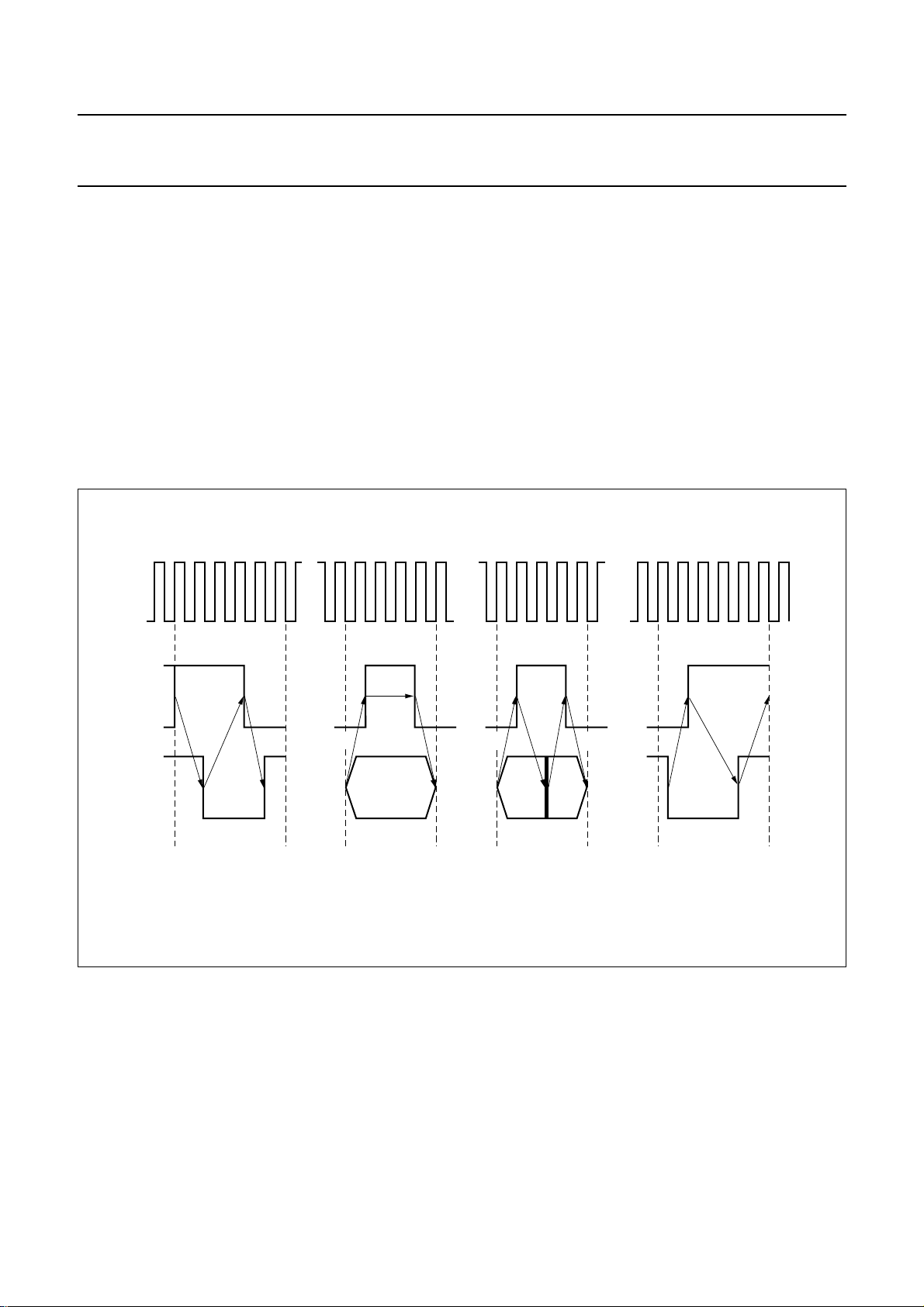
6.8.2 TIMING
The timing of the I2C-bus interface is based on the internal
6 MHz clock. The phases of this clock divided-by-4 are
used as a reference in the 400 kHz mode and
divided-by-16 in the 100 kHz mode. In the following
context ‘T’ (333 ns or 1.33 µs) denotes a single phase of
this clock.
The transfer of a single bit lasts 9 T. SCL is HIGH for 5 T.
When receiving data, the PCA5010 samples the SDA line
after 3 T while SCL is HIGH.
2
The implemented I
C-bus Interface operates according to
the timing diagram in Fig.9.
The open-drain I
rate controlled driver stages, to minimize the negative
impact of I2C-bus activity on the pager sensitivity while the
pager is receiving. Typical waveforms on P1.7 (SDA) and
P1.6 (SCL) are shown in Fig.10.
Because SDA and SCL are open-drain type I/Os, only the
falling edge is determined by the driver characteristics.
The static sink current when driving LOW and the slope of
the rising edges are determined by the capacitive I2C-bus
load and its resistive termination (pull-up to VDD).
C-bus outputs are implemented as slew
handbook, full pagewidth
SCL
SDA
3T
4T
START
2T
5T
2T
TX bit
2T
2T
2T
3T
RX bit
Fig.9 Timing of the I2C-bus interface.
2T 2T
5T
2T
STOP
MGR337
1998 Nov 02 21
Philips Semiconductors Product specification
Pager baseband controller PCA5010
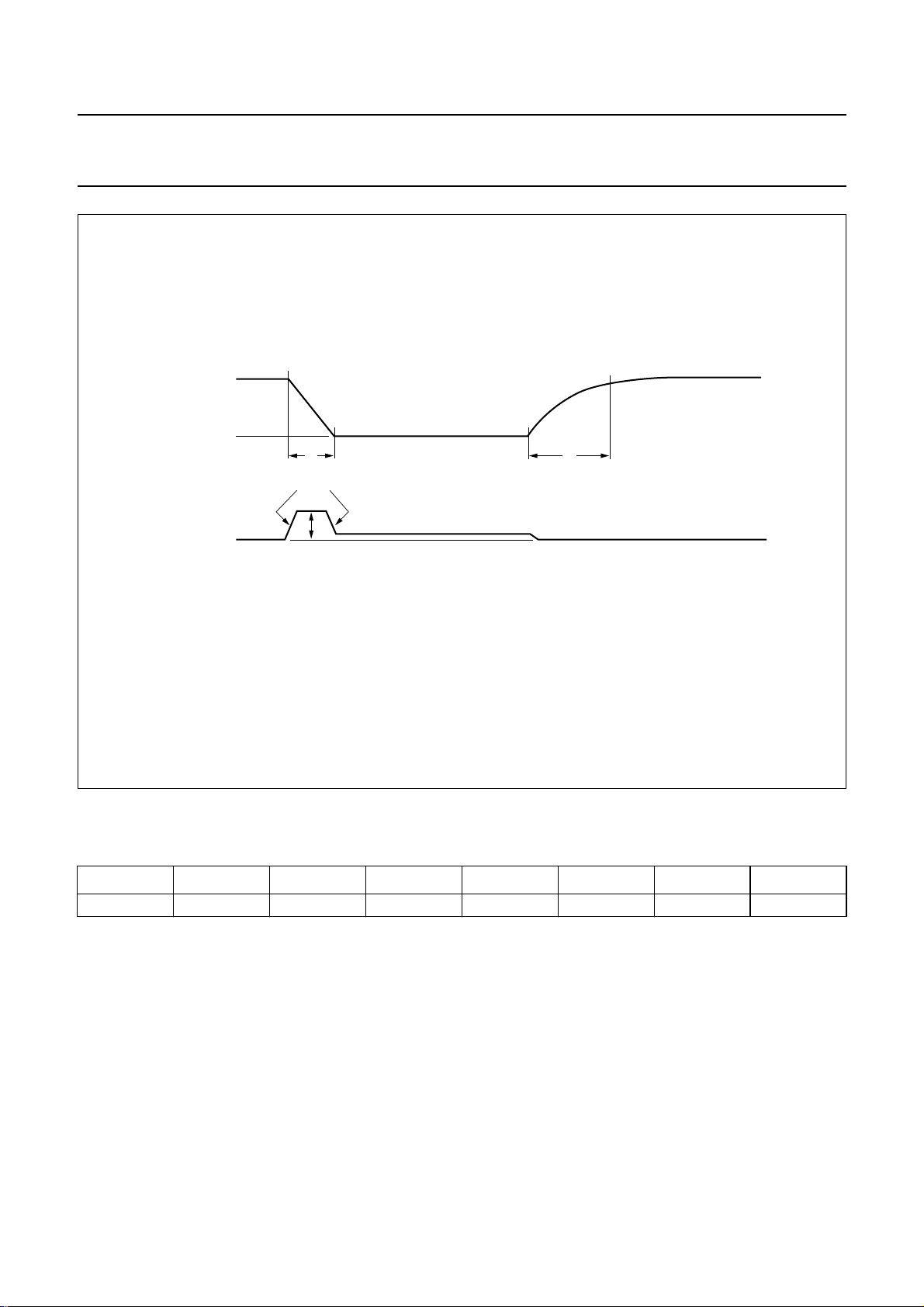
handbook, full pagewidth
voltage
(SDA, SCL)
sink current
(SDA, SCL)
(1) The falling slope depends on the capacitive load. Typical values at 2.2 V where CL= 50 pF are: tf= 100 ns; ISW= 2 mA; dl/dt = 250 µA/ns.
(2) The rising slope is defined by external pull-up resistor and capacitive load (a typical tr is 1 µs at 50 pF/20 kΩ.
V
DD
V
SS
t
dl/dt
I
SW
f
I
pu
(1)
t
r
(2)
MGR338
Fig.10 Typical waveforms on SDA and SCL.
6.8.3 SERIAL CONTROL REGISTER (S1CON)
Table 7 Serial Control Register (S1CON, SFR address D8H)
76543210
−ENS1 STA STO SI AA − CR0
1998 Nov 02 22

Philips Semiconductors Product specification
Pager baseband controller PCA5010
Table 8 Description of the S1CON bits
BIT SYMBOL FUNCTION
S1CON.7 − CR2 is not available.
S1CON.6 ENS1 Enable serial I/O. When ENS1 = 0, the serial I/O is disabled. SDA and SCL outputs are
in the high-impedance state; P1.6 and P1.7 function as open-drain ports. When
ENS1 = 1, the serial I/O is enabled. Output port latches P1.6 and P1.7 must be set to
logic 1.
S1CON.5 STA START flag. If ST A is set while the SIO is in master mode, SIO will generate a repeated
START condition.
S1CON.4 STO STOP flag. With this bit set while in master mode a STOP condition is generated. When
a STOP condition is detected on the I
S1CON.3 SI SIO interrupt flag. This flag is set, and an interrupt is generated, after any of the
following events occur:
• A START condition is generated in master mode
• A data byte has been received or transmitted in master mode (even if arbitration is
lost).
If this flag is set, the I
2
C-bus is halted (by pulling down SCL). Received data is only valid
until this flag is reset.
S1CON.2 AA Assert Acknowledge. When this bit is set, an acknowledge (LOW level to SDA) is
returned during the acknowledge clock pulse on the SCL line when:
• A data byte is received while the device is programmed to be a master receiver.
When this bit is reset, no acknowledge is returned.
S1CON.1 − CR1 is not available.
S1CON.0 CR0 Speed selection (with on-chip 6 MHz oscillator tuned to 6 MHz the nominal bus
frequency is:
CR0 = 0 is 83.3 kHz (6 MHz divided-by-72)
CR0 = 1 is 333 kHz (6 MHz divided-by-18).
2
C-bus, the SIO hardware clears the STO flag.
6.8.4 D
ATA SHIFT REGISTER (S1DAT)
S1DAT contains the serial data to be transmitted or data which has just been received. Bit 7 is transmitted or received
first; i.e. data shifted from left to right.
Table 9 Data Shift Register (S1DAT, SFR address DAH)
76543210
D7 D6 D5 D4 D3 D2 D1 D0
6.8.5 A
DDRESS REGISTER (S1ADR)
The slave address register is not available since slave mode is not supported.
1998 Nov 02 23
Philips Semiconductors Product specification
Pager baseband controller PCA5010
6.8.6 SERIAL STATUS REGISTER (S1STA)
The contents of this register may be used as a vector to a service routine. This optimizes the response time of the
software and consequently that of the I2C-bus. S1STA is a read-only register. The status codes for all available modes
of a single master I2C-bus interface are given in Tables 12 to 14.
Table 10 Serial Status Register (S1STA and SFR address D9H)
76543210
SC4 SC3 SC2 SC1 SC0 0 0 0
Table 11 Description of the S1STA bits
BIT SYMBOL FUNCTION
S1STA.3 to S1STA.7 SC4 to SC0 5-bit status code
S1STA.0 to S1STA.2 − these 3 bits are held LOW
Table 12 MST/TRX mode
S1STA VALUE DESCRIPTION
08H a START condition has been transmitted
10H a repeated START condition has been transmitted
18H SLA and W have been transmitted, ACK has been received
20H SLA and W have been transmitted,
28H DATA of S1DAT has been transmitted, ACK received
30H DATA of S1DAT has been transmitted,
Table 13 MST/REC mode
S1STA VALUE DESCRIPTION
40H SLA and R have been transmitted, ACK received
48H SLA and R have been transmitted,
50H DATA has been received, ACK returned
58H DATA has been received,
Table 14 Miscellaneous
S1STA VALUE DESCRIPTION
78H no information available (reset value); the serial interrupt flag SI, is not yet set
ACK returned
ACK received
ACK received
ACK received
1998 Nov 02 24

Philips Semiconductors Product specification
Pager baseband controller PCA5010
Table 15 Symbols used in Tables 12 to 14
SYMBOL DESCRIPTION
SLA 7-bit slave address
R read bit
W write bit
ACK acknowledgement (acknowledge bit = logic 0)
ACK no acknowledgement (acknowledge bit = logic 1)
2
DATA 8-bit data byte to or from I
MST master
SLV slave
TRX transmitter
REC receiver
C-bus
6.9 Serial interface SIO0: UART
The UART interface of the PCA5010 implements a subset
of the complete standard as defined in e.g. the P80CL580.
6.9.1 D
IFFERENCES TO THE STANDARD 80C51 UART
The following deviations from the standard exist:
• If [SM1 and SM0] = 10 then Mode 1 (8-bit data
transmission) is selected, with a fixed baud rate
(4800/9600 bits/s)
• If [SM1 and SM0] = 01 then Mode 2 (9-bit data
transmission) is selected, with a fixed baud rate
(4800/9600 bits/s)
• Modes 0 and 3 and the variable baud rate selection
using Timer 1 overflow is not available
• The SM2 bit has no function
• The time reference for modes 1 and 2 is taken from the
f
76.8 kHz oscillator, instead of the original
6.9.2 UART
MODES
OSC
----------12
This serial port is full duplex which means that it can
transmit and receive simultaneously. It is also
receive-buffered and can commence reception of a
second byte before a previously received byte has been
read from the register. However, if the first byte has not
been read by the time the reception of the second byte is
complete, the second byte will be lost. The serial port
receive and transmit registers are both accessed via the
special function register S0BUF. Writing to S0BUF loads
the transmit register and reading S0BUF accesses a
physically separate receive register.
The serial port can operate in 2 modes:
Mode 1 10 bits are transmitted (through TXD) or received
(through RXD): a START bit (0), 8 data bits (LSB
first) and a stop bit (1). On receive, the stop bit
goes into RB8 in special function register S0CON
(see Figs 11 and 12).
Mode 2 11 bits are transmitted (through TXD) or received
(through RXD): a start bit (0), 8 data bits (LSB
first), a programmable 9th data bit and a STOP
bit (1). On transmit, the 9th data bit (TB8 in
S0CON) can be assigned the value of 0 or 1.
Or, for example, the parity bit (P, in the PSW)
could be moved into TB8. On receive, the 9th
data bit goes into RB8 in S0CON, while the STOP
bit is ignored (see Figs 11 and 13).
In both modes the baud rate can be selected to either
4800 or 9600 depending on the SMOD bit in the PCON
SFR. If SMOD = 0 the baud rate is 4800, if SMOD = 1 the
baud rate is 9600 with a 76.8 kHz quartz.
In both modes, transmission is initiated by any instruction
that uses S0BUF as a destination register. Reception is
initiated by the incoming start bit if REN = 1.
6.9.3 S
ERIAL PORT CONTROL REGISTER (S0CON)
The serial port control and status register is the special
function register S0CON (see Table 16). The register
contains not only the mode selection bits, but also the 9th
data bit for transmit and receive (TB8 and RB8), and the
serial port interrupt bits (TI and RI).
1998 Nov 02 25
Philips Semiconductors Product specification
Pager baseband controller PCA5010
Table 16 Serial Port Control Register (S0CON, SFR address 98H)
76543210
SM0 SM1 − REN TB8 RB8 TI RI
Table 17 Description of the S0CON bits
BIT SYMBOL FUNCTION
S0CON.7 SM0 this bit along with the SM1 bit, is used to select the serial port mode; see Table 18
S0CON.6 SM1 this bit along with the SM0 bit, is used to select the serial port mode; see Table 18
S0CON.5 − SM2 is not available
S0CON.4 REN this bit enables serial reception and is set by software to enable reception, and cleared
by software to disable reception
S0CON.3 TB8 this bit is the 9th data bit that will be transmitted in Mode 2; set or cleared by software as
desired
S0CON.2 RB8 in Mode 2, this bit is the 9th data bit received; in Mode 1 it is the stop bit that was
received
S0CON.1 TI The transmit interrupt flag. Set by hardware at the end of the 8th bit time in Mode 0, or
at the beginning of the stop bit time in the other modes, in any serial transmission. Must
be cleared by software.
S0CON.0 RI The receive interrupt flag. Set by hardware at the end of the 8th bit time in Mode 0, or
halfway through the stop bit time in the other modes, in any serial transmission (for
exception see SM2). Must be cleared by software.
Table 18 Selection of the serial port modes
SM0 SM1 MODE DESCRIPTION BAUD RATE
1
⁄16f
0 1 1 8-bit UART
1 0 2 9-bit UART
6.9.4 UART
DATA REGISTER (S0BUF)
or1⁄8f
osc
1
⁄16f
osc
or1⁄8f
osc
osc
S0BUF contains the serial data to be transmitted or data which has just been received. Bit 0 is transmitted or received
first.
Table 19 Data Shift Register (S0BUF, SFR address 99H)
76543210
D7 D6 D5 D4 D3 D2 D1 D0
6.9.5 B
AUD RATES
The baud rate in Modes 1 and 2 depends on the value of the SMOD bit in SFR PCON and may be calculated as:
SMOD
Baud rate
2
---------------- -
• If SMOD = 0, (which is the value on reset), the baud rate is
• If SMOD = 1, the baud rate is1⁄8f
16
f
×=
osc
1
⁄16f
osc
.
osc
1998 Nov 02 26
Philips Semiconductors Product specification
Pager baseband controller PCA5010
handbook, full pagewidth
CSMOD at
PCON.7
XTL1
2
INTERNAL BUS
TB8
write to
SBUF
S
D
Q
CL
0
1
serial port
interrupt
sample
HIGH-TO-LOW
TRANSITION
DETECTOR
8
ZERO DETECTOR
STOP BIT SHIFT
START
TX CLOCK SEND
8
RX CLOCK R1
START
S0 BUFFER
TX CONTROL
T1
RX CONTROL
SHIFT
DATA
LOAD
SBUF
SHIFT
TXD
RXD
BIT
DETECTOR
INPUT SHIFT
LOAD
SBUF
READ
SBUF
INTERNAL BUS
REGISTER
(9-BITS)
S0 BUFFER
Fig.11 Serial port Mode 1 and Mode 2.
SHIFT
MGL452
1998 Nov 02 27
This text is here in white to force landscape pages to be rotated correctly when browsing through the pdf in the Acrobat reader.This text is here in
_white to force landscape pages to be rotated correctly when browsing through the pdf in the Acrobat reader.This text is here inThis text is here in
white to force landscape pages to be rotated correctly when browsing through the pdf in the Acrobat reader. white to force landscape pages to be ...
1998 Nov 02 28
TX CLOCK
WRITE TO SBUF
SEND
DATA
SHIFT
TXD
TI
RX CLOCK
R
RXD
E
C
E
BIT DETECTOR SAMPLE TIME
I
V
E
SHIFT
START BIT
D0
÷8 RESET
START BIT
D1
D2
D0 D1 D2 D3 D4 D5
D3
D4 D5
D6
D7
D6 D7
STOP BIT
STOP BIT
Philips Semiconductors Product specification
Pager baseband controller PCA5010
T
R
A
N
S
M
I
T
RI
MGL451
Fig.12 Serial port Mode 1 timing.
handbook, full pagewidth
This text is here in white to force landscape pages to be rotated correctly when browsing through the pdf in the Acrobat reader.This text is here in
_white to force landscape pages to be rotated correctly when browsing through the pdf in the Acrobat reader.This text is here inThis text is here in
white to force landscape pages to be rotated correctly when browsing through the pdf in the Acrobat reader. white to force landscape pages to be ...
1998 Nov 02 29
TX CLOCK
WRITE TO SBUF
SEND
DATA
SHIFT
TXD
TI
STOP BIT GEN
RX CLOCK
R
E
RXD
C
E
I
BIT DETECTOR SAMPLE TIME
V
E
SHIFT
RI
START BIT
D0 D1 D2
÷8 RESET
START BIT
D0 D1 D2 D3 D4 D5 D6 D7
D3 D4 D5 D6
D7 TB8
STOP BIT
RB8
STOP BIT
MGL450
Philips Semiconductors Product specification
Pager baseband controller PCA5010
T
R
A
N
S
M
I
T
handbook, full pagewidth
Fig.13 Serial port Mode 2 timing.
Philips Semiconductors Product specification
Pager baseband controller PCA5010
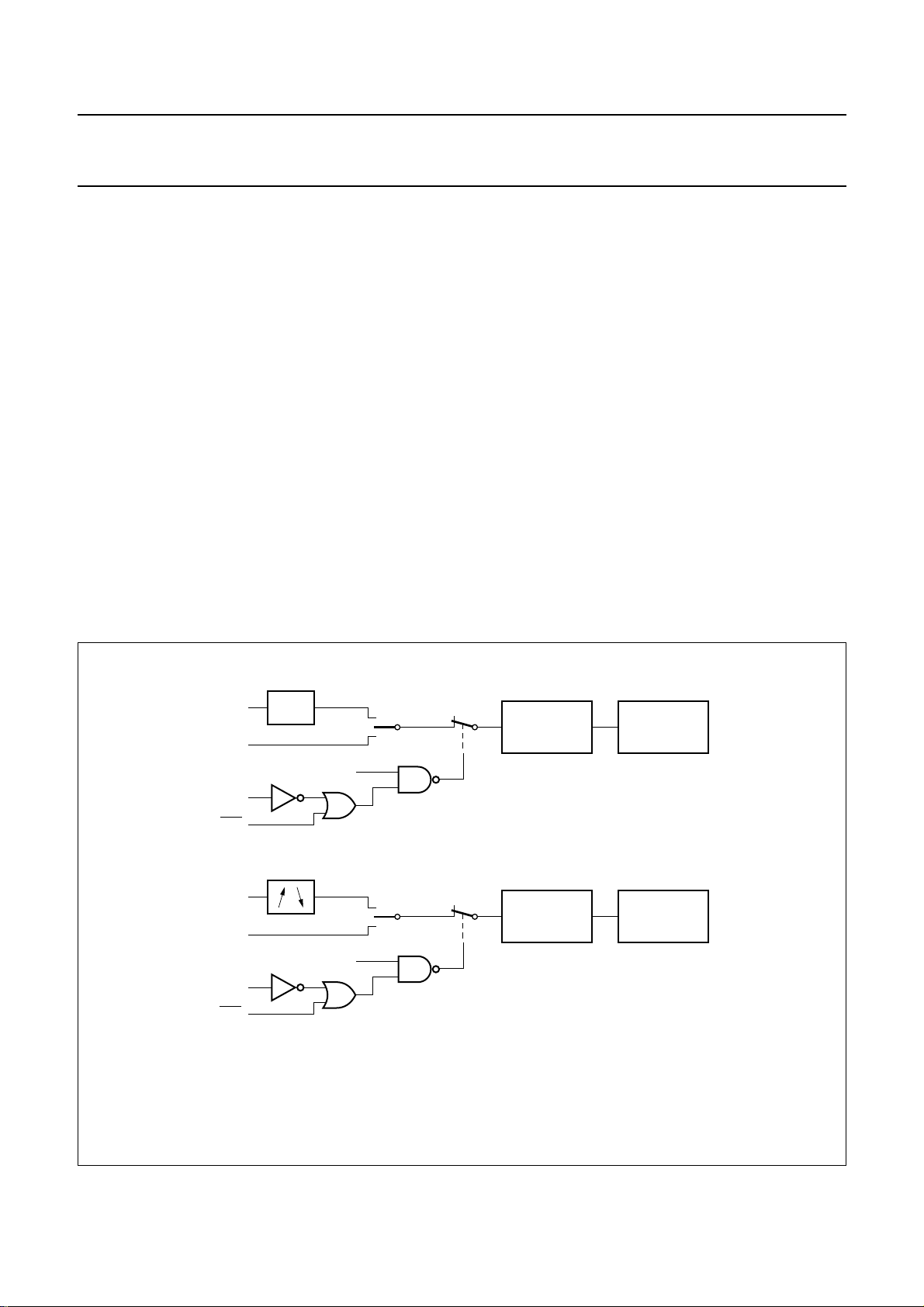
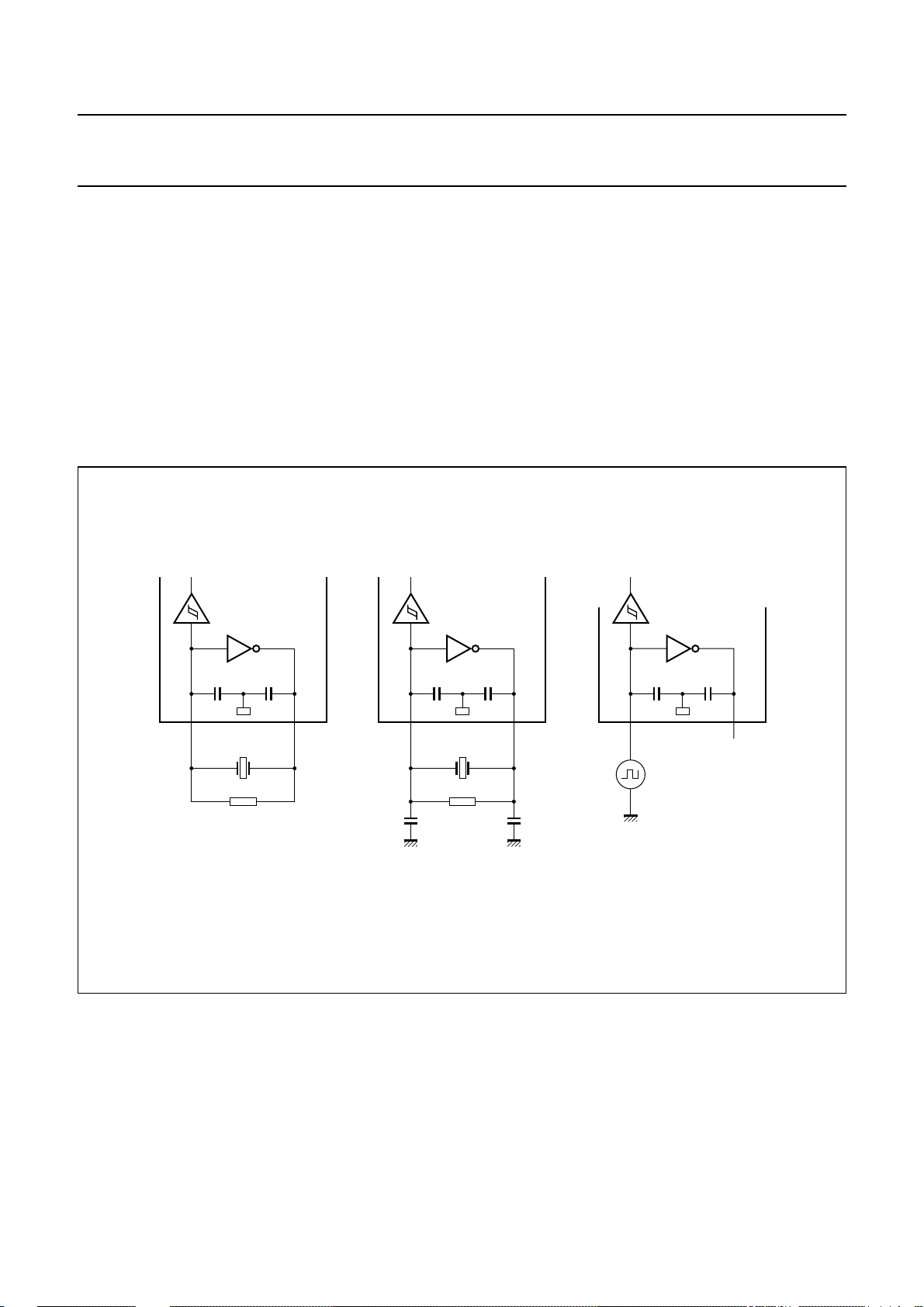
6.10 76.8 kHz oscillator
6.10.1 F
UNCTION
The oscillator produces a reference frequency of 76.8 kHz.
The frequency offset is compensated by a separate digital
clock correction block. The oscillator operates directly on
V
and is always enabled.
BAT
6.10.2 O
SCILLATOR CIRCUITRY
The on-chip inverting oscillator amplifier is a single NMOS
transistor supplied with a constant current. The amplitude
visible at terminals XTL1 and XTL2 is therefore not a full
handbook, full pagewidth
76.8 kHz 76.8 kHz 76.8 kHz
rail swing with a very high impedance. To reduce the
power consumption, the input Schmitt trigger buffer is
limited to approximately 100 kHz maximum frequency.
The whole circuit operates directly at the battery supply.
The 76.8 kHz oscillator cannot be disabled. It also
continues its operation during DC/DC converter off or
80C51 stop mode.
The simplest application configuration is shown in Fig.14a.
C1 and C2 can be added to operate a crystal at its optimal
load condition. The resulting capacitance of the series
connection of C1 and C2 must be smaller than 5 pF for a
guaranteed start-up of the oscillator.
10 pF
XTL1 XTL2
10 pF
XTL1 XTL2
76.8 kHz
2 MΩ
C1
(a) (b) (c)
10 pF10 pF
76.8 kHz
2 MΩ
C2
Fig.14 Oscillator circuit.
10 pF10 pF
XTL1 XTL2
VP = V
BAT
f
= 100 kHz
max
MGR115
1998 Nov 02 30
 Loading...