

Page 1

查询PCA5007供应商
INTEGRATED CIRCUITS
DATA SH EET
PCA5007
Pager baseband controller
Product specification
File under Integrated Circuits, IC17
1998 Oct 07
Page 2

Philips Semiconductors Product specification
Pager baseband controller PCA5007
CONTENTS
1 FEATURES
2 ORDERING INFORMATION
3 GENERAL DESCRIPTION
4 BLOCK DIAGRAM
5 PINNING
6 FUNCTIONAL DESCRIPTION
6.1 General
6.2 CPU timing
6.3 Overview on the different clocks used within
the PCA5007
6.4 Memory organization
6.5 Addressing
6.6 I/O facilities
6.7 Timer/event counters
6.8 I2C-bus serial I/O
6.9 Serial interface SIO0: UART
6.10 76.8 kHz oscillator
6.11 Clock correction
6.12 6 MHz oscillator
6.13 Real-time clock
6.14 Wake-up counter
6.15 Tone generator
6.16 Watchdog timer
6.17 2 or 4-FSK demodulator, filter and clock
recovery circuit
6.18 AFC-DAC
6.19 Interrupt system
6.20 Idle and power-down operation
6.21 Reset
6.22 DC/DC converter
7 INSTRUCTION SET
7.1 Instruction Map
8 LIMITING VALUES
9 EXTERNAL COMPONENTS
10 DC CHARACTERISTICS
11 AC CHARACTERISTICS
12 CHARACTERISTIC CURVES
13 TEST AND APPLICATION INFORMATION
14 APPENDIX 1: SPECIAL MODES OF THE
PCA5007
14.1 Overview
14.2 OTP parallel programming mode
14.3 Test modes
15 APPENDIX 2: THE PARALLEL
PROGRAMMING MODE
15.1 Introduction
15.2 General description
15.3 Entering the parallel programming mode
15.4 Address space
15.5 Single byte programming
15.6 Multiple byte programming
15.7 High voltage timing
15.8 OTP test modes
15.9 Signature bytes
15.10 Security
16 APPENDIX 3: OS SHEET
17 APPENDIX 4: BONDING PAD LOCATIONS
18 PACKAGE OUTLINE
19 SOLDERING
19.1 Introduction
19.2 Reflow soldering
19.3 Wave soldering
19.4 Repairing soldered joints
20 DEFINITIONS
21 LIFE SUPPORT APPLICATIONS
22 PURCHASE OF PHILIPS I2C COMPONENTS
1998 Oct 07 2
Page 3

Philips Semiconductors Product specification
Pager baseband controller PCA5007
1 FEATURES
• Operating temperature from: −10 to +55 °C
• Supply voltage range with on-chip DC/DC converter:
0.9 to 1.6 V
• Low operating and standby current consumption
• On-chip DC/DC converter generates the supply voltage
for the PCA5007 and external circuitry from a single cell
battery
• Battery low detector
• Low electromagnetic noise emission
• Full static asynchronous 80C51 CPU (8-bit CPU)
• Recovery from lowest power standby Idle mode to full
speed operation within microseconds
• 20 kbytes of One-Time Programmable (OTP) memory
and 1-kbyte of RAM on-chip
• 27 general purpose I/O port lines (4 ports with interrupt
possibility)
• 15 different interrupt sources with selectable priority
• 2 standard timer/event counters T0 and T1
2
C-bus serial port (single 100 kHz master transmitter
• I
and receiver)
• Subset of standard UART serial port (8 and 9-bit
transmission at 4800/9600 bits/s)
• 76.8 kHz crystal oscillator reference with digital clock
correction for real time and paging protocol
• Real-Time Clock (RTC)
• Receiver and synthesizer control
– Receiver control by software through general
purpose I/Os
– Synthesizer control by software through general
purpose I/Os
– 6-bit DAC for AFC to the receiver local oscillator
– Dedicated protocol timer.
• Decoding of paging data
– POCSAG or APOC phase 1, advanced high speed
paging protocols are also supported
– Supported data rates: 1200, 1600, 2400 and 3200
symbols/s using a 76.8 kHz crystal oscillator
– Demodulation of Zero-IF I andQ4or2level FSK
input or direct data input
– Noise filtering of data input and symbol clock
reconstruction
– De-interleaving, error checking and correction, sync
word detection address recognition, buffering and
more is done in software
– All user functions (keypad interface, alerter control,
display, etc.) are implemented in software.
• Musical tone generator for beeper, controlled by the
microcontroller
• Watchdog timer
• 48-pin LQFP package.
2 ORDERING INFORMATION
TYPE
NUMBER
(1)
PRODUCT TYPE
NAME DESCRIPTION VERSION
PCA5007H/XXX pre-programmed OTP LQFP48 plastic low profile quad flat package; 48 leads;
PACKAGE
SOT313-2
body 7 × 7 × 1.4 mm
Note
1. Please refer to the Order Entry Form (OEF) for this device for the full type number to use when ordering. This type
number will also specify the required OTP code.
1998 Oct 07 3
Page 4

Philips Semiconductors Product specification
Pager baseband controller PCA5007
3 GENERAL DESCRIPTION
The PCA5007 pager baseband controller is manufactured
in an advanced CMOS/OTP technology.
The PCA5007 is an 8-bit microcontroller especially suited
for pagers. For this purpose, features such as a
4 or 2 level FSK demodulator, filter, clock recovery,
protocol timer, DC/DC converter optimized for small
paging systems and RTC are integrated on-chip.
The device is optimized for low power consumption.
The PCA5007 has several software selectable modes for
power reduction: Idle and power-down mode of the
microcontroller, and standby and off mode of the DC/DC
converter.
The instruction set of the PCA5007 is based on that of the
80C51. The PCA5007 also functions as an arithmetic
processor having facilities for both binary and BCD
arithmetic plus bit-handling capabilities. The instruction set
consists of over 100 instructions: 49 one-byte,
46 two-byte, and 16 three-byte.
This data sheet details the properties of the PCA5007.
For details of the I
how to use it”
and features see
2
C-bus functions see
. For details on the basic 80C51 properties
“Data Handbook IC20”
“The I2C-bus and
.
1998 Oct 07 4
Page 5
Philips Semiconductors Product specification
Pager baseband controller PCA5007
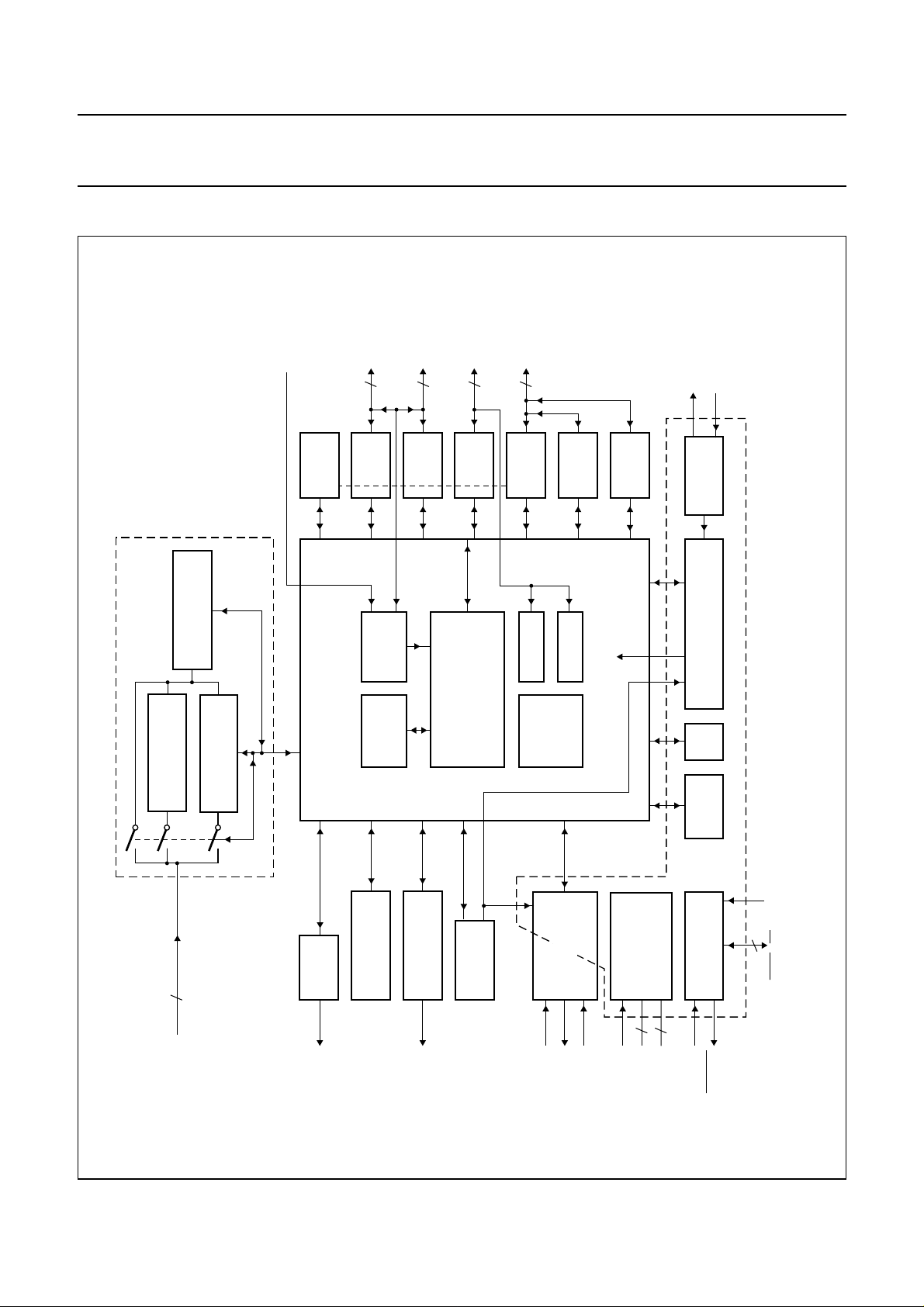
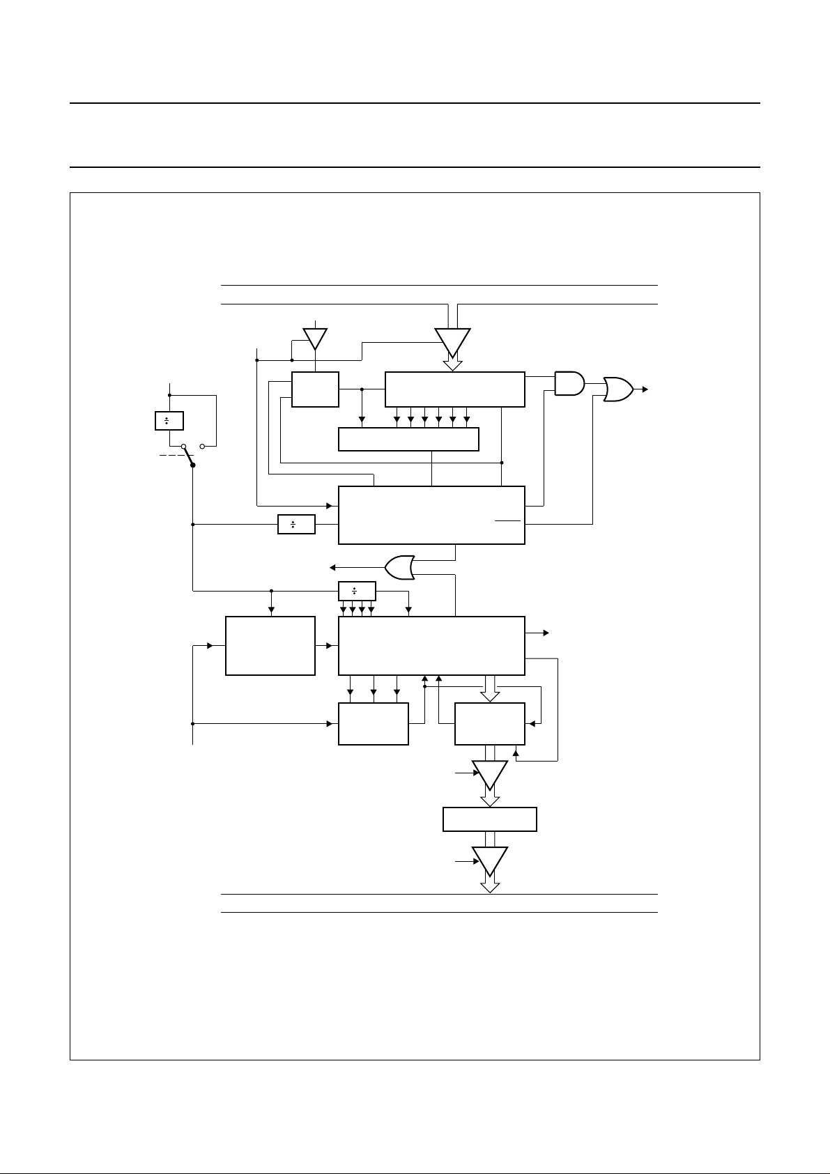
4 BLOCK DIAGRAM
ndbook, full pagewidth
CLOCK RECOVERY
SYMBOL SAMPLING
FILTER
DIGITAL
ZERO-IF
4L DEMODULATOR
V
PP
PORT
CONTROL
P0
8
P0
P2
8
P2
OTP/ROM
RAM
P3
(T0, T1,
INT0, INT1)P1(SDA, SCL,
4
P3
80C51
PROCESSOR
RXD, TXD)
7
P1
TIMER 0
INTERRUPT
UART SIO
TIMER 1
CONTROL
C SIO
2
I
various clocks
XTL2
XTL1
76.8 kHz
OSCILLATOR
CLOCK
CORRECTION
CLOCK
GENERATOR
BAT
RTC
supplied by V
MGR107
Fig.1 Block diagram.
This text is here in white to force landscape pages to be rotated correctly when browsing through the pdf in the Acrobat reader.This text is here in
_white to force landscape pages to be rotated correctly when browsing through the pdf in the Acrobat reader.This text is here inThis text is here in
white to force landscape pages to be rotated correctly when browsing through the pdf in the Acrobat reader. white to force landscape pages to be ...
1998 Oct 07 5
2
I(D1), Q(D0)
DAC
AFCOUT
TONE
WATCHDOG
AT
6 MHz
GENERATOR
OSCILLATOR
DC/DC
CONVERTER
VIND
DD(DC)
V
SS(DC)
V
POWER
CONTROLLER
2
2
DD
BAT
V
V
SS
V
WAKE-UP
MODE AND
TEST CONTROL
RESOUT
RESETIN
3
ALE, PSEN, EA TCLK
Page 6

Philips Semiconductors Product specification
Pager baseband controller PCA5007
5 PINNING
SYMBOL PIN TYPE DESCRIPTION
P3.4 and P3.5 1 and 2 I/O Port 3: P3.4 and P3.5 are configured as push-pull output only (option 3R; see
Section 6.6). Using the software input commands or the secondary port
function is possible by driving the port 3 output lines accordingly:
P3.4 secondary function: T0 (counter input for T0)
P3.5 secondary function: T1 (counter input for T1)
AT 3 O Beeper high volume control output. Used to drive external bipolar transistor.
P2.0 to P2.7 4 to 11 I/O Port 2: Port 2 is an 8-bit bidirectional I/O port with internal pull-ups (option 1S;
see Section 6.6.3). As inputs, port 2 pins that are externally pulled LOW will
source current because of the internal pull-ups. (see Chapter “DC
characteristics”: I
from external program memory. In this application, it uses strong internal
pull-ups when emitting logic 1s. Port 2 is also used to control the parallel
programming mode of the on-chip OTP.
P0.0 to P0.4 12 to 16 I/O Port 0: Port 0 is a bidirectional I/O port with internal pull-ups (option 1S; see
Section 6.6.3). Port 0 pins that have logic 1s written to them are pulled HIGH by
the internal pull-ups and can be used as inputs. Port 0 is also the multiplexed
low-order address and data bus during access to external program and data
memory. In this application, it uses strong internal pull-ups when emitting 1s.
Port 0 also outputs the code bytes during OTP programming verification.
V
DDA
17 S supply voltage for the analog parts of the PCA5007 and the
receiver/synthesizer control signals (Port 0 pins)
AFCOUT 18 O Buffered analog output of DAC for automatic receiver frequency control.
A voltage proportional to the offset of the receiver frequency can be generated.
Can be enabled/disabled by software.
I(D1) 19 I input from receiver: may be demodulated NRZ signal or Zero-IF. In phase
limited signal
Q(D0) 20 I input from receiver: may be demodulated NRZ signal or Zero-IF, Quadrature
limited signal.
V
SSA
21 S ground signal reference (for the analog parts) (connected to substrate)
P0.5 to P0.7 22 to 24 I/O Port 0: Port 0 is a bidirectional I/O port with internal pull-ups (option 1R,1R and
1S; see Section 6.6.3). Port 0 pins that have logic 1s written to them are pulled
HIGH by the internal pull-ups and can be used as inputs. Port 0 is also the
multiplexed low-order address and data bus during access to external program
and data memory. In this application, it uses strong internal pull-ups when
emitting 1s. Port 0 also outputs the code bytes during OTP programming
verification.
P1.0 to P1.2 25 to 27 I/O Port 1: Port 1 is an 8-bit quasi bidirectional I/O port with internal pull-ups.
Port 1 pins that have logic 1s written to them are pulled HIGH by the internal
pull-ups and can be used as inputs. As inputs, port 1 pins that are externally
pulled LOW will source current because of the internal pull-ups (see
Chapter “DC characteristics”: I
INT4 assigned.
P1.3 28 I/O If the UART is disabled (ENS1 in S1CON.4 = 0) then P1.3 can be used as
general purpose P1 port pin. If the UART function is required, then a logic 1
must be written to P1.3. This I/O then becomes the RXD/data line of the UART.
). Port 2 emits the high-order address byte during fetches
pu
). P1.0 to P1.2 have external interrupts INT2 to
pu
1998 Oct 07 6
Page 7
Philips Semiconductors Product specification
Pager baseband controller PCA5007
SYMBOL PIN TYPE DESCRIPTION
P1.4 29 I/O If the UART is disabled (ENS1 in S1CON.4 = 0) then P1.4 can be used as
general purpose P1 port pin. If the UART function is required, then a logic 1
must be written to P1.4. This I/O then becomes the TXD/clock line of the UART.
P1.4 has external interrupt INT6 (X6) assigned.
V
SS
V
DD
ALE 32 I/O Address Latch Enable: output pulse for latching the low byte of the address
PSEN 33 I/O Program Store Enable: the read strobe to external program memory. When
EA 34 I/O External Access Enable: EA must be externally held LOW to enable the
TCLK 35 I clock input for use as timing reference in external access mode and emulation
V
PP
P1.6(SCL) 37 I/O If the I
P1.7(SDA) 38 I/O If the I
XTL2 39 O output from the current source oscillator amplifier
XTL1 40 I input to the inverting oscillator amplifier and time reference for pager decoder,
V
BAT
V
DD(DC)
VIND 43 I Current input for the DC/DC converter. The booster inductor needs to be
V
SS(DC)
RESETIN 45 I Schmitt trigger reset input for the PCA5007. External R and C need to be
30 S ground (connected to substrate)
31 S supply voltage for the core logic and most peripheral drivers of the PCA5007
(see V
DDA
)
during an access to external memory.
the device is executing code from the external program memory, PSEN is
activated for each code byte fetch.
device to fetch code from external program memory locations 0000H to 4FFFH.
If EA is held HIGH, the device executes from internal program memory unless
the program counter contains an address greater the 4FFFH (20 kbytes).
36 S Programming voltage (12.5 V) for the OTP. Is connected to VSS in the
application.
2
C-bus is disabled (ENS1 in S1CON.6 = 0) then P1.6 can be used as
general purpose P1 port pin. If the I2C-bus function is required, then a logic 1
must be written to P1.6. This I/O then becomes the clock line of the I2C-bus.
P1.6 is equipped with an open-drain output buffer. The pin has no clamp diode
to VDD.
2
C-bus is disabled (ENS1 in S1CON.6 = 0) then P1.7 can be used as
general purpose P1 port pin. If the I2C-bus function is required, then a logic 1
must be written to P1.7. This I/O then becomes the data line of the I2C-bus.
P1.7 is equipped with an open-drain output buffer. The pin has no clamp diode
to VDD.
real-time clock and timers
41 S Supply terminal from battery . Is used for supplying parts of the chip that need to
operate at all times.
42 O Supply voltage output of the DC/DC converter. An external capacitor is
required.
connected externally.
44 S ground (connected to substrate) OTP
connected to the battery supply. All internal storage elements (except
microcontroller RAM) are initialized when this input is activated.
1998 Oct 07 7
Page 8
Philips Semiconductors Product specification
Pager baseband controller PCA5007
SYMBOL PIN TYPE DESCRIPTION
RESOUT 46 O Monitor output for the emulation system. Is active (LOW) whenever a reset is
applied to the microcontroller. (a reset can be forced by RESETIN, watchdog or
wake-up from DC/DC converter in off mode). A reset to the microcontroller
initializes all SFRs and port pins; it has no impact on the blocks operating from
V
.
BAT
P3.2 to P3.3 47 and 48 I/O Port 3: P3.2 and P3.3 are configured as push-pull output only (option 3R; see
Section 6.6). Using the software input commands or the secondary port
function is possible by driving the port 3 output lines accordingly:
P3.2 secondary function: INT0 (external interrupt 0)
P3.3 secondary function: INT1 (external interrupt 1)
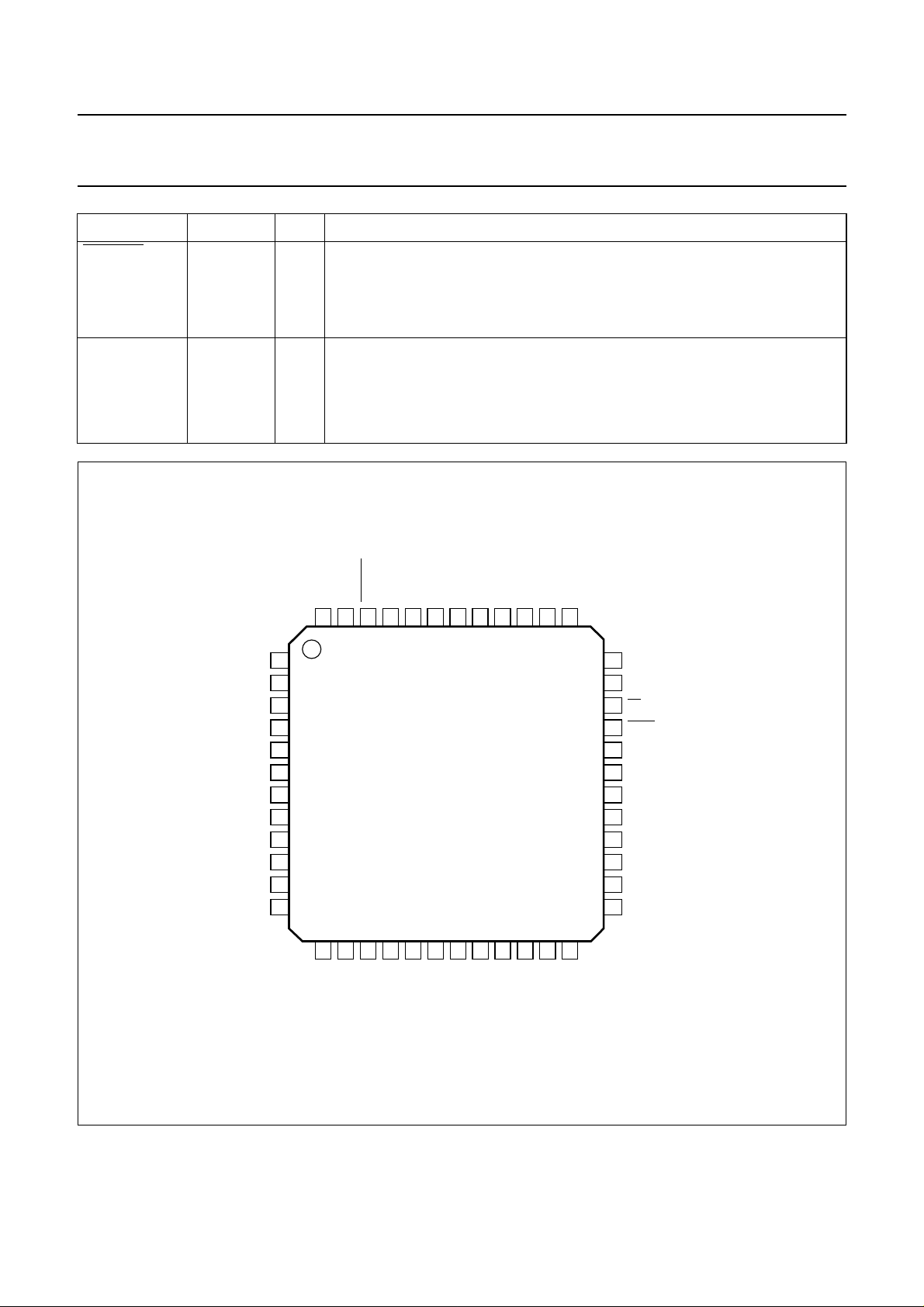
handbook, full pagewidth
P3.4
P3.5
AT
P2.0
P2.1
P2.2
P2.3
P2.4
P2.5
P2.6
P2.7
P0.0
BAT
DD(DC)
P0.3
SS(DC)
RESETIN
V
45
44
PCA5007H
16
17
P0.4
DDA
V
V
VIND
43
42
18
19
I(D1)
AFCOUT
V
41
20
Q(D0)
XTL1
40
21
SSA
V
XTL2
39
22
P0.5
P1.7
38
23
P0.6
P1.6
24 37
P0.7
36
35
34
33
32
31
30
29
28
27
26
25
V
PP
TCLK
EA
PSEN
ALE
V
DD
V
SS
P1.4
P1.3
P1.2
P1.1
P1.0
MGR108
RESOUT
P3.3
P3.2
48
47
46
1
2
3
4
5
6
7
8
9
10
11
12
13
14
15
P0.1
P0.2
Fig.2 Pin configuration.
1998 Oct 07 8
Page 9

Philips Semiconductors Product specification
Pager baseband controller PCA5007
6 FUNCTIONAL DESCRIPTION
6.1 General
The PCA5007 contains a high-performance CMOS
microcontroller and the required peripheral circuitry to
implement high-speed pagers for the modern paging
protocols. For this purpose, features such as FSK
demodulator, protocol timer, real-time clock and DC/DC
converter have been integrated on-chip.
The microcontroller embedded within the PCA5007
implements the standard 80C51 architecture and supports
the complete instruction set of the 80C51 with all
addressing modes.
The PCA5007 contains 20 kbytes of OTP program
memory; 1-kbyte of static read/write data memory,
27 I/O lines, two 16-bit timer/event counters, a
fifteen-source two priority-level, nested interrupt structure
and on-chip oscillator and timing circuit.
The PCA5007 devices have several software selectable
modes of reduced activity for power reduction; Idle for the
CPU and standby or off for the DC/DC converter. The Idle
mode freezes the CPU while allowing the RAM, timers,
serial I/O and interrupt system to continue functioning.
The standby mode for the DC/DC converter allows a high
efficiency of the latter at low currents and the off mode
reduces the supply voltage to the battery level. In the off
mode the RAM contents are preserved, the real-time clock
and protocol timer are operating, but all other chip
functions are inoperative.
Two serial interfaces are provided on-chip; a UART serial
interface and an I
2
C-bus serial interface. The I2C-bus
serial interface has byte oriented master functions allowing
communication with a whole family of I2C-bus compatible
slave devices.
6.2 CPU timing
The internal CPU timing of the PCA5007 is completely
different to other implementations of this core. The CPU is
realized in asynchronous handshaking technology, which
results in extremely low power consumption and low EMC
noise generation.
6.2.1 B
ASICS
The implementation of the CPU of the PCA5007 as a block
in handshake technology has become possible through
the TANGRAM tool set, developed in the Philips Natlab in
Eindhoven.
TANGRAM is a high level programming language which
allows the description of parallel and sequential processes
that can be compiled into logic on silicon. The CPU has the
following features:
• No clock is needed. Every function within the CPU is self
timed and always runs at the maximum speed that a
given silicon die under the current operating conditions
(supply voltage and temperature) allows.
• The CPU fetches opcodes with maximum speed until a
special mode (e.g. Idle) is entered that stops this
sequence.
• Only bytes that are required are fetched from the
program memory. The dummy read cycles which exist in
the standard 80C51 have been omitted to save power.
• To further speed up the execution of a program, the next
sequential byte is always fetched from the code memory
during the execution of the current command. In the
event of jumps the prefetched byte is discarded.
• Since no clocks are required, the operating power
consumption is essentially lower compared to
conventional architectures and Idle power consumption
is reduced to nearly zero (leakage only).
• Clocks are only required as timing references for
timers/counters and for generating the timing to the
off-chip world.
6.2.2 E
XECUTION OF PROGRAMS FROM INTERNAL CODE
MEMORY
When code is executed in internal access mode (EA = 1),
the opcodes are fetched from the on-chip OTP. The OTP
is a self timed block which delivers data at maximum
speed. This is the preferred operating mode of the
PCA5007.
6.2.3 E
XECUTION OF PROGRAMS FROM EXTERNAL CODE
MEMORY
When code is executed in external access mode (EA = 0),
the opcodes are fetched from an off-chip memory using
the standard signals ALE, PSEN and P0, P2 for
multiplexed data and address information. In this mode the
identical hardware configurations as for a standard 80C51
system can be used, even if the timing for ALE and PSEN
is slightly different because it is generated from an internal
oscillator.
1998 Oct 07 9
Page 10
Philips Semiconductors Product specification
Pager baseband controller PCA5007
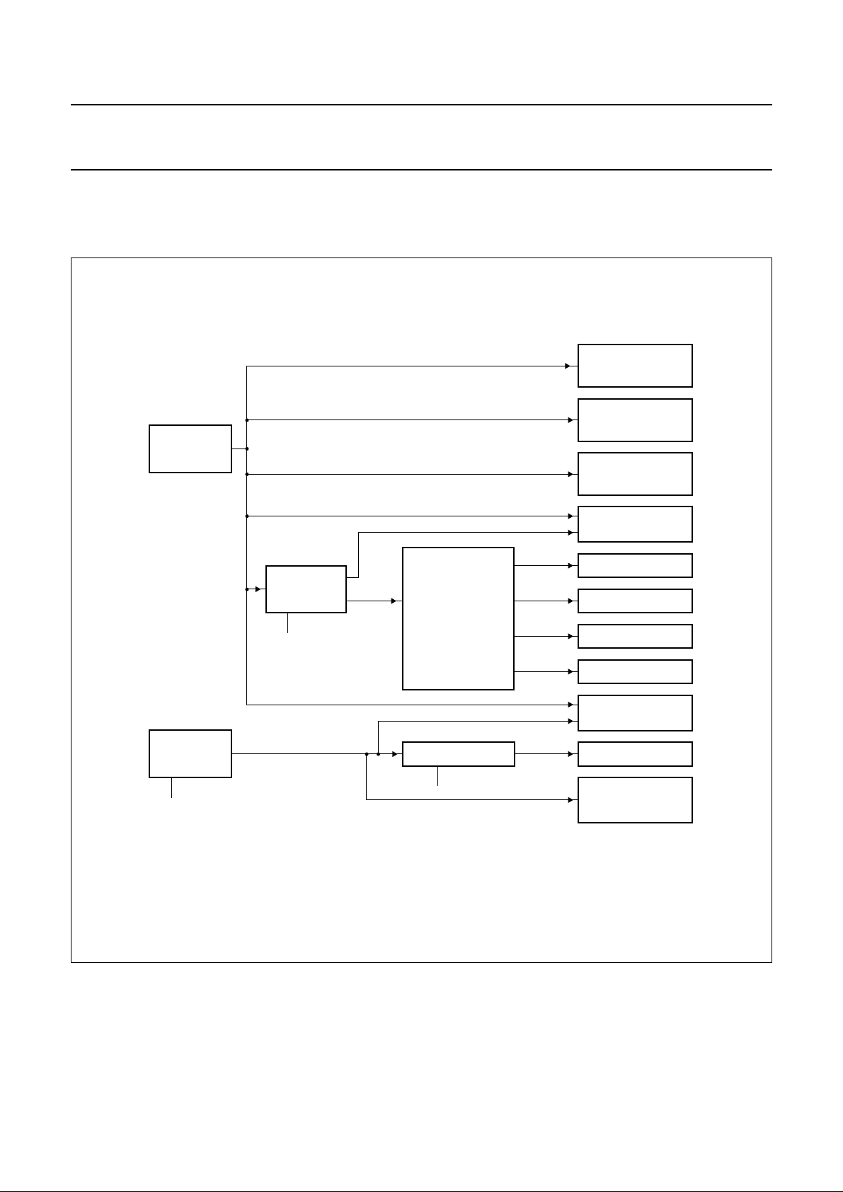
6.3 Overview on the different clocks used within the PCA5007
Figure 3 gives an overview on the clocks available within the PCA5007 for the different functions.
handbook, full pagewidth
76.8 kHz
OSCILLATOR
6 MHz
OSCILLATOR
OS6CON.7
CLOCK
CORRECTION
CCON.7
CORR
38.4 kHz
DIVIDER
FOR
THE
DIFFERENT
FREQUENCIES
DIVIDER
OS6CON.7
÷150
÷9600
÷2400
÷4
76.8 kHz
76.8 kHz
76.8 kHz
76.8 kHz
256 Hz
4 Hz
16 Hz
9.6 kHz
76.8 kHz
6 MHz
400 kHz
6 MHz
TONE GENERATOR
(both clock edges
are used)
UART
(both clock edges
are used)
TIMER 1
(both clock edges
are used)
DEMODULATOR/
CLOCK RECOVERY
TIMER 0
REAL-TIME CLOCK
WATCHDOG
WAKE-UP COUNTER
DC/DC CONVERTER
I2C-BUS
MICROCONTROLLER
OUTPUT AND
EXTERNAL ACCESS
MGR109
Fig.3 Overview on the clocks used within the PCA5007.
1998 Oct 07 10
Page 11

Philips Semiconductors Product specification
Pager baseband controller PCA5007
6.4 Memory organization
The PCA5007 has a program memory (OTP) plus data
memory (RAM) on-chip. The device has separate address
spaces for program and data memory (see Fig.4). If ports
P0 and P2 are not used as I/O signals these pins can be
used to address up to 64 kbytes of external program
memory. In this case, the CPU generates the latch signal
(ALE) for an external address latch and the read strobe
(PSEN) for external program memory. External data
memory is not supported.
6.4.1 P
ROGRAM MEMORY
After reset the CPU begins execution of the program
memory at location 0000H. The program memory can be
implemented in either internal OTP or external memory.
If the EA pin is strapped to VDD, then program memory
fetches are directed to the internal program memory. If the
EA pin is strapped to VSS, then program memory fetches
are directed to external memory.
Programming the on-chip OTP is detailed in Chapter 15.
Usually Philips will deliver programmed parts to a
customer. Supply of blank engineering samples is
possible, but then Philips cannot give any guarantee on
the programmability and retention of the program memory.
6.4.2 D
ATA MEMORY
The PCA5007 contains 1024 bytes of internal RAM
(consisting of 256 bytes standard RAM and 768 bytes
AUX-RAM) and Special Function Registers (SFRs).
Figure 4 shows the internal data memory space divided
into the lower 128 bytes the upper 128 bytes and the SFR
space and 768 bytes auxiliary RAM. Internal RAM
locations 0 to 127 are directly and indirectly addressable.
Internal RAM locations 128 to 255 are only indirectly
addressable. The SFR locations 128 to 255 are only
directly addressable and the auxiliary RAM is indirectly
addressable as external RAM (MOVX). External Data
Memory (EDM) is not supported.
6.4.3 S
PECIAL FUNCTION REGISTERS
The second 128 bytes are the address locations of the
special function registers. Table 1 shows the special
function registers space. The SFRs include the port
latches, timers, peripheral control, serial I/O registers, etc.
These registers can only be accessed by direct
addressing. There are 128 bit addressable locations in the
SFR address space (those SFRs whose addresses are
divisible by eight).
handbook, full pagewidth
FFFFH
4FFFH
INTERNAL
(EAN = 1)
EXTERNAL
0
EXTERNAL
(EAN = 0)
FFH
INDIRECT
ADDRESSING
80H
7FH
INDIRECT AND
DIRECT
ADDRESSING
00H
Internal RAM
Fig.4 Memory map.
2FFH
INDIRECT
ADDRESSING
DIRECT
ADDRESSING
SFR space External XRAM
DATA MEMORYPROGRAM MEMORY
WITH DPTR
INDIRECT
ADDRESSING
WITH Ri, DPTR
Internal XRAM
100H
0FFH
000H
is not supported
MGR110
1998 Oct 07 11
Page 12

Philips Semiconductors Product specification
Pager baseband controller PCA5007
6.5 Addressing
The PCA5007 has five methods for addressing source
operands:
• Register
• Direct
• Register-Indirect
• Immediate
• Base-Register plus Index-Register-Indirect.
The first three methods can be used for addressing
destination operands. Most instructions have a
‘destination/source’ field that specifies the data type,
addressing methods and operands involved. For
operations other than MOVs, the destination operand is
also a source operand.
Access to memory addressing is as follows:
• Registers in one of the four 8-register banks through
Register-Direct or Register-Indirect
• Maximum 1024 bytes of internal data RAM through
Direct or Register-Indirect
– Bytes 0 to 127 of internal RAM may be addressed
directly/indirectly. Bytes 128 to 255 of internal RAM
share their address location with the SFRs and so
may only be addressed Register-Indirect as data
RAM.
– Bytes 0 to 768 of AUX-RAM can only be addressed
indirectly via MOVX. Bytes 256 to 768 can only be
addressed using indirect addressing with the data
pointer, while bytes 0 to 255 may be also addressed
using R0 or R1.
• Special function registers through Direct
• Program memory Look-Up Tables (LUTs) through
Base-Register plus Index-Register-Indirect.
The PCA5007 is classified as an 8-bit device since the
internal ROM, RAM, Special Function Registers (SFRs),
Arithmetic Logic Unit (ALU) and external data bus are all
8 bits wide. It performs operations on bit, nibble, byte and
double-byte data types.
Facilities are available for byte transfer, logic and integer
arithmetic operations. Data transfer, logic and conditional
branch operations can be performed directly on Boolean
variables to provide excellent bit handling.
While the PCA5007 is executing code from the internal
memory, ALE and
ALE = LOW and PSEN = HIGH.
External XRAM is not supported for this device, since
P3.7 (RD) and P3.6 (WR) pins are not available. If the
external XRAM is accessed accidentally, no PSEN or ALE
cycle is done and actual P0 values are read. Internal
XRAM access is not visible from outside the chip (no ALE,
PSEN, P0 and P2 activity).
PSEN pins are inactive with
1998 Oct 07 12
Page 13

Philips Semiconductors Product specification
Pager baseband controller PCA5007
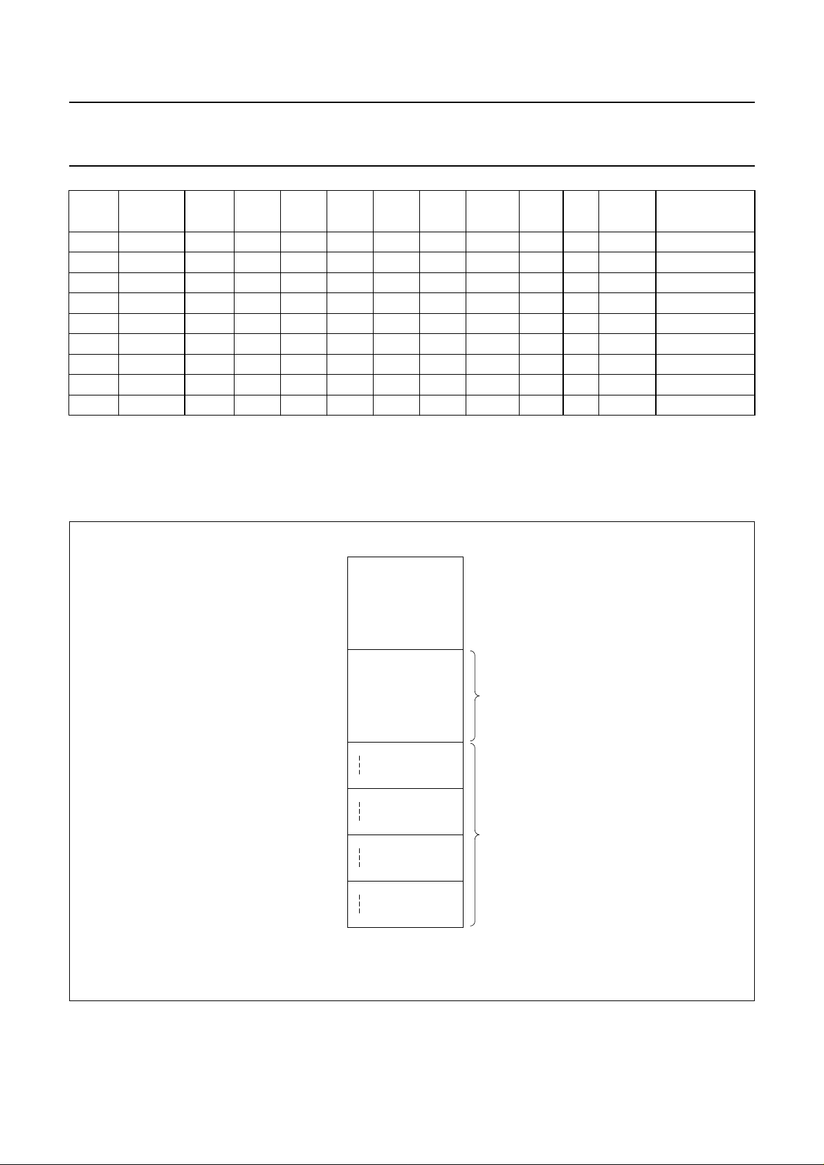
Table 1 Special Function Registers Overview; note 1
ADDR
(HEX)
NAME 7 6 5 4 3 2 1 0 R/W
RESET
VALUE
COMMENT
80 P0 R/W 9FH bit addressable
81 SP R/W 07H
82 DPL R/W 00H
83 DPH R/W 00H
87 PCON SMOD XRE ENIS − GF1 GF0 PD IDL R/W 00H
88 TCON TF1 TR1 TF0 TR0 IE1 IT1 IE0 IT0 R/W 00H bit addressable
89 TMOD GATE C/T M1 M0 GATE C/T M1 M0 R/W 00H
8A TL0 R/W 00H
8B TL1 R/W 00H
8C TH0 R/W 00H
8D TH1 R/W 00H
90 P1 R/W FFH bit addressable
92 TGCON ENB CLK2 −−−− −−R/W 00H
93 TG0 R/W 00H
94 WUCON RUN WUP TEST CPL Z1 Z0 LOAD SET R/W 00H note 2
95 WUC0 R/W 00H note 2
96 WUC1 R/W 00H note 2
98 S0CON SM0 SM1 − REN TB8 RB8 TI RI R/W 00H bit addressable
99 S0BUF R/W 00H
9E AFCON ENB − AFC5 AFC4 AFC3 AFC2 AFC1 AFC0 R/W 00H
A0 P2 R/W FFH bit addressable
A5 WDCON COND WD3 WD2 WD1 WD0 −−LD R/W 00H
A8 IEN0/IE EA EWU ES1 ES0 ET1 EX1 ET0 EX0 R/W 00H bit addressable
B0 P3 R/W C3H bit addressable
B8 IP/IP0 − PWU PS1 PS0 PT1 PX1 PT0 PX0 R/W 00H bit addressable
C0 IRQ1 IQ9 IQ8 IQ7 IQ6 IQ5 IQ4 IQ3 IQ2 R/W 00H bit addressable
CD RTCON MIN −−−−W/
R LOAD SET R/W 00H note 2
CE RTC0 R/W 00H note 2
(3)
BLI
(3)
R/W 00H bit addressable
(3)
R/W 03H
D0 PSW CY AC F0 RS1 RS0 OV P
D1 DCCON0 OFF SBY RXE SBLI −−STB
D2 DCCON1 VBG1 VBG0 VLO1 VLO0 −− −−R/W 00H
D3 OS6CON ENB −
SF4 SF3 SF2 SF1 SF0 MFR R/W 00H
D4 OS6M0 R 00H
D8 S1CON − ENS1 STA STO SI AA −−R/W 00H bit addressable
D9 S1STA SC4 SC3 SC2 SC1 SC0 0 0 0 R 78H
DA S1DAT R/W 00H
E0 ACC R/W 00H bit addressable
E8 IEN1 EMIN EWD EDC EX6 ESC EX4 EX3 EX2 R/W 00H bit addressable
E9 IX1 IL9 IL8 IL7 IL6 IL5 IL4 IL3 IL2 R/W 00H
1998 Oct 07 13
Page 14
Philips Semiconductors Product specification
Pager baseband controller PCA5007
ADDR
(HEX)
NAME 7 6 5 4 3 2 1 0 R/W
RESET
VALUE
COMMENT
EC DMD0 ENB M − RES LEV BD2 BD1 BD0 R/W 00H
ED DMD1 ENA AVG6 AVG5 AVG4 AVG3 AVG2 AVG1 AVG0 R 00H ENA is RW
EE DMD2 ENC − BF − TEST B2 B1 B0 R/W 00H
EF DMD3 R/W 00H
F0 B R/W 00H bit addressable
F8 IP1 PMIN PWD PDC PX6 PSC PX4 PX3 PX2 R/W 00H bit addressable
FC CCON ENB PLUS TEST CIV17 CIV16 − BYPAS SET R/W 00H
FD CC0 CIV7 CIV6 CIV5 CIV4 CIV3 CIV2 CIV1 CIV0 R/W 00H
FE CC1 CIV15 CIV14 CIV13 CIV12 CIV11 CIV10 CIV9 CIV8 R/W 00H
Notes
1. An empty field in this map indicates a bit that can be read from or written to by software.
2. Value only reset with RESETIN and not or only partly with an off-restart sequence.
3. This bit cannot be changed by writing to it.
handbook, halfpage
7FH
30H
2FH
bit-addressable space
(bit addresses 0 to 7F)
20H
R7
R0
R7
R0
R7
R0
R7
R0
1FH
18H
17H
10H
0FH
08H
07H
4 banks of 8 registers
0
MLA560 - 1
(R0 to R7)
Fig.5 The lower 128 bytes of internal data memory.
1998 Oct 07 14
Page 15

Philips Semiconductors Product specification
Pager baseband controller PCA5007
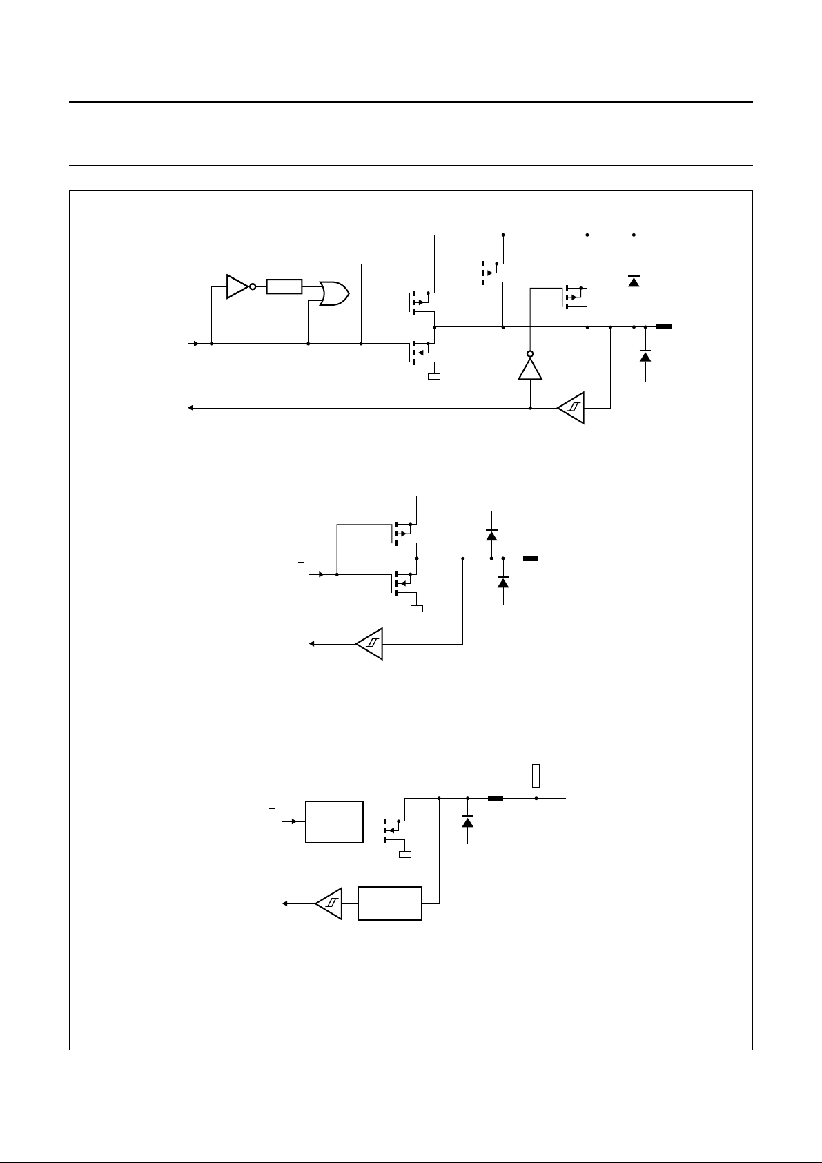
6.6 I/O facilities
6.6.1 P
The PCA5007 has 27 I/O lines treated as 27 individually
addressable bits or as four parallel 8-bit addressable ports.
Ports 0 and 2 are complete, Port 1 has only 7 and Port 3
has only 4 pins externally available. Ports 0, 1, 2 and 3
perform the following alternative functions:
Port 0 Is also used for external access, parallel OTP
Port 1 Used for a number of alternative functions
ORTS
programming mode and emulation (see Table 2 for
configuration details):
• Provides the multiplexed low-order address and
data bus for expanding the device with standard
memories and peripherals
• Provides access to the OTP data I/O lines in OTP
parallel programming mode.
(see Table 3 for configuration details):
• Provides the inputs for the external interrupts
INT2/P1.0 to INT4/P1.2 and INT6/P1.4
• SCL/P1.6 and SDA/P1.7 for the I2C-bus interface
are real open-drain outputs; no other port
configurations are available
• RXD/P1.3 and TXD/P1.4 for the UART data input
and output.
Port 3 Pins are configured as strong push-pull outputs
(see Table 5 for configuration details).
The following alternative Port 3 functions are
available, but to avoid short-circuiting of the port
pins, the input signals cannot be applied externally
to the Port 3 pins. The alternative function can only
be stimulated via the respective port output
function:
• External interrupt request inputs INT0/P3.2 and
INT1/P3.3
• Counter inputs T0/P3.4 and T1/P3.5.
To enable a port pin alternative function, the port bit latch
in its SFR must contain a logic 1.
Each port consists of a latch (SFRs P0 to P3), an output
driver and input buffer. Standard ports have internal
pull-ups. Figure 6a shows that the strong transistor p1 is
turned on for only a short time after a LOW-to-HIGH
transition in the port latch. When on, it turns on p3 (a weak
pull-up) through the inverter IN1. This inverter and p3 form
a latch which holds the logic 1.
6.6.2 P
I/O port output configurations are determined on-chip
according to one of the options illustrated in Fig.6. They
cannot be changed by software.
ORT I/O CONFIGURATION (OPTIONS)
Port 2 Is also used for external access, parallel OTP
programming mode and emulation (see Table 4 for
configuration details):
• Provides the high-order address bus when
expanding the device with external program
memory
• Allows control of the on-chip OTP parallel
programming mode.
1998 Oct 07 15
Page 16
Philips Semiconductors Product specification
Pager baseband controller PCA5007
handbook, full pagewidth
from port latch
input data
handbook, full pagewidth
V
weak pull-up
delay >50 ns
Q
strong pull-up
p1
n
V
SS
p2
hold pull-up
p3
IN1
V
DD
I/O pin
SS
MGR111
a. Standard/quasi-bidirectional (option 1).
V
from port latch
input data
DD
strong pull-up
p1
Q
n
V
SS
V
DD
I/O pin
V
SS
MGR112
b. Push-pull (option 3).
handbook, full pagewidth
from port latch
Q
input data
SLEW
RATE
CONTROL
V
SS
LOW-PASS
FILTER
c. Open-drain (only SDA/P1.7, SCL/P1.6; option 2).
Fig.6 Port configuration options.
1998 Oct 07 16
V
external
DD
I/O pin
n
V
SS
MGR113
external
pull-up
Page 17
Philips Semiconductors Product specification
Pager baseband controller PCA5007
6.6.3 PORT I/O CONFIGURATION
Tables 2 to 6 show the hardwired configuration for the different I/Os of the PCA5007.
Table 2 Port 0 configuration; notes 1 and 2
POSSIBLE
PORT PIN CONFIGURATION PULL-UP INPUT RESET DRIVE
P0.0 quasi bidirectional I/O (option 1S) yes hys HIGH 0.75 mA LCD_enable (O)
P0.1 quasi bidirectional I/O (option 1S) yes hys HIGH 0.75 mA SPI_enable (O)
P0.2 quasi bidirectional I/O (option 1S) yes hys HIGH 0.75 mA SPI_clock (O)
P0.3 quasi bidirectional I/O (option 1S) yes hys HIGH 0.75 mA SPI_data (O)
P0.4 quasi bidirectional I/O (option 1S) yes hys HIGH 0.75 mA SPI_data (I)
P0.5 quasi bidirectional I/O (option 1R) yes hys LOW 0.75 mA RXE (O)
P0.6 quasi bidirectional I/O (option 1R) yes hys LOW 0.75 mA ROE (O)
P0.7 quasi bidirectional I/O (option 1S) yes hys HIGH 0.75 mA bandwidth (O)/RSSI (I)
APPLICATION IN A
PAGER
Notes
1. Option 1S means port configuration option 1 with post-reset set to HIGH; option 1R means post-reset state will be
LOW.
2. ‘hys’ means input stage with hysteresis.
Table 3 Port 1 configuration
POSSIBLE
PORT PIN CONFIGURATION PULL-UP INPUT RESET DRIVE
APPLICATION IN A
PAGER
P1.0 quasi bidirectional I/O (option 1S) yes hys HIGH 0.75 mA Key
P1.1 quasi bidirectional I/O (option 1S) yes hys HIGH 0.75 mA Key
P1.2 quasi bidirectional I/O (option 1S) yes hys HIGH 0.75 mA Key
P1.3 quasi bidirectional I/O (option 1S) yes hys HIGH 0.75 mA RXD
P1.4 quasi bidirectional I/O (option 1S) yes hys HIGH 0.75 mA TXD
P1.5 not available
P1.6 I
2
C-bus open-drain I/O (option 2S)
no hys HIGH 2.25 mA SCL
(slew rate limited)
P1.7 I
C-bus open-drain I/O (option 2S)
no hys HIGH 2.25 mA SDA
2
(slew rate limited)
Table 4 Port 2 configuration
POSSIBLE
PORT PIN CONFIGURATION PULL-UP INPUT RESET DRIVE
APPLICATION IN A
PAGER
P2.0 quasi bidirectional I/O (option 1S) yes hys HIGH 0.75 mA LCD_Data
P2.1 quasi bidirectional I/O (option 1S) yes hys HIGH 0.75 mA LCD_Data
P2.2 quasi bidirectional I/O (option 1S) yes hys HIGH 0.75 mA LCD_Data
P2.3 quasi bidirectional I/O (option 1S) yes hys HIGH 0.75 mA LCD_Data
1998 Oct 07 17
Page 18
Philips Semiconductors Product specification
Pager baseband controller PCA5007
POSSIBLE
PORT PIN CONFIGURATION PULL-UP INPUT RESET DRIVE
P2.4 quasi bidirectional I/O (option 1S) yes hys HIGH 0.75 mA LCD_Data
P2.5 quasi bidirectional I/O (option 1S) yes hys HIGH 0.75 mA LCD_Data
P2.6 quasi bidirectional I/O (option 1S) yes hys HIGH 0.75 mA LCD_Data
P2.7 quasi bidirectional I/O (option 1S) yes hys HIGH 0.75 mA LCD_Data
Table 5 Port 3 configuration
PORT PIN CONFIGURATION PULLUP INPUT RESET DRIVE
P3.0 not available
P3.1 not available
P3.2 push-pull output (option 3R) no hys LOW 3 mA call LED
P3.3 push-pull output (option 3R) no hys LOW 3 mA vibrator
P3.4 push-pull output (option 3R) no hys LOW 3 mA backlight
P3.5 push-pull output (option 3R) no hys LOW 3 mA LCD R/
P3.6 not available
P3.7 not available
APPLICATION IN A
PAGER
POSSIBLE
APPLICATION IN A
PAGER
W/RXD Enable
The port configuration is fixed and cannot be reconfigured by software or ROM code.
Table 6 Other pins
POSSIBLE
PORT PIN CONFIGURATION PULL-UP INPUT RESET DRIVE
AT push-pull output no LOW 3 mA tone generator output
I(D1) digital input no hys
Q(D0) digital input no hys
TCLK digital input no hys
RESETIN digital input no hys reset input
RESOUT push-pull output no LOW 1.5 mA reset output
XTL1 analog input/output (10 pF) no hys to crystal quartz
XTL2 analog input/output (10 pF) no to crystal quartz
AFCOUT analog output no
ALE quasi bidirectional I/O yes hys HIGH 1.5 mA
PSEN quasi bidirectional I/O yes hys HIGH 0.75 mA
EA 3-state I/O with bus keeper hold buffer HIGH 0.75 mA
APPLICATION IN A
PAGER
1998 Oct 07 18
Page 19
Philips Semiconductors Product specification
Pager baseband controller PCA5007
6.7 Timer/event counters
The PCA5007 contains two 16-bit timer/event counters,
Timer 0 and Timer 1, which can perform the following
functions:
• Measure time intervals and pulse durations
• Count events
• Generate interrupt requests
• Generate output on comparator match
• Generate a Pulse Width Modulated (PWM) output
signal.
Timer 0 and Timer 1 can be programmed independently to
operate in four modes:
Mode 0: 8-bit timer or 8-bit counter each with
divide-by-32 prescaler
Mode 1: 16-bit time interval or event counter
Mode 2: 8-bit time interval or event counter with
automatic reload upon overflow
Mode 3: this mode of the standard 80C51 is not
available.
In the timer mode the timers count events on the XTL1
input. Timer 0 counts through a prescaler at a rate of
256 Hz and Timer 1 counts directly on both edges of the
XTL1 signal at a rate of 153.6 kHz. The nominal frequency
of the XTL1 signal is 76.8 kHz.
In the counter mode, the register is incremented in
response to a HIGH-to-LOW transition at P3.4 (T0) and
P3.5 (T1).
Besides the different input frequencies and the
non-availability of Mode 3, both Timer 0 and Timer 1
behave identically to the standard 80C51 Timer 0 and
Timer 1.
handbook, full pagewidth
Detailed configuration of the 4 available modes is found in the 80C51 family hardware description (
XTL1
T0
Gate
INT0
XTL1
T1
Gate
INT1
÷ 300
256 Hz
C/T = 0
C/T = 1
TR0
153.6 kHz
C/T = 0
C/T = 1
TR1
Fig.7 Timer/counter 0 and 1: clock sources and control logic.
TL0
TL1 TH1
“Philips Semiconductors IC20 Data Handbook”
TH0
MGR114
).
1998 Oct 07 19
Page 20

Philips Semiconductors Product specification
Pager baseband controller PCA5007
6.8 I2C-bus serial I/O
The serial port supports the 2-line I2C-bus which consists
of a data line (SDA) and a clock line (SCL). These lines
also function as the I/O port lines P1.7 and P1.6
respectively. The system is unique because data
transport, clock generation, address recognition and bus
control arbitration are all controlled by hardware.
The I2C-bus serial I/O has complete autonomy in byte
handling. The implementation in the PCA5007 operates in
single master mode as:
• Master transmitter
• Master receiver.
These functions are controlled by the S1CON register.
S1STA is the status register whose contents may also be
used as a vector to various service routines. S1DAT is the
data shift register. The block diagram of the I2C-bus
serial I/O is shown in Fig.8.
6.8.1 DIFFERENCES TO A STANDARD I2C-BUS INTERFACE
The I2C-bus interface of the PCA5007 implements the
standard for master receiver and transmitter as defined in
e.g. P83CL781/782 with the following restrictions:
• The baud rate is fixed to 100 kHz derived from the
on-chip 6 MHz oscillator. Therefore bits CR0, CR1 and
CR2 in the S1CON SFR are not available.
• Only single master functions are implemented.
– Slave address (S1ADR) is not available
– Status register (S1STA) reports only status defined
for the MST/TRX and MST/REC modes
– Multimaster operation is not supported.
handbook, full pagewidth
SDA
ARBITRATION LOGIC
SCL BUS CLOCK GENERATOR
76543210
S1CON
76543210
S1STA
SHIFT REGISTER
S1DAT
Fig.8 Block diagram of I2C-bus serial I/O.
INTERNAL BUS
MGL449
1998 Oct 07 20
Page 21

Philips Semiconductors Product specification
Pager baseband controller PCA5007
6.8.2 SERIAL CONTROL REGISTER (S1CON)
Table 7 Serial Control Register (S1CON, SFR address D8H)
76543210
−ENS1 STA STO SI AA −−
Table 8 Description of the S1CON bits
BIT SYMBOL FUNCTION
S1CON.7 − CR2 is not available.
S1CON.6 ENS1 Enable Serial I/O. When ENS1 = 0, the serial I/O is disabled. SDA and SCL outputs are
in the high-impedance state; P1.6 and P1.7 function as open-drain ports. When
ENS1 = 1, the serial I/O is enabled. Output port latches P1.6 and P1.7 must be set to
logic 1.
S1CON.5 STA START flag. If STA is set while the SIO is in master mode, SIO will generate a repeated
START condition.
S1CON.4 STO STOP flag. With this bit set while in master mode a STOP condition is generated. When
a STOP condition is detected on the I
S1CON.3 SI SIO interrupt flag. This flag is set, and an interrupt is generated, after any of the
following events occur:
• A START condition is generated in master mode
• A data byte has been received or transmitted in master mode (even if arbitration is lost).
If this flag is set, the I
2
C-bus is halted (by pulling down SCL). Received data is only valid
until this flag is reset.
S1CON.2 AA Assert Acknowledge. When this bit is set, an acknowledge (LOW level to SDA) is
returned during the acknowledge clock pulse on the SCL line when:
• A data byte is received while the device is programmed to be a master receiver.
When this bit is reset, no acknowledge is returned.
S1CON.1 − CR1 and CR0 are not available.
S1CON.0 −
2
C-bus, the SIO hardware clears the STO flag.
6.8.3 D
ATA SHIFT REGISTER (S1DAT)
S1DAT contains the serial data to be transmitted or data which has just been received. Bit 7 is transmitted or received
first; i.e. data shifted from left to right.
Table 9 Data Shift Register (S1DAT, SFR address DAH)
76543210
D7 D6 D5 D4 D3 D2 D1 D0
6.8.4 A
DDRESS REGISTER (S1ADR)
The slave address register is not available since slave mode is not supported.
6.8.5 S
ERIAL STATUS REGISTER (S1STA)
The contents of this register may be used as a vector to a service routine. This optimizes the response time of the
software and consequently that of the I2C-bus. S1STA is a read-only register. The status codes for all available modes
of a single master I2C-bus interface are given in Tables 12 to 14.
1998 Oct 07 21
Page 22
Philips Semiconductors Product specification
Pager baseband controller PCA5007
Table 10 Serial Status Register (S1STA and SFR address D9H)
76543210
SC4 SC3 SC2 SC1 SC0 0 0 0
Table 11 Description of the S1STA bits
BIT SYMBOL FUNCTION
S1STA.3 to S1STA.7 SC4 to SC0 5-bit status code
S1STA.0 to S1STA.2 − these 3 bits are held LOW
Table 12 MST/TRX mode
S1STA VALUE DESCRIPTION
08H a START condition has been transmitted
10H a repeated START condition has been transmitted
18H SLA and W have been transmitted, ACK has been received
20H SLA and W have been transmitted,
28H DATA of S1DAT has been transmitted, ACK received
30H DATA of S1DAT has been transmitted,
ACK received
ACK received
Table 13 MST/REC mode
S1STA VALUE DESCRIPTION
40H SLA and R have been transmitted, ACK received
48H SLA and R have been transmitted,
50H DATA has been received, ACK returned
58H DATA has been received,
Table 14 Miscellaneous
S1STA VALUE DESCRIPTION
78H no information available (reset value); the serial interrupt flag SI, is not yet set
Table 15 Symbols used in Tables 12 to 14
SYMBOL DESCRIPTION
SLA 7-bit slave address
R read bit
W write bit
ACK acknowledgement (acknowledge bit = logic 0)
ACK no acknowledgement (acknowledge bit = logic 1)
DATA 8-bit data byte to or from I
MST master
SLV slave
TRX transmitter
REC receiver
ACK returned
2
C-bus
ACK received
1998 Oct 07 22
Page 23

Philips Semiconductors Product specification
Pager baseband controller PCA5007
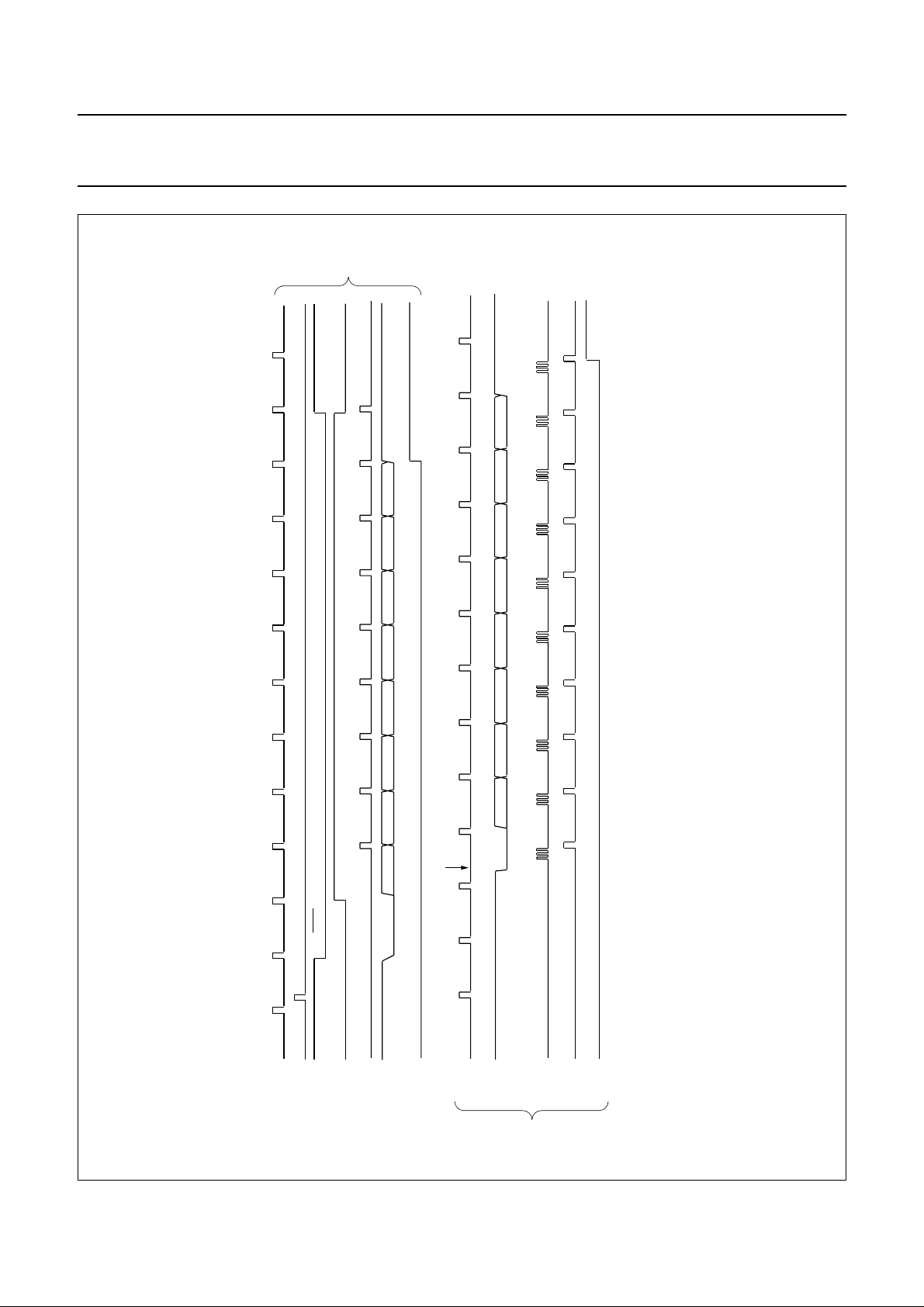
6.9 Serial interface SIO0: UART
The UART interface of the PCA5007 implements a subset
of the complete standard as defined in e.g. the P80CL580.
6.9.1 D
IFFERENCES TO THE STANDARD 80C51 UART
The following deviations from the standard exist:
• If [SM1 and SM0] = 10 then Mode 1 (8-bit data
transmission) is selected, with a fixed baud rate
(4800/9600 bits/s)
• If [SM1 and SM0] = 01 then Mode 2 (9-bit data
transmission) is selected, with a fixed baud rate
(4800/9600 bits/s)
• Modes 0 and 3 and the variable baud rate selection
using Timer 1 overflow is not available
• The SM2 bit has no function
• The time reference for Modes 1 and 2 is taken from the
f
76.8 kHz oscillator, instead of the original
6.9.2 UART
MODES
OSC
----------12
This serial port is full duplex which means that it can
transmit and receive simultaneously. It is also
receive-buffered and can commence reception of a
second byte before a previously received byte has been
read from the register. However, if the first byte has not
been read by the time the reception of the second byte is
complete, the second byte will be lost. The serial port
receive and transmit registers are both accessed via the
special function register S0BUF. Writing to S0BUF loads
the transmit register and reading from S0BUF accesses a
physically separate receive register.
The serial port can operate in 2 modes:
Mode 1 10 bits are transmitted (through TXD) or received
(through RXD): a START bit (0), 8 data bits (LSB
first) and a STOP bit (1). On receive, the stop bit
goes into RB8 in special function register S0CON
(see Figs 9 and 10).
Mode 2 11 bits are transmitted (through TXD) or received
(through RXD): a START bit (0), 8 data bits (LSB
first), a programmable 9th data bit and a STOP
bit (1). On transmit, the 9th data bit (TB8 in
S0CON) can be assigned the value of 0 or 1.
Or, for example, the parity bit (P, in the PSW)
could be moved into TB8. On receive, the
9th data bit goes into RB8 in S0CON, while the
STOP bit is ignored (see Figs 9 and 11).
In both modes the baud rate can be selected to either
4800 or 9600 depending on the SMOD bit in the PCON
SFR. If SMOD = 0 the baud rate is 4800, if SMOD = 1 the
baud rate is 9600 with a 76.8 kHz quartz crystal.
In both modes, transmission is initiated by any instruction
that uses S0BUF as a destination register. Reception is
initiated by the incoming start bit if REN = 1.
6.9.3 S
ERIAL PORT CONTROL REGISTER (S0CON)
The serial port control and status register is the special
function register S0CON (see Table 16). The register
contains not only the mode selection bits, but also the
9th data bit for transmit and receive (TB8 and RB8), and
the serial port interrupt bits (TI and RI).
Table 16 Serial Port Control Register (S0CON, SFR address 98H)
76543210
SM0 SM1 − REN TB8 RB8 TI RI
1998 Oct 07 23
Page 24
Philips Semiconductors Product specification
Pager baseband controller PCA5007
Table 17 Description of the S0CON bits
BIT SYMBOL FUNCTION
S0CON.7 SM0 this bit together with the SM1 bit, is used to select the serial port mode; see Table 18
S0CON.6 SM1 this bit together with the SM0 bit, is used to select the serial port mode; see Table 18
S0CON.5 − SM2 is not available
S0CON.4 REN this bit enables serial reception and is set by software to enable reception, and cleared by
software to disable reception
S0CON.3 TB8 this bit is the 9th data bit that will be transmitted in Mode 2; set or cleared by software as
desired
S0CON.2 RB8 in Mode 2, this bit is the 9th data bit received; in Mode 1 it is the stop bit that was received
S0CON.1 TI The transmit interrupt flag; Set by hardware at the end of the 8th bit time in Mode 0, or at
the beginning of the stop bit time in the other modes, in any serial transmission; must be
cleared by software.
S0CON.0 RI The receive interrupt flag; Set by hardware at the end of the 8th bit time in Mode 0, or
halfway through the stop bit time in the other modes, in any serial transmission (for exception
see SM2); must be cleared by software.
Table 18 Selection of the serial port modes
SM0 SM1 MODE DESCRIPTION BAUD RATE
0 1 1 8-bit UART
1 0 2 9-bit UART
6.9.4 UART
DATA REGISTER (S0BUF)
1
⁄16f
or1⁄8f
osc
1
⁄16f
osc
or1⁄8f
osc
osc
The UART data register (S0BUF) contains the serial data to be transmitted or data which has just been received. Bit 0
is transmitted or received first.
Table 19 Data Shift Register (S0BUF, SFR address 99H)
76543210
D7 D6 D5 D4 D3 D2 D1 D0
6.9.5 B
AUD RATES
The baud rate in Modes 1 and 2 depends on the value of the SMOD bit in SFR PCON and may be calculated as:
SMOD
Baud rate
2
---------------- -
• If SMOD = 0, (which is the value on reset), the baud rate is
• If SMOD = 1, the baud rate is1⁄8f
16
f
×=
osc
1
⁄16f
osc
.
osc
1998 Oct 07 24
Page 25
Philips Semiconductors Product specification
Pager baseband controller PCA5007
handbook, full pagewidth
CSMOD at
PCON.7
XTL1
2
INTERNAL BUS
TB8
write to
SBUF
S
D
Q
CL
0
1
serial port
interrupt
sample
HIGH-TO-LOW
TRANSITION
DETECTOR
8
ZERO DETECTOR
STOP BIT SHIFT
START
TX CLOCK SEND
8
START
S0 BUFFER
TX CONTROL
T1
RX CLOCK R1
RX CONTROL
SHIFT
DATA
LOAD
SBUF
SHIFT
TXD
BIT
DETECTOR
RXD
Fig.9 Serial port Mode 1and Mode 2.
1998 Oct 07 25
INPUT SHIFT
LOAD
SBUF
READ
SBUF
INTERNAL BUS
REGISTER
(9-BITS)
S0 BUFFER
SHIFT
MGL452
Page 26
Philips Semiconductors Product specification
Pager baseband controller PCA5007
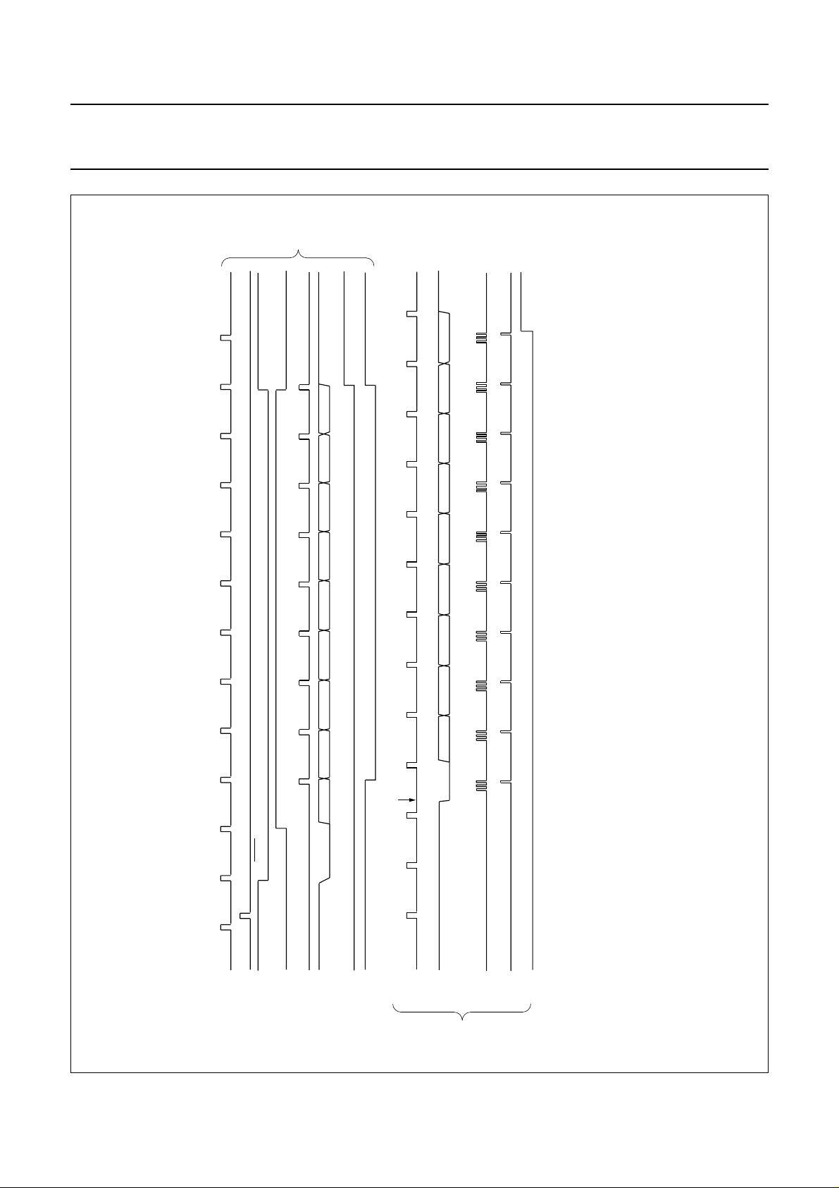
T
RAN
I
T
S
M
MGL451
STOP BIT
STOP BIT
D7
D6
D4 D5
D3
D6 D7
handbook, full pagewidth
This text is here in white to force landscape pages to be rotated correctly when browsing through the pdf in the Acrobat reader.This text is here in
_white to force landscape pages to be rotated correctly when browsing through the pdf in the Acrobat reader.This text is here inThis text is here in
white to force landscape pages to be rotated correctly when browsing through the pdf in the Acrobat reader. white to force landscape pages to be ...
1998 Oct 07 26
WRITE TO SBUF
TX CLOCK
SEND
DATA
SHIFT
D2
D1
D0
START BIT
TXD
TI
÷8 RESET
RX CLOCK
D0 D1 D2 D3 D4 D5
START BIT
RXD
REC
BIT DETECTOR SAMPLE TIME
SHIFT
RI
EIV
E
Fig.10 Serial port Mode 1 timing.
Page 27
Philips Semiconductors Product specification
Pager baseband controller PCA5007
T
RAN
S
I
M
STOP BIT
D7 TB8
D3 D4 D5 D6
T
STOP BIT
RB8
MGL450
handbook, full pagewidth
This text is here in white to force landscape pages to be rotated correctly when browsing through the pdf in the Acrobat reader.This text is here in
_white to force landscape pages to be rotated correctly when browsing through the pdf in the Acrobat reader.This text is here inThis text is here in
white to force landscape pages to be rotated correctly when browsing through the pdf in the Acrobat reader. white to force landscape pages to be ...
1998 Oct 07 27
SEND
WRITE TO SBUF
TX CLOCK
DATA
SHIFT
D0 D1 D2
START BIT
TXD
TI
÷8 RESET
RX CLOCK
STOP BIT GEN
D0 D1 D2 D3 D4 D5 D6 D7
START BIT
RXD
EIV
REC
BIT DETECTOR SAMPLE TIME
SHIFT
RI
E
Fig.11 Serial port Mode 2 timing.
Page 28
Philips Semiconductors Product specification
Pager baseband controller PCA5007
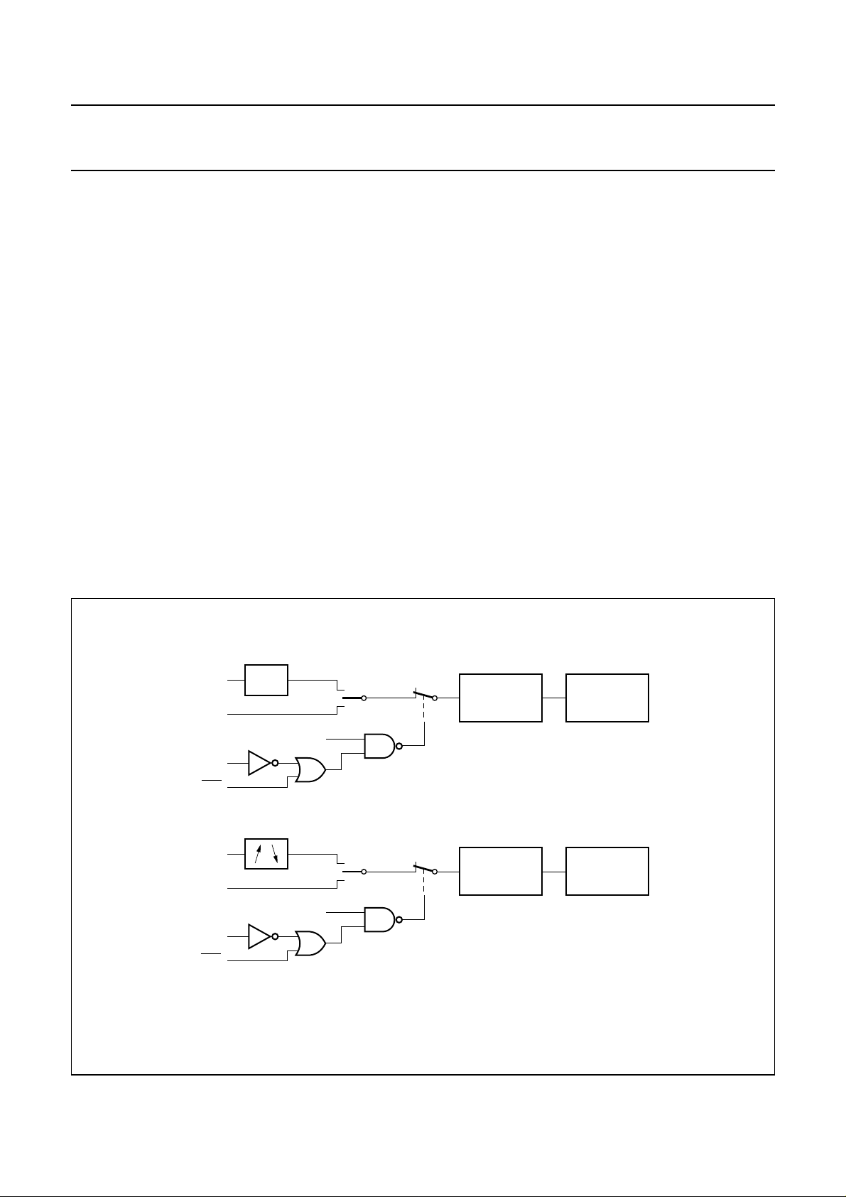
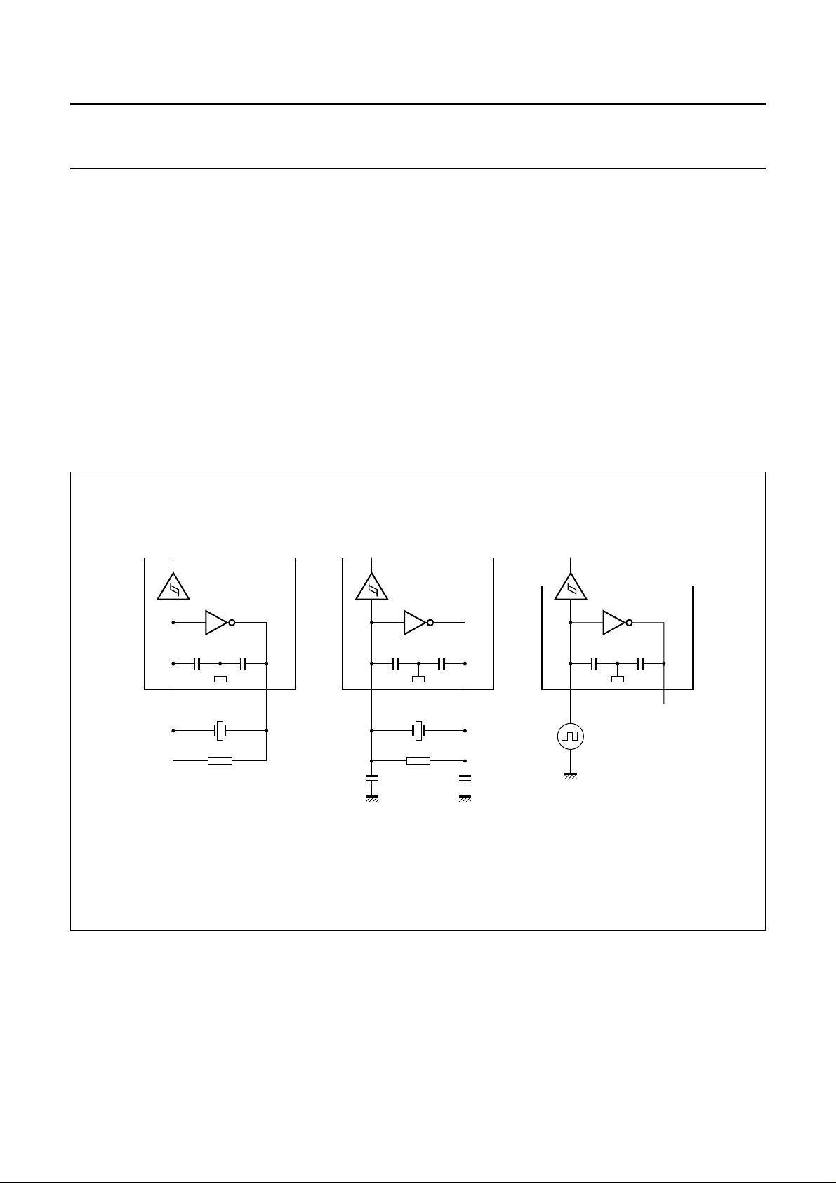
6.10 76.8 kHz oscillator
6.10.1 F
UNCTION
The oscillator produces a reference frequency of 76.8 kHz.
The frequency offset is compensated for by a separate
digital clock correction block. The oscillator operates
directly on V
6.10.2 O
and is always enabled.
BAT
SCILLATOR CIRCUITRY
The on-chip inverting oscillator amplifier is a single NMOS
transistor supplied with a constant current. The amplitude
visible at terminals XTL1 and XTL2 is therefore not a full
rail swing with a very high impedance. To reduce the
power consumption, the input Schmitt trigger buffer is
limited to approximately 100 kHz maximum frequency.
handbook, full pagewidth
76.8 kHz 76.8 kHz 76.8 kHz
The whole circuit operates directly at the battery supply.
The 76.8 kHz oscillator cannot be disabled. It also
continues its operation during DC/DC converter off or
8051 stop mode.
The simplest application configuration is shown in Fig.12a.
C1 and C2 can be added to operate a crystal at its
optimum load condition. The resulting capacitance of the
series connection of C1 and C2 must be smaller than 5 pF
for a guaranteed start-up of the oscillator.
10 pF
XTL1 XTL2
10 pF
XTL1 XTL2
76.8 kHz
2 MΩ
C1
(a) (b) (c)
10 pF10 pF
76.8 kHz
2 MΩ
C2
Fig.12 Oscillator circuit.
10 pF10 pF
XTL1 XTL2
VP = V
BAT
f
= 100 kHz
max
MGR115
1998 Oct 07 28
Page 29
Philips Semiconductors Product specification
Pager baseband controller PCA5007
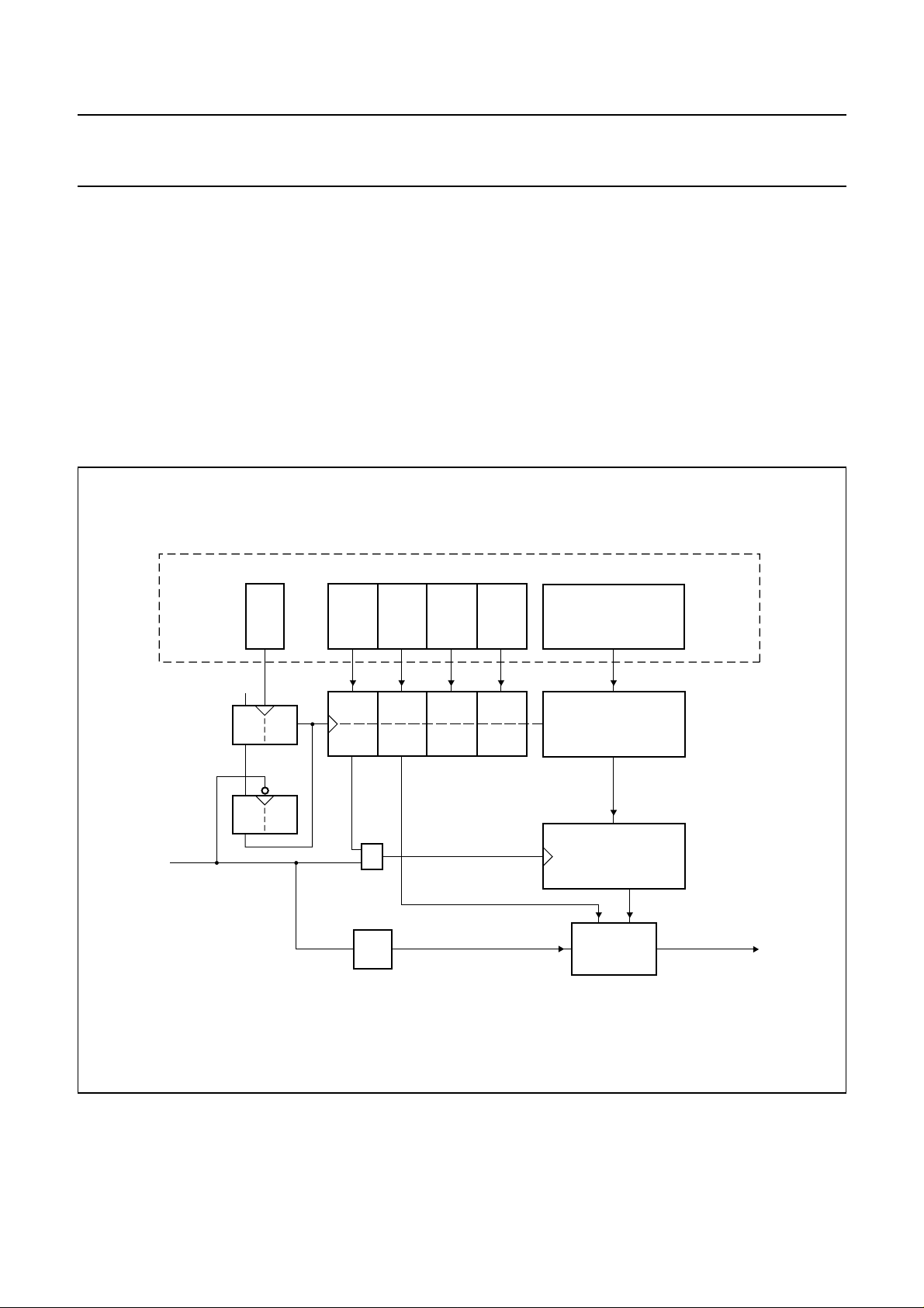
6.11 Clock correction
6.11.1 F
UNCTION
The clock correction block is connected to the 76.8 kHz
oscillator. It operates directly from V
. By means of the
BAT
clock correction circuit a digital adjustment of the 76.8 kHz
oscillator signal is implemented.
An 18-bit interval counter inserts or deletes one pulse from
the 76.8 kHz clock each time its count has expired.
The interval is stored by the processor to the 18-bit interval
register CIV. Addition or deletion is performed by
hardware.
handbook, full pagewidth
SFR to
microcontroller
SET ENB PLUS
BYPASS TEST
Crystal offset correction can be performed with a
resolution of 5 ppm.
This block also generates the timing reference signals for
other functional blocks such as the RTC (4 Hz), watchdog
(16 Hz), Timer 0 (256 Hz), wake-up counter (9600 Hz)
and the demodulator/clock recovery block. The generation
of these timing references is always active and cannot be
disabled.
VDD supply
CIV0 to CIV17
RESET
with each
OFF cycle
76.8 kHz
internal
set flag
1
D
QD Q
R
STORE
RESET only
on RESETIN
&
÷2
V
supply
BAT
Fig.13 Block diagram for clock compensation.
INTERVAL LATCH
(18-BIT)
reload data
INTERVAL COUNTER
(18-BIT)
(RELOAD ON CARRY)
CARRY
ADD/DELETE
ONE PULSE
ON CARRY
corrected
38.4 kHz
MGR116
1998 Oct 07 29
Page 30
Philips Semiconductors Product specification
Pager baseband controller PCA5007
6.11.2 CLOCK CORRECTION CONTROL REGISTER (CCON)
The CCON special function register is used to control the clock correction by software.
Table 20 Clock Correction Control Register (CCON, SFR address FCH)
76543210
ENB PLUS TEST CIV17 CIV16 −
Table 21 Description of the CCON bits
BIT SYMBOL FUNCTION
CCON.7 ENB Enable clock correction. If ENB = 1 has been set, then correction is enabled and will
stay enabled even when the DC/DC converter is shut down and restarted.
CCON.6 PLUS ± sign for value. If PLUS = 1 then clock pulses are inserted, or else deleted.
CCON.5 TEST Test signal, must always be logic 0 in normal mode. It is s used during test to bypass
the first 9 FFs in the timing generator divider chain. If TEST = 1 the clock rate of the
signals 9600 Hz and 256 Hz is doubled and the frequency on 16 Hz and 4 Hz is
multiplied by 300.
CCON.4 CIV17 bit 17 of interval value, is used as extension of CC0 and CC1
CCON.3 CIV16 bit 16 of interval value, is used as extension of CC0 and CC1
CCON.2 − unused.
CCON.1 BYPASS Test signal, must always be logic 0 in normal mode. It is used during test to generate
76.8 kHz on all outputs of the timing generator (4 Hz, 16 Hz, 256 Hz and 9600 Hz).
CCON.0 SET A load signal to the interval register. After a logic 0 to logic 1 transition of this bit the
value of ENB, PLUS, TEST, BYPASS and CIV are copied into the local latches with the
next 76.8 kHz clock pulse. The duration of one MOV instruction is long enough for the
set operation to complete. The SFR values must remain stable for at least one oscillator
period because the actual transfer happens synchronized with the local clock
(see Figs 14 and 16).
BYPASS
SET
6.11.3 C
The CC0 and CC1 special function registers (together with CCON.3 and CCON.4) are used to define the interval between
subsequent clock correction actions.
Table 22 Clock Correction Interval Register (CC0, SFR address FDH)
Table 23 Clock Correction Interval Register (CC1, SFR address FEH)
1998 Oct 07 30
LOCK CORRECTION INTERVAL REGISTERS (CC0 AND CC1)
76543210
CIV7 CIV6 CIV5 CIV4 CIV3 CIV2 CIV1 CIV0
76543210
CIV15 CIV14 CIV13 CIV12 CIV11 CIV10 CIV9 CIV8
Page 31

Philips Semiconductors Product specification
Pager baseband controller PCA5007
6.11.4 EXAMPLE SEQUENCE TO SET ANOTHER CLOCK CORRECTION INTERVAL
handbook, full pagewidth
PLUS, ENB
and CIV
SET
valid value in SFR
must stay valid for
one period of 76.8 kHz
MGR117
Fig.14 Sequence for setting the clock compensation.
MOV CC0, #(CIV7 to CIV0).
MOV CC1, #(CIV8 to CIV15).
MOV CCON, #D4H.
MOV CCON, #D5H.
6.11.5 T
IMING
Figures 15 and 16 illustrate how the clock correction works and how the access of the microcontroller is synchronized to
the local operation.
handbook, full pagewidth
Interval counter
[CIV] − 3
[CIV] − 2
[CIV] − 1
[CIV]
0
1
2
3
4
5
6
76.8 kHz
38.4 kHz
CORR for
clock recovery
corrected
38.4 kHz
with PLUS = 1
corrected
38.4 kHz
with PLUS = 0
After (CIV) clock ticks of 76.8 kHz or 38.4 kHz one correction is made.
Fig.15 Operation of clock compensation.
1998 Oct 07 31
[CIV] − 5
[CIV] − 4
[CIV] − 3
[CIV] − 2
[CIV] − 1
[CIV]
0
1
2
3
4
5
6
7
[CIV] − 5
[CIV] − 4
MGR118
Page 32

Philips Semiconductors Product specification
Pager baseband controller PCA5007
SET (SFR)
handbook, full pagewidth
SET flag (local)
76.8 kHz
store (local)
data (SFR)
data (local)
reload from
local data
counter
I I − 1 I − 2 I − 3 I − 4 1 0 K K − 1 K − 2
Fig.16 Synchronization of local counter operation and access from the microcontroller.
6.12 6 MHz oscillator
6.12.1 F
UNCTION
The 6 MHz oscillator provides the clock for the DC/DC
converter, the I2C-bus interface, the port I/Os and for the
external memory access timing (ALE/PSEN).
The 6 MHz oscillator is a 5 inverter stage current
controlled ring oscillator. The oscillator is optimized for low
operating current consumption.
The actual frequency of the oscillator can be measured by
activating the MFR signal. An 8-bit counter will then be
reset and will start counting at the first rising edge of the
76.8 kHz signal and will stop counting at the next rising
edge of the 76.8 kHz signal. The processor then can read
the contents of the MFR counter.
The processor can adjust the oscillator frequency using
the F0 to F4 signals (control of source current for ring
oscillator).
The 6 MHz oscillator is enabled by hardware only during
the start-up phase and whenever the DC/DC converter
needs the 6 MHz clock. In all other cases the 6 MHz
oscillator is switched off by hardware.
K
K
MGR119
The DC/DC converter does not need the 6 MHz clock
when set in the standby mode.
If the 6 MHz output is required as a frequency source for
other blocks (e.g. I
2
C-bus) the software needs to enable it
explicitly by setting ENB = 1. Besides the DC/DC
converter the following functions require the operation of
the 6 MHz oscillator:
• I2C-bus block as basic time reference
• Port output logic. Software commands that write to the
ports need this clock to complete the operation (if a
program ‘hangs’, this could be the problem).
• Code fetching from external memories needs the clock
for the ALE/PSEN timing (e.g. LJMP 5000H needs this
clock for completion).
When the ENB bit has been set by software, the clock will
be available internally after the start-up time of this
oscillator. The start-up time is 2 to 3 periods of the
76.8 kHz reference frequency.
1998 Oct 07 32
Page 33

Philips Semiconductors Product specification
Pager baseband controller PCA5007
6.12.2 6 MHZ OSCILLATOR CONTROL REGISTER (OS6CON)
The OS6CON special function register is used to control the operation of the on-chip 6 MHz oscillator. The 6 MHz
oscillator can be controlled as follows:
• It can be enabled or disabled. Disabling this oscillator when the DC/DC converter is in standby mode and no port I/O
nor I2C-bus activity is required saves current.
• The frequency of the oscillator can be adjusted by setting the SFx bits accordingly
• The actual frequency of the oscillator can be measured by writing the MFR bit to logic 1.
Table 24 6 MHz Oscillator Control Register (OS6CON, SFR address D3H)
76543210
ENB −
Table 25 Description of the OS6CON bits
BIT SYMBOL FUNCTION
OS6CON.7 ENB Enable oscillator. If ENB = 1 then the function is enabled. The enable bit is only
OS6CON.6 − unused
OS6CON.5 SF4 Set frequency. This 5-bit value adjusts the current of the ring oscillator and thus the
OS6CON.4 SF3
OS6CON.3 SF2
OS6CON.2 SF1
OS6CON.1 SF0
OS6CON.0 MFR Measure frequency. If a positive pulse is issued on this SFR-bit a frequency
SF4 SF3 SF2 SF1 SF0 MFR
cleared when the processor writes the bit to logic 0, or if the DC/DC converter is put into
‘OFF’ state and a reset is generated during the following power-up sequence.
frequency. Writing a small value decreases the frequency. The nominal frequency of
6 MHz is assigned to code (SF4, SF3, SF2, SF1 SF0) = 00000. The resolution of the
frequency adjustment is 200 kHz per step, the range is approximately 3 to 9 MHz.
In order to start with the nominal frequency the MSB bit is inverted in this SFR.
measurement cycle is executed. The duration of this cycle is one period of 76.8 kHz.
The count of 6 MHz periods during the measurement cycle is reported back in OS6M0.
The bit must be reset by software.
6.12.3 6 MH
The actual frequency of the 6 MHz on-chip oscillator can be calculated from the value in the OS6M0 special function
register, after a Measure Frequency operation (MFR).
Table 26 6 MHz Oscillator Measured Frequency Register (OS6M0, SFR address D4H)
76543210
MF7 MF6 MF5 MF4 MF3 MF2 MF1 MF0
The value stored in this SFR is the counted number of 6 MHz cycles during one 76.8 kHz period. The frequency of the
6 MHz oscillator is therefore f = MF × 76800 Hz with a resolution of 76800 Hz.
1998 Oct 07 33
Z OSCILLATOR MEASURED FREQUENCY REGISTER (OS6M0)
Page 34

Philips Semiconductors Product specification
Pager baseband controller PCA5007
6.12.4 ENABLING OF THE 6MHZ OSCILLATOR
handbook, full pagewidth
MICROCONTROLLER
DC/DC CONVERTER
S0CON,
S0BUF
OS6CON,
ENB
ENB
SERIAL INTERFACE
≥ 1
Fig.17 Relationship between 6 MHz oscillator, DC/DC converter and microcontroller.
6.13 Real-time clock
6.13.1 F
UNCTION
The Real-Time Clock (RTC) consists of an 8-bit counter
that is active at all times. To save power it is operated
directly on V
. It counts up on every 4 Hz clock pulse
BAT
(corrected clock).
The RTC can be read from and written to by the processor.
When it reaches 239, the signal MINUTE is activated. This
signal resets the counter to 0 (at the next clock pulse), and
generates a MIN-interrupt for the processor.
The microcontroller ‘sees’ the minute interrupt as if it was
an X9 interrupt. It can be enabled and disabled and must
be cleared as an X9 interrupt (CLR IQ9).
I2C-BUS
&
6 MHz OSCILLATOR
ENB F6M
PX
PORT I/O
EXTERNAL ACCESS
MGR120
If the DC/DC converter is not active when this happens,
the DC/DC converter is started first, and a
power-up/restart sequence of the microcontroller follows.
The MIN bit remains set during this procedure.
6.13.2 R
EAL-TIME CLOCK CONTROL REGISTER (RTCON)
The RTCCON special function register is used to control
the operation of the on-chip real-time clock function.
1998 Oct 07 34
Page 35

Philips Semiconductors Product specification
Pager baseband controller PCA5007
Table 27 RTC Control Register (RTCCON, SFR address CDH)
76543210
MIN −−−−W/
Table 28 Description of the RTCON bits
BIT SYMBOL FUNCTION
RTCON.7 MIN MIN is activated when the counter reaches 239. MIN is used to generate the interrupt
request signal MINUTE. In order to complete the interrupt cycle and reset the interrupt
source, the processor has to clear MIN. This must be done in a 2 step operation writing
MIN and then applying a positive edge to SET.
RTCON.6 − unused
RTCON.5 − unused
RTCON.4 − unused
RTCON.3 − unused
RTCON.2 W/
RTCON.1 LOAD Load RTC with contents of RTC0. LOAD is sampled with the positive edge of the set
RTCON.0 SET Latch signal for the real-time clock. With the pulse on SET the content of MIN is
R Before the RTC time can be set by software, the updating of the SFR by the RTC must
be disabled. This is done by writing the W/R bit to logic 1. The W/R bit is cleared by
hardware after the next 4 Hz clock, when the RTC has been loaded with its next value.
flag SET. If LOAD is not HIGH during a SET operation, only the MIN flag is (re)set by the
command.
copied into the ‘real’ MIN latch. This is necessary because the RTC has to be active at
all times independant of the microcontroller.
R LOAD SET
6.13.3 R
Table 29 RTC Data Register (RTC0, SFR address CEH)
QSECS7 QSECS6 QSECS5 QSECS4 QSECS3 QSECS2 QSECS1 QSECS0
The value stored in this SFR is the actual 4 Hz count since the last MINUTE interrupt. The contents of this counter can
be read from and written to by software. The contents of this counter are only initialized when RESETIN is activated.
During an OFF sequence, the RTC continues its operation.
The value of the RTC data register is only updated while the STB flag in the DCCON0 SFR is HIGH, i.e. the DC/DC
converter is able to sustain the VDD supply voltage. If the STB flag is at logic 0 the real-time clock continues its operation,
the MINUTE interrupt occurs regularly, but the SFR is not updated.
EAL-TIME CLOCK DATA REGISTER (RTC0)
76543210
1998 Oct 07 35
Page 36

Philips Semiconductors Product specification
Pager baseband controller PCA5007
6.13.4 EXAMPLE SEQUENCE FOR PROGRAMMING THE RTC:
Sequence to set another value into the RTC:
MOV RTCON, #06H; set LOAD, W/R bits
MOV RTC0, #(new value); load new RTC value into
SFR
MOV RTCON, #07H; now set the data valid flag (SET)
in the SFR.
handbook, full pagewidth
4 Hz
data (RTC0)
W/R (RTCON)
update by
hardware
imi + 1
MOV RTC0 #m
MOV RTCON #...
Sequence to clear an interrupt of the RTC:
CLR IQ9; Interrupt request flag is IQ9
MOV RTCON, #00H; clear also MIN flag in the SFR
MOV RTCON, #01H; now set the data valid flag (SET)
in the SFR.
6.13.5 TIMING
The interface between 2 and 1 V regions is implemented
similar to the clock correction block. The sequence for
writing values is identical (see Fig.13).
data must be valid until here
cleared by hardware
update by
hardware
m + 1
LOAD (RTCON)
SET (RTCON)
internal SET flag
internal store
internal write
RTC value
ii + 1
Fig.18 Operation of RTC to microcontroller interface.
mm + 1
MGR121
1998 Oct 07 36
Page 37

Philips Semiconductors Product specification
Pager baseband controller PCA5007
6.14 Wake-up counter
6.14.1 F
UNCTION
The wake-up counter is intended to be used as a protocol
timer. It can be programmed to wake-up the processor
when the protocol needs an action. Amongst others this
may be:
• Switching on the DC/DC converter at time 0
• Enabling the receiver at time 1
• Enabling the demodulator and clock recovery function
at time 2 before relevant data is expected.
The time to wake-up is defined as a 16-bit value containing
the number of 9600 Hz ticks. The maximum time interval
that can be spawn with one cycle then equals 6.8 s.
The wake-up counter and its reload latch are supplied by
V
and operate independent of the 2 V supply.
BAT
A reset to the microcontroller does not clear the wake-up
counter control flags or the reload latch, but clears the
reload register (see Fig.19).
The counter is implemented as a 16-bit ripple-down
counter. It can be loaded from the wake-up reload latch by
a signal from the processor. When the counter is loaded it
automatically starts if the RUN signal is active. When the
counter reaches zero the wake-up signal becomes active
and may generate an interrupt. The wake-up signal
automatically reloads the counter (modulo N counter).
The counter is stopped when the RUN signal is written to
logic 0. Auto reloading of the counter is also possible,
when the DC/DC converter is not operating (i.e. V
DD
is
below 1.8 V).
The contents of the wake-up counter cannot be read by the
processor. Reading WUC0 and WUC1 reflects the
contents of the 16-bit wake-up register (set by the
microcontroller).
The interface between the 2 and 1 V regions is
implemented similar to the clock correction block.
The sequence for writing values is identical (see Fig.14).
handbook, full pagewidth
Interrupt
microcontroller
internal
SET FLAG
9600 Hz
SFR to
1
D
QD Q
≥ 1
SET
CPL
R
STORE
RUN LOAD WUP
&
TEST
≥ 1
VDD supply
Z1 Z0
reload
V
BAT
WU RELOAD LATCH
RESET only
on RESETIN
supply
WU0 to WU15
wake-up DC/DC converter
(16-BIT)
reload data
WU COUNTER
(16-BIT)
RESET
with each
OFF cycle
CARRY
MGR122
Fig.19 Block diagram of the wake-up counter.
1998 Oct 07 37
Page 38

Philips Semiconductors Product specification
Pager baseband controller PCA5007
6.14.2 WAKE-UP COUNTER CONTROL REGISTER (WUCON)
The WUCON special function register is used to control the operation of the wake-up counter by software.
Table 30 Wake-up Counter Control Register (WUCON, SFR address 94H)
76543210
RUN WUP TEST CPL Z1 Z0 LOAD SET
Table 31 Description of the WUCON bits
BIT SYMBOL FUNCTION
WUCON.7 RUN Control signal from the processor.
WUCON.6 WUP Latched Wake-Up signal. The bit is set by hardware (or software) and generates a
wake-up interrupt if enabled and the DC/DC STB bit is set. The bit needs to be cleared
by software (SFR and 1 V bits). A SET sequence is required to clear the flag on the 1 V
side. Attention: reading the bit reads the contents of the ‘real’ wake-up flag on the 1 V
side, (read/modify/write commands will fail on this bit).
WUCON.5 TEST Test control signal (uses 76.8 kHz as clock input for high and low counter).
WUCON.4 CPL Set operation completed. Bit set by hardware when the last operation is completed
and the SFRs are again ready to accept new settings. The bit generates a wake-up
interrupt if enabled. The bit needs to be cleared by software.
WUCON.3 Z1 2 bits that are only reset by a primary RESETIN. The bits can be written to and read
WUCON.2 Z0
WUCON.1 LOAD Load wake-up counter with contents of reload latch (see Fig.19). Is sampled on the
WUCON.0 SET Clock signal for writing to RUN or wake-up SFR (on 1 V level).
from by the software. The bits are not cleared when the DC/DC converter is switched
off. Same procedure for setting the bits as WU0 to WU15 (reading these bits returns the
‘real’ flags on the 1 V side; read/modify/write commands will fail on this bit).
positive edge of SET.
6.14.3 W
The WUC0 and WUC1 special function registers are used to define the interval to the next wake-up interrupt.
Table 32 Low Wake-UP Register (WUC0, SFR address 95H)
Table 33 High Wake-UP Register (WUC1, SFR address 96H)
1998 Oct 07 38
AKE-UP DATA REGISTERS (WUC0, WUC1)
76543210
WU7 WU6 WU5 WU4 WU3 WU2 WU1 WU0
76543210
WU15 WU14 WU13 WU12 WU11 WU10 WU9 WU8
Page 39

Philips Semiconductors Product specification
Pager baseband controller PCA5007
WU0 to WU15 is a 16-bit register that is loaded by the
processor. The contents of this register will be loaded into
a 16-bit reload latch with a positive pulse on SET and into
the 16-bit ripple-down counter with a positive pulse on
LOAD.
The value stored in the wake-up counter cannot be read by
software. The contents of this counter are only initialized
when RESETIN is activated. During an off sequence, the
wake-up counter continues its operation.
The wake-up interrupt can only occur while the STB flag in
the DCCON0 SFR is HIGH, i.e. the DC/DC converter is
able to sustain the VDD supply voltage. If the STB flag is at
logic 0 the wake-up counter continues its operation, the
WUP flag is set when expired (but can still be checked by
software) but an interrupt is not generated.
6.14.5 T
handbook, full pagewidth
IMING
9600 Hz
6.14.4 E
XAMPLE SEQUENCE FOR CONTROLLING THE
WAKE
-UP COUNTER
Sequence to set another reload value:
MOV WUC1, #(high VALUE)
MOV WUC0, #(low VALUE)
MOV WUCON, #82H; set RUN and LOAD bit
MOV WUCON, #83H; activate SET flag
MOV PCON, #01H; >>> IDLE, WAIT FOR CPL
INTERRUPT.
transfer to 1 V registers completed, data may change again
data in SFR
LOAD
SET bit in SFR
internal SET flag
internal STORE
internal data
counter value
CPL bit in WUCON
(generates interrupt
if enabled)
m
ii − 1
m
mm − 1
set by hardware
cleared by software
MGR123
Fig.20 Operation of wake-up counter to microcontroller interface.
1998 Oct 07 39
Page 40

Philips Semiconductors Product specification
Pager baseband controller PCA5007
handbook, full pagewidth
9600 Hz
LOAD
SET bit in SFR
internal SET flag
counter value
WUP flag on 1 V side
generates DC/DC
wake-up if required
WUP in WUCON SFR
(generates interrupt if enabled)
CPL in WUCON SFR
(generates interrupt if enabled)
only WUCON data to be transferred,
no reload for WUC0, WUC1
SET to transfer
modified WUP
to 1 V side
mm − 10
set by
hardware
SFR and 1 V WUP are different
set by
hardware
cleared by
software
Fig.21 Wake-up interrupt sequence.
WUP remains
HIGH if not cleared
set by
hardware
cleared by
software
MGR124
6.15 Tone generator
6.15.1 F
UNCTION
The tone generator is implemented by a programmable divider from 76.8 kHz. An 8-bit value is used to define the cycle
of a modulo N counter. The output of the modulo N counter is divided-by-2 to produce a symmetrical output signal.
The counter is running when enabled.
76.8 kHz
f
The output frequency at the pin AT is defined as: if TFREQ ≥ 1. If TFREQ = 0 then f
AT
=
----------------------TFREQ
= 76.8 kHz.
AT
A secondary clock signal can be used as clock input to the modulo N counter. This input is required to generate the
accurate resonance frequency of certain acoustic alerters (e.g. 512, 687, 1024, 1365, 2048, 2730, 4096).
The tone volume can be controlled by setting the frequency on or off alerter resonance.
6.15.2 I
NTERFACES
SFR ADDRESS BIT 7 BIT 6 BIT 5 BIT 4 BIT 3 BIT 2 BIT 1 BIT 0
TGCON (92H) ENB CLK2 −−−−−−
TG0 (93H) TFREQ7 TFREQ6 TFREQ5 TFREQ4 TFREQ3 TFREQ2 TFREQ1 TFREQ0
1998 Oct 07 40
Page 41

Philips Semiconductors Product specification
Pager baseband controller PCA5007
SFR:
• TFREQ0 to TFREQ7: 8-bit register containing the
divisor of the tone. Loaded by the processor.
• ENB: Enable frequency generator. Control signal from
processor.
• CLK2: Use secondary clock input for tone generation.
If set a 32768 Hz clock signal is generated from the
primary 76800 Hz clock signal and used as a timing
reference for the tone generator.
Inputs:
• 76.8 kHz: Input to the tone counter.
Outputs:
• AT: Output for alerter. Is logic 0 when disabled:
76.8 kHz
f
=
-----------------------
AT
TFREQ
6.15.3 G
ENERATION OF THE 32768 HZ REFERENCE
The 32768 Hz reference is generated from 76800 Hz
according to the following algorithm:
forever do
begin
for 10 times do {
from 7 clocks on 76.8 kHz generate
3 pulses on 32 kHz
}
from 5 clocks on 76.8 kHz generate
2 pulses on 32 kHz
end
6.16 Watchdog timer
6.16.1 F
UNCTION
The watchdog timer consists of an 8-bit down counter.
The binary number defined with WD3 to WD0 defines the
expiry time of the watchdog timer between 1 to 16 s. Once
enabled this counter is running continuously. Once expired
the timer produces firstly an interrupt and finally a reset.
The software must reload the watchdog in regular intervals
to avoid expiry.
A positive edge on the LD SFR bit (re)loads the counter
with the value of WD3 to WD0, sets the LOW bits to logic 1
and activates this counter if it is not yet running. However,
to prepare the (re)loading a positive edge must be applied
to the COND bit in WDCON. In this way at least two
locations in software must be passed before the counter
can be reloaded. After reset the counter is not running.
Only after the first LD it is clocked continuously by a clock
pulse of 16 Hz until the DC/DC converter is switched off or
an external reset is applied.
If the next LD signal is not given within the defined expiry
interval an overflow occurs and the processor will be reset
(signal WDR). A WDI interrupt is issued one clock cycle
before the reset is applied. This gives the opportunity to
avoid the reset if required. The maximum watchdog expiry
time is thus 254 × 16 Hz ticks to the WD interrupt and
255 × 16 Hz ticks to the reset.
If the DC/DC converter is in the off mode, the watchdog
timer is suspended.
6.16.2 W
ATCHDOG TIMER CONTROL REGISTER (WDCON)
The WDCON special function register is used to control the operation of the on-chip watchdog timer.
Table 34 Watchdog Control Register (WDCON, SFR address A5H)
76543210
COND WD3 WD2 WD1 WD0 −−LD
1998 Oct 07 41
Page 42

Philips Semiconductors Product specification
Pager baseband controller PCA5007
Table 35 Description of the WDCON bits
BIT SYMBOL FUNCTION
WDCON.7 COND Load condition. Control signal from processor.
WDCON.6 WD3 WD0 to WD3 is the preset value for the high nibble of the watchdog timer. The value is
WDCON.5 WD2
WDCON.4 WD1
WDCON.3 WD0
WDCON.2 − unused
WDCON.1 − unused
WDCON.0 LD Load watchdog timer with WD0 to WD3. Control signal from processor.
the number of seconds to expiry of the watchdog.
6.16.3 SAMPLE SEQUENCE TO RELOAD THE WATCHDOG
The sequence to reload the watchdog with 1 s is:
MOV WDCON, #80H; prepare condition.
MOV WDCON, #01H; reload the timer.
6.17 2 or 4-FSK demodulator, filter and clock
recovery circuit
6.17.1 F
The aim of the demodulator and clock recovery circuitry is
to take the signal from the receiver, to format it into
symbols and to transfer it to the processor. The two blocks
use the 76.8 kHz clock.
The demodulator decodes the incoming signal and
generates a sequence of NRZ data. This data is fed to the
clock recovery block which regenerates the
synchronization clock. This clock is used to sample and to
shift the symbols into register DMD3.
UNCTION
6.17.1.1 Demodulator and filter
The demodulator can operate both with 2-FSK and 4-FSK
(selected by the LEV bit). For both types of input signals
the so called demodulator, filter and direct modes are
allowed. The operational mode is selected on the basis of
the M bit and BF bit.
The offset coding is given in Table 37.
Both the filter and direct modes are intended for
applications with an external demodulator. In this case, at
the I and Q pins, there are fed NRZ data. In the 4-FSK
situation the MSB is at pin I and the LSB is at pin Q. In the
2-FSK situation, only pin I is used; pin Q must be
connected to V
calculation and compensation cannot be performed.
In the filter mode (M = 1 and BF = 0), the data is filtered
and then sent to the clock recovery. In the direct mode
(M = 1 and BF = 1), no function of the demodulator is
performed. Consequently there is no filtering on the data
which is sent directly to the clock recovery.
Table 36 Modulation coding
FREQUENCY
(Hz)
+4800 1 X 1 0
+1600 1 X 1 1
−1600 0 X 0 1
−4800 0 X 0 0
. In these two modes, the offset
SS
2-FSK 4-FSK
D1 D0 D1 D0
In the demodulator mode (M = 0 and BF = X) the I and Q
signals are decoded according to Table 36.
Operating in this mode, an offset compensation can be
performed and the calculated offset value is stored into
register DMD1, in the field AVG. The offset value can be
used by the processor to adjust the analog AFC output
voltage.
1998 Oct 07 42
Page 43

Philips Semiconductors Product specification
Pager baseband controller PCA5007
Table 37 Offset coding (two’s compliment)
OFFSET (Hz)
−9450 0111111
−9300 0111110
... ...
−300 0000010
−150 0000001
0 0000000
150 1111111
300 1111110
... ...
9300 1000001
9450 1000000
MAGNITUDE
(AVG6 TO AVG0)
6.17.1.2 Clock recovery
The clock recovery regenerates the synchronization clock
using the edges of the incoming NRZ data. When the NRZ
data have no edges for a long time, the synchronization is
maintained by means of the correction information from
the clock correction block.
The recovered clock is used to sample and shift to left into
an internal register one bit each symbol period in 2-FSK
and two bits in 4-FSK. The symbol period is determined by
bits BD2 to BD0. On the basis of BD bits the demodulator
filter length is also set.
In the clock recovery, a pulse (SYMCLK) is generated
each N-bit, where ‘N’ is defined by means of bits B2 to B0.
This pulse is used to update the DMD3 register. Moreover,
it can be used as an interrupt to the processor through the
IRQ1.3 (symbol interrupt).
The interrupt informs the controller that ‘N’ bits are
available in the DMD3 register.
6.17.2 D
The demodulator control register DMD0 contains the
control bits for enabling the demodulator function and
setting its mode and data rate.
EMODULATOR CONTROL REGISTER (DMD0)
Table 38 Demodulator Control Register (DMD0, SFR address ECH)
76543210
ENB M − RES LEV BD2 BD1 BD0
Table 39 Description of the DMD0 bits
BIT SYMBOL FUNCTION
DMD0.7 ENB enable demodulator function
DMD0.6 M mode selection: logic 0 = I/Q from zero-IF receiver, logic 1 = NRZ data
DMD0.5 − not used
DMD0.4 RES reserved for future implementation
DMD0.3 LEV if set to logic 0 2-FSK demodulation, if set to logic 1 4-FSK demodulation
DMD0.2 BD2 baud rate setting; see Table 40
DMD0.1 BD1
DMD0.0 BD0
1998 Oct 07 43
Page 44

Philips Semiconductors Product specification
Pager baseband controller PCA5007
Table 40 Baud rate for bits BD2, BD1 and BD0
BITS
BD2 BD1 BD0
0 0 0 1200 symbols/s
0 0 1 2400 symbols/s
0 1 0 1600 symbols/s
0 1 1 3200 symbols/s
1 0 0 undefined
1 0 1 undefined
1 1 0 undefined
1 1 1 undefined
6.17.3 D
The demodulator averaging register DMD1 contains the control bit for enabling the averaging function, used for the offset
compensation during demodulation and the coded average (offset) value.
Table 41 Demodulator Averaging Register (DMD1, SFR address EDH)
Table 42 Description of the DMD1 bits
EMODULATOR AVERAGING REGISTER (DMD1)
76543210
ENA AVG6 AVG5 AVG4 AVG3 AVG2 AVG1 AVG0
BAUD RATE
BIT SYMBOL FUNCTION
DMD1.7 ENA enable averaging function/offset calculation
DMD1.6 AVG6 7-bit value indicating the offset value of the demodulator. This is an indication of the LO
DMD1.5 AVG5
DMD1.4 AVG4
DMD1.3 AVG3
DMD1.2 AVG2
DMD1.1 AVG1
DMD1.0 AVG0
offset frequency and will be used to determine the AFC output voltage. For coding
see Table 37.
1998 Oct 07 44
Page 45

Philips Semiconductors Product specification
Pager baseband controller PCA5007
6.17.4 CLOCK RECOVERY CONTROL REGISTER (DMD2)
The clock recovery control register DMD2 contains the control bits for enabling the clock recovery function and setting
its mode.
Whenever the clock recovery function is enabled (DMD2.7 = 1) the positive edge of the synchronized SYMCLK signal
will force a SymClk interrupt through the IRQ1.3 request flag after [B2, B1 and B0] received bits (see Section 6.19
Table 50).
Table 43 Clock Recovery Control Register (DMD2, SFR address EEH)
76543210
ENC − BF − TEST B2 B1 B0
Table 44 Description of the DMD2 bits
BIT SYMBOL FUNCTION
DMD2.7 ENC enable clock recovery function
DMD2.6 − not used
DMD2.5 BF bypass demodulator filter
DMD2.4 − not used
DMD2.3 TEST reserved, should always beat logic 0
DMD2.2 B2 Select number of bits per interrupt:
DMD2.1 B1 If LEV = 0 then 000 = 1-bit, 001 = 2-bit to 111 = 8-bit
DMD2.0 B0 If LEV = 1 then 00X = 2-bit, 01X = 4-bit, 10X = 6-bit and 11X = 8-bit.
6.17.5 D
The demodulator data register DMD3 contains the (demodulated) recovered received symbols.
Table 45 Demodulator Data Register (DMD3, SFR address EFH)
Table 46 Description of the DMD3 bits
DMD3.7 D7 Recovered symbols. The number of relevant bits are set with DMD2[2 to 0].
DMD3.6 D6
DMD3.5 D5
DMD3.4 D4
DMD3.3 D3
DMD3.2 D2
DMD3.1 D1
DMD3.0 D0
EMODULATOR DATA REGISTER (DMD3)
76543210
D7 D6 D5 D4 D3 D2 D1 D0
BIT SYMBOL FUNCTION
1998 Oct 07 45
Page 46

Philips Semiconductors Product specification
Pager baseband controller PCA5007
6.18 AFC-DAC
6.18.1 F
UNCTION
The AFC digital-to-analog converter provides an analog signal to the receiver to reduce its frequency offset. The analog
signal is available at pin 18 (AFCOUT).
For low noise sensitivity the DAC output is buffered and can drive a load impedance of 10 kΩ (max.). The output swing
is from rail-to-rail VDD. When the enable signal ENB is at logic 1 a linear binary conversion is performed according to
Table 47.
Below 0.2 V the linearity at the output voltage is not ideal.
When ENB is at logic 0 the AFCOUT pin is tied to VSS and all currents are switched off.
Table 47 Coding of the AFC-DAC
CODE OUTPUT VOLTAGE
000000 0
000001 1 ×
1
⁄64V
DD
... ...
NN×
1
⁄
64VDD
... ...
111111 63 ×
1
⁄64V
DD
6.18.2 AFC-DAC CONTROL/DATA REGISTER (AFCON)
The AFC-DAC Control/Data register AFCON contains the control bit for enabling the AFC-DAC and the data bits for
setting the output voltage.
Table 48 AFC-DAC Control/Data Register (AFCON, SFR address 9EH)
76543210
ENB − AFC5 AFC4 AFC3 AFC2 AFC1 AFC0
Table 49 Description of the AFCON bits
BIT SYMBOL FUNCTION
AFCON.7 ENB enable DAC output
AFCON.6 − not used.
AFCON.5 AFC5 6-bit value for DAC output according to Table 47
AFCON.4 AFC4
AFCON.3 AFC3
AFCON.2 AFC2
AFCON.1 AFC1
AFCON.0 AFC0
1998 Oct 07 46
Page 47

Philips Semiconductors Product specification
Pager baseband controller PCA5007
6.19 Interrupt system
External events and the real-time-driven on-chip
peripherals require service by the CPU asynchronously to
the execution of any particular section of code. To tie the
asynchronous activities of these functions to normal
program execution a multiple-source, two-priority-level,
nested interrupt system is provided. The interrupt system
is shown in Fig.27. The PCA5007 acknowledges interrupt
requests from fifteen sources as follows:
• INT0 to INT4 and INT6
• Timer 0 and Timer 1
• Wake-up counter
2
C-bus serial I/O
• I
• UART transmitter and receiver
• Demodulator
• DC/DC converter
• Watchdog timer
• Real-time clock (MINUTE).
Each interrupt vectors to a separate location in program
memory for its service routine. Each source can be
individually enabled or disabled by its corresponding bit in
the Interrupt Enable Registers (IEN0 and IEN1).
The priority level is selected via the Interrupt Priority
Registers (IP0 and IP1). All enabled sources can be
globally disabled or enabled.
6.19.1 O
VERVIEW
The interrupt controller implemented in the PCA5007 has
15 interrupt sources, of which some are level sensitive and
some are edge sensitive. The interrupt controller samples
all active sources during one instruction cycle; evaluation
of the interrupts is then performed. A priority decoder
decides which interrupt is serviced. Each interrupt has its
own vector pointing to an 8 bytes long program segment.
A low priority interrupt can be interrupted by a high priority
interrupt, but not by another low priority interrupt i.e. only
two interrupt levels are possible. Between the RETI
instruction (Return from Interrupt) and the LCALL to a next
interrupt, there is at least one instruction of the lower
program level executed (see Fig.22).
An interrupt is performed with a long subroutine call
(LCALL) to vector address, which is determined by the
respective interrupt. During LCALL the PC is pushed onto
the stack. Returning from interrupt with RETI, the PC is
popped from the stack.
handbook, full pagewidth
Interrupt level 2x
Interrupt level 1
Program level 0
instruction
Level 21
RETI
one
Fig.22 Interrupt hierarchy.
1998 Oct 07 47
RETI
Level 20
RETI
IP = 1
IP = 0
IP = 1
MGR125
Page 48

Philips Semiconductors Product specification
Pager baseband controller PCA5007
6.19.2 INTERRUPT PROCESS
Sample the interrupt lines: The interrupt lines are
latched at the beginning of each instruction cycle.
Analyse the requests: The sampled interrupt lines will be
analysed with respect to the relevant Interrupt Enable
register (IEx) and Interrupt Priority register (IPx).
The process will deliver the vector of the highest interrupt
request and the priority information. Depending on the
interrupt level and the priority of the interrupt in progress,
an interrupt request to the core is performed. The vector
address will be passed to the core process.
Interrupt request to core:
Level 0: The interrupt request to the core is performed,
when at least one instruction is performed since the
RETI from Level 1.
Level 1: The interrupt request is performed, when at
least one instruction is performed since the RETI from
Level 21 and the request has high priority.
Level 20: No request is performed.
Level 21: No request is performed.
Emulation: In break mode no interrupt request is
performed.
Clearing the flags: During the forced LCALL the interrupt
flag of the relevant interrupt is cleared by hardware, if
applicable, otherwise by software.
Emulation: During emulation the interrupts may be
disabled. This is performed during break mode. With
asserted, all the interrupts are disabled.
Idle or power-down: When Idle (PCON.0) or power-down
(PCON.1) is set, the interrupt controller waits for the
according WUI signal. Because the interrupt controller is
waiting for WUI, all activity in the circuit will be stopped,
thus no handshake can be completed. The WUI signal for
Idle is the OR of all the interrupt request bits and the reset.
For power-down the WUI signal is built only with the Port 1
interrupt request flags and the reset.
6.19.3 I
The implementation of the interrupt controller related
SFRs for enabling and disabling interrupts is identical to a
standard 80C51, but the interrupt sources have been
changed according to Table 50.
NTERRUPT CONTROLLER RELATED SFRS
INTD
Update the interrupt level:
Level 0: In the event of a high priority interrupt the new
level will be Level 20. If it is a low priority interrupt, the
new level will be Level 1.
Level 1: In the event of a high priority interrupt, the new
level will be Level 21. A low priority interrupt is not
performed, the level is unchanged. On RETI the new
level will be Level 0.
Level 20: On RETI, the new level is Level 0.
Level 21: On RETI, the new level is Level 1.
Level 1: On RETI, the new level is Level 0.
Level 0: The new level is Level 0.
1998 Oct 07 48
Page 49

Philips Semiconductors Product specification
Pager baseband controller PCA5007
Table 50 Interrupt controller related SFRs: IEN0 (A8H), IEN1 (E8H), IP0 (B8H), IP1 (F8H), IRQ1 (C0H), TCON (88H),
WUCON (94H) and RTCON (CDH)
BITS
IEN0 address A8H: interrupt enable for X0, X1, T0, T1, T2, S0, S1 and global interrupt enable (note 1)
IEN1 address E8H: interrupt enable for X2 to X9 (note 1)
CONV.
NAME
0 EX0 P3.2 Enables or disables EXTERNAL0 interrupt. If EX0 = 0, the external interrupt 0 is
1 ET0 TIMER 0 Enables or disables the TIMER 0 overflow interrupt. If ET0 = 0, the Timer 0 interrupt
2 EX1 P3.3 Enables or disables the EXTERNAL1 interrupt. If EX1 = 0, external interrupt 1 is
3 ET1 TIMER 1 Enables or disables TIMER 1 overflow interrupt. If ET1 = 0, the Timer 1 interrupt is
4 ES0 UART Enables or disables the UART interrupt. If ES0 = 0, the UART interrupt is disabled.
5 ES1 I
6 ET2 WAKE-UP Enables or disables the WAKE-UP interrupt. If ET2 = 0, the wake-up interrupt is
7 EA / Disables all interrupts. If EA = 0, no interrupt will be acknowledged. If EA = 1, each
0 EX2 P1.0 Enables or disables interrupts on P1.0. If EX2 = 0, the corresponding interrupt is
1 EX3 P1.1 Enables or disables interrupts on P1.1. If EX3 = 0, the corresponding interrupt is
2 EX4 P1.2 Enables or disables interrupts on P1.2. If EX4 = 0, the corresponding interrupt is
3 EX5 SYMBOL Enables or disables the SYMBOL interrupt. If EX5 = 0, the SYMBOL interrupt is
4 EX6 P1.4 Enables or disables interrupts on P1.4. If EX6 = 0, the corresponding interrupt is
5 EX7 DC/DC Enables or disables the DC/DC CONVERTER interrupt. If EX7 = 0, the DC/DC
6 EX8 WDI Enables or disables interrupts on the WA TCHDOG. If EX8 = 0, the WDINT interrupt is
7 EX9 MIN Enables or disables REAL-TIME CLOCK interrupt. If EX9 = 0, the MINUTE interrupt
SOURCE NOTES
disabled.
is disabled.
disabled.
disabled.
2
C Enables or disables the I2C-bus interrupt. If ES1 = 0, the I2C-bus interrupt is disabled.
disabled.
interrupt source is individually enabled or disabled by setting or clearing its enable bit.
disabled.
disabled.
disabled.
disabled.
disabled.
converter interrupt is disabled.
disabled.
is disabled.
IP0 address B8H: interrupt priority for X0, X1, T0, T1, T2, S0 and S1 (note 2)
0 PX0 P3.2 Defines the EXTERNAL0 interrupt 0 priority level. PX0 = 1 programs it to the higher
priority level.
1 PT0 TIMER 0 Enables or disables the TIMER 0 interrupt priority level. PT0 = 1 programs it to the
higher priority level.
2 PX1 P3.3 Defines the EXTERNAL1 interrupt priority level. PX1 = 1 programs it to the higher
priority level.
3 PT1 TIMER 1 Defines the TIMER 1 interrupt priority level. PT1 = 1 programs it to the higher priority
level.
1998 Oct 07 49
Page 50

Philips Semiconductors Product specification
Pager baseband controller PCA5007
BITS
IP1 address F8H: interrupt priority for X2 to X9 (note 2)
CONV.
NAME
4 PS0 UART Defines the UART interrupt priority level. PS0 = 1 programs it to the higher priority
5 PS1 I
6 PT2 WAKE-UP Defines the WAKE-UP interrupt priority level. PT2 = 1 programs it to the higher
7 − / unused
0 PX2 P1.0 Defines the EXTERNAL2 interrupt priority level 1. PX2 = 1 programs it to the higher
1 PX3 P1.1 Defines the EXTERNAL3 interrupt priority level 1. PX3 = 1 programs it to the higher
2 PX4 P1.2 Defines the EXTERNAL4 interrupt priority level 1. PX4 = 1 programs it to the higher
3 PX5 SYMBOL Defines the SYMBOL interrupt priority level 1. PX5 = 1 programs it to the higher
4 PX6 P1.4 Defines the EXTERNAL6 interrupt priority level 1. PX6 = 1 programs it to the higher
5 PX7 DC/DC Defines the DC/DC CONVERTER interrupt priority level 1. PX7 = 1 programs it to the
6 PX8 WDI Defines the WATCHDOG interrupt priority level 1. PX8 = 1 programs it to the higher
7 PX9 MIN Defines the REAL-TIME CLOCK interrupt priority level 1. PX9 = 1 programs it to the
SOURCE NOTES
level.
2
C Defines the I2C-bus interrupt priority level. PS1 = 1 programs it to the higher priority
level.
priority level.
priority level.
priority level.
priority level.
priority level.
priority level.
higher priority level.
priority level.
higher priority level.
TCON address 88H: timer/counter mode control register
0 IT0 P3.2 EXTERNAL0 interrupt type control bit. Set/cleared by software to specify falling
edge/low level triggered external interrupt.
1 IE0 P3.2 EXTERNAL0 interrupt flag. Set by hardware when external Interrupt detected.
Cleared by hardware.
2 IT1 P3.3 EXTERNAL1 interrupt type control bit. Set/cleared by software to specify falling
edge/low level triggered external interrupt.
3 IE1 P3.3 EXTERNAL1 interrupt flag. Set by hardware when external Interrupt detected.
Cleared by hardware.
4 TR0 TIMER 0 Timer 0 run control bit. Set/cleared by software to turn timer on/off.
5 TF0 TIMER 0 Timer 0 overflow flag. Set by hardware on timer/counter overflow. Cleared by
hardware or software.
6 TR1 TIMER 1 Timer 1 run control bit. Set/cleared by software to turn timer on/off.
7 TF1 TIMER 1 Timer 1 overflow flag. Set by hardware on timer/counter overflow. Cleared by
hardware or software.
IRQ1 address C0H: interrupt request register for X2 to X9
0 IQ2 P1.0 Interrupt request flag from P1.0.
1 IQ3 P1.1 Interrupt request flag from P1.1.
1998 Oct 07 50
Page 51

Philips Semiconductors Product specification
Pager baseband controller PCA5007
BITS
WUCON address 94H: wake-up counter control register
CONV.
NAME
2 IQ4 P1.2 Interrupt request flag from P1.2.
3 IQ5 SYMBOL Interrupt request flag from clock recovery circuit. Set by hardware or software.
4 IQ6 P1.4 Interrupt request flag from P1.4.
5 IQ7 DC/DC Interrupt request flag from DC/DC CONVERTER. Set by hardware or software.
6 IQ8 WDI Interrupt request flag from watchdog timer. Set by hardware or software. Cleared by
7 IQ9 MIN Interrupt request flag from real-time clock interrupt. Set by hardware or software.
0 SET − Latch signal to copy content of WUC to peripheral register.
1 LOAD − Parallel load signal for wake-up counter.
2Z0 −
3Z1 −
4 CPL − Complete interrupt flag from wake-up counter timer. Set by hardware or software.
5 unused −
6 WUP − WUP interrupt flag from wake-up counter timer . Set by hardware or software. Cleared
7 RUN − RUN bit for wake-up counter.
SOURCE NOTES
Cleared by software.
Cleared by software.
software.
Cleared by software.
Cleared by software.
by software.
RTCON address CDH: real-time clock control register
0 SET − Latch signal to copy content of WUC to peripheral register.
1 LOAD − Load RTC0 value from SFR to RTC.
2W/
3 to 6 unused −
7 MIN − Interrupt request flag from RTC. Set by hardware or software. Cleared by software.
Notes
1. IEN0 and IEN1: These are two 8-bit registers that control the enabling of the 15 interrupt sources individually as well
as a global enable/disable for all of the sources.
2. IP0 and IP1: These are two 8-bit registers that set priority for each interrupt source. IP0 actually contains only 7 bits
as IP.7 is not implemented. This bit will always read as logic 0.
R −Disable write back to SFR.
1998 Oct 07 51
Page 52

Philips Semiconductors Product specification
Pager baseband controller PCA5007
6.19.4 PORT 3 INTERRUPTS: P3.2 AND P3.3
INT0 and INT1 are level or edge sensitive.
The programming is performed with TCON. Since P3.2
and P3.3 are configured as push-pull outputs, these
interrupts can only be triggered by output commands to
these ports and not by external events.
TCON.0 (IT0): Interrupt 0 type control bit. Set/cleared by
software to specify falling edge/low level triggered
external interrupt (see Fig.23).
TCON.1 (IE0): Interrupt 0 flag. Set by hardware when
an external interrupt is detected. Cleared by hardware
when the service routine is called.
TCON.2 (IT1):Interrupt 1 type control bit. Set/cleared by
software to specify falling edge/low level triggered
external interrupt.
TCON.3 (IE1): Interrupt 0 flag. Set by hardware when
an external interrupt is detected. Cleared by hardware
when the service routine is called.
6.19.5 WAKE-UP INTERRUPT
The wake-up interrupt (T2) is the level sensitive OR
function of the WUP bit or CPL bit in the WUCON SFR.
The wake-up interrupt is mapped to the T2 vector
(see Fig.24). These flags are set by hardware and need to
be cleared by software. For more information see
Section 6.14.
WUCON.6 (WUP): WUP interrupt flag. Attention: writing
and reading this SFR bit does not access the same flag.
The flag is set by hardware and needs to be cleared by
software.
WUCON.4 (CPL): Complete flag. The previous set
instruction is completed. The settings of the SFR have
been copied to the peripheral block. The flag is set by
hardware and needs to be cleared by software.
handbook, full pagewidth
handbook, full pagewidth
Pad Port 3.2
INT0
0
IE0
1
IT0
(interrupt edge flag)
Fig.23 External interrupt Port 3.2 and Port 3.3 (INT0 and INT1).
WUP
WAKE-UP
COUNTER
CPL
≥ 1
T2
MGR1127
X0
MGR126
Fig.24 Wake-up interrupt.
1998 Oct 07 52
Page 53

Philips Semiconductors Product specification
Pager baseband controller PCA5007
6.19.6 PORT 1 INTERRUPTS:PORT 1.0 TO PORT 1.4
(INT2
TO INT6)
Four Port 1 lines can be used as external interrupt inputs
(see Fig.25). When enabled (IEN1 SFR), each of these
lines can wake-up the device from power-down. Using the
IX1 register, each of these port lines may be set active to
either HIGH or LOW. IRQ1 is the interrupt request flag
register. Each flag, if the interrupt is enabled, will send an
interrupt request, but must be cleared by software, i.e. via
the interrupt software. The Port 1 interrupt request flags
can only be set if the corresponding interrupt enable bit is
set.
6.19.7 M
ORE INTERRUPTS:SYMCLK, DC/DC
CONVERTER, WATCHDOG AND MINUTE
The decoder blocks generate events that can force an
interrupt when enabled (IEN0 and IEN1 SFR). These
interrupts are mapped to the corresponding P1 interrupt
request flag register bits (see Fig.26). Each flag, if the
interrupt is enabled, will send an interrupt request and
must be cleared by software, i.e. via the interrupt service
routine.
The IRQ bits are not set if the corresponding enable is not
set.
IRQ1.3: (symbol interrupt); this interrupt request flag, if
enabled, is set if the demodulator (clock recovery) has
data ready, that should be read by the microcontroller.
The event is called symbol clock or SymClk, because in
one mode of operation one symbol is delivered per
interrupt. The flag is set by hardware and needs to be
cleared by software.
IRQ1.5: (DC/DC converter interrupt); this interrupt
request flag, if enabled, is set if the DC/DC converter is
not able to deliver the required current (STB flag
cleared). The flag is set by hardware and needs to be
cleared by software.
IRQ1.6: (watchdog interrupt); this interrupt request flag,
if enabled, is set if the watchdog timer will expire within
1
⁄16s. The flag is set by hardware and needs to be
cleared by software.
IRQ1.7: (minute interrupt); this interrupt request flag, if
enabled, is set once each minute by the real-time clock.
The flag is set by hardware and needs to be cleared by
software.
handbook, full pagewidth
handbook, full pagewidth
Pad Port 1.0
INT2
0
IRQ1.0
1
IX1.0
IEN1.0
wake-up.0
Fig.25 Interrupt Port 1.0.
CLOCK
RECOVERY
BLOCK
SymClk
IEN1.3
IRQ1.3
X5
MGR129
Fig.26 SymClk (as an example for any of the 4 mentioned interrupts).
X2
MGR128
1998 Oct 07 53
Page 54

Philips Semiconductors Product specification
Pager baseband controller PCA5007
6.19.8 INTERRUPT HANDLING
Figure 27 shows the conventions for interrupt assignments and priorities.
Arbitration of several simultaneous interrupts can be seen from Fig.27. The sampled interrupt with the highest priority will
be handled first (assuming that the interrupt priority is default).
Setting of interrupt request flags for X2 to X9 is masked by the corresponding interrupt enable bit (IEN1).
vector
handbook, full pagewidth
03
2B
53
0B
33
5B
13
3B
63
1B
43
6B
23
4B
73
by
HW
SW
SW
HW
SW
SW
HW
SW
SW
HW
SW
SW
SW
SW
SW
INT0
2
C-bus
I
SymClk
Timer 0
Wake-up
INT6
INT1
INT2
DC/DC
Timer 1
INT3
WDINT
UART
INT4
MINUTE
P3.2
P1.4
P3.3
P1.0
P1.1
P1.2
Name FlagPortfunctioncleared
X0
S1
X5
T0
T2
X6
X1
X2
X7
T1
X3
X8
S0
X4
X9
IE0
SI
SYM
TF0
WUP
IQ6
IE1
IQ2
DC
TF1
IQ3
WDI
TI/RI
IQ4
MIN
0.7
0.00.0TCON.1
0.50.5S1CON.3
1.31.3IRQ1.3
0.10.1TCON.5
0.60.6WUCON.6
1.41.4IRQ1.4
0.20.2TCON.3
1.01.0IRQ.0
1.51.5IRQ1.5
0.30.3TCON.7
1.11.1IRQ1.1
1.61.6IRQ1.6
0.40.4S0CON.0/1
1.21.2IRQ1.2
1.71.7RTCON.7
PRIORITY
highIP0/1IEN0/1
low
decreasing
priority
within
same
level
global
enable
The signal level applied to the EAN pin defines whether the interrupt vector code is fetched from external or internal ROM.
Fig.27 Interrupt assignment and priorities.
1998 Oct 07 54
MGR130
Page 55

Philips Semiconductors Product specification
Pager baseband controller PCA5007
6.20 Idle and power-down operation
Idle and power-down are power saving modes of the
microcontroller that can be activated when no CPU activity
is required. Both modes do not stop the 76.8 kHz oscillator
nor disable any peripheral function.
The following functions remain active during the Idle
mode.
• Timer 0 and Timer 1
• Wake-up counter
• Watchdog counter
• Real-time clock
• Demodulator and clock recovery
• UART
2
C-bus
• I
• External interrupt.
6.20.1 I
DLE MODE
The instruction that sets PCON.0 is the last instruction
executed in the normal operating mode before the Idle
mode is activated. Once in the Idle mode, the CPU status
is preserved together with the stack pointer, program
counter, program status word and accumulator. The RAM
and all other registers maintain their data during Idle mode.
The status of the external pins during Idle mode is shown
in Table 51.
There are two ways to terminate the Idle mode:
1. Activation of any enabled interrupt will cause PCON.0
to be cleared by hardware thus terminating the Idle
mode. The interrupt is serviced, and following the
RETI instruction, the next instruction to be executed
will be the one following the instruction that put the
device into the Idle mode. The flag bits GF0 and GF1
may be used to determine whether the interrupt was
received during normal execution or during the Idle
mode. For example, the instruction that writes to
PCON.0 can also set or clear one or both flag bits.
When the Idle mode is terminated by an interrupt, the
service routine can examine the status of the flag bits.
2. The second way of terminating the Idle mode is with an
internal or external hardware reset. Reset redefines all
SFRs but does not affect the on-chip RAM. Possible
sources of an internal reset are:
a) Watchdog reset if the watchdog had expired
b) Off/on reset if the DC/DC converter is restarted
from the off mode (wake-up counter, RTC or
P1 pins).
6.20.2 P
OWER-DOWN MODE
The instruction that sets PCON.1 is the last instruction
executed in the normal operating mode before the
power-down mode is activated. Once in the power-down
mode, the CPU status is preserved together with the stack
pointer, program counter, program status word and
accumulator. The RAM and all other registers maintain
their data during power-down mode. The status of the
external pins during power-down mode is shown in
Table 51.
There are two ways to terminate the power-down mode:
1. Activation of an enabled external interrupt
(INT2 to INT9) will cause PCON.1 to be cleared by
hardware thus terminating the power-down mode.
The interrupt is serviced, and following the RETI
instruction, the next instruction to be executed will be
the one following the instruction that put the device in
the power-down mode.
2. The second way of terminating the power-down mode
is with an internal or external hardware reset. Reset
redefines all SFRs but does not affect the on-chip
RAM. Possible sources of an internal reset are
a) Watchdog reset if the watchdog had expired
b) OFF-ON reset if the DC/DC converter is restarted
from the off mode (wake-up counter or P1 pins).
The power-down mode is not especially useful. It has been
implemented for compatibility only. The Idle mode has the
same power saving capability and allows much more
flexible wake-up.
6.20.3 O
FF MODE
The off mode has been designed as the power saving
mode of the PCA5007. Shortly after entering this mode the
DC/DC converter is switched off and VDD is reduced to
V
. Directly after activating the off mode, the CPU must
BAT
be set in Idle mode.
The off mode is entered by:
1. ORL DCCON0, #80H
2. ORL PCON, #01H.
The off mode can be exited by one of the following events:
• RTC minute event
• Wake-up counter event
• Event on any P1 pin
• RESETIN active HIGH.
1998 Oct 07 55
Page 56

Philips Semiconductors Product specification
Pager baseband controller PCA5007
Each of these events first starts the DC/DC converter to
ramp up VDD to 2.2 V. After an initial reset, generated by
the DC/DC converter when VDD is again at normal level, all
2 V blocks will restart their operation. The first instruction
will be fetched from address 0.
The edge sensitive interrupts (minute and wake-up) from
the internal sources will have been lost during restart and
must be polled from their SFRs. Events from P1 pins can
be served after enabling the interrupts, since they are level
sensitive.
Table 51 Status of external pins during normal, Idle and power-down modes
MODE MEMORY ALE
Normal internal 0 1 port data port data port data port data
Idle internal 1 1 port data port data port data port data
external 1 1 pull-up HIGH port data address port data
Power-down internal 0 0 pull-up HIGH port data port data port data
external 0 0 pull-up HIGH port data address port data
6.20.5 P
The reduced power modes are activated by software using this special function register. PCON is not bit addressable.
OWER CONTROL REGISTER (PCON)
PSEN PORT 0 PORT 1 PORT 2 PORT 3
6.20.4 S
The status of the external pins during Idle and power-down
mode is shown in Table 51.
TA TUS OF EXTERNAL PINS
Table 52 Power Control Register (PCON and SFR address 87H)
76543210
SMOD XRE ENIS − GF1 GF0 PD IDL
Table 53 Power Control Register (PCON, SFR address 87H)
BIT SYMBOL FUNCTION
PCON.7 SMOD Control bit to double data rate of UART, when set to logic 1.
PCON.6 XRE If set to logic 1 enables external XRAM from address 0 on, if set to logic 0 the first
768 XRAM bytes are in internal XRAM, the higher addresses come from external
XRAM; see note 2.
PCON.5 ENIS Enable ISYNC. If bit is set, ISYNC can be monitored at pin
The binary value of ISYNC changes each time a new instruction is fetched from
memory. This bit must not be set to logic 1 by user program!
PCON.4 − reserved
PCON.3 GF1 General purpose flag bit.
PCON.2 GF0 General purpose flag bit.
PCON.1 PD Power-down bit. Setting this bit activates the power-down mode; see note 1.
PCON.0 IDL Idle mode bit. Setting this bit activates the Idle mode; see note 1.
Notes
1. If logic 1s are written to PD and IDL at the same time, PD takes precedence. The reset value of PCON is (00000000).
2. This device does not support external XRAM access. Therefore the XRE bit is meaningless and should never be
written to logic 1.
EA in internal access mode.
1998 Oct 07 56
Page 57

Philips Semiconductors Product specification
Pager baseband controller PCA5007
6.21 Reset
To initialize the PCA5007 a reset is performed by using
either of the 2 following methods:
• Applying an external reset signal to the RESETIN pin
• Via the on-chip watchdog timer.
The reset state of the output pins is given in separate
tables (Tables 2 to 6). The reset state of the SFRs is given
in a separate overview (see Table 1).
While a reset is applied to the device the output RESOUT
is driven LOW.
The internal RAM is not affected by reset. When V
DD
is
turned on, the RAM contents are indeterminate.
6.21.1 E
XTERNAL RESET USING THE RESETIN PIN
The external reset input for the PCA5007 is the RESETIN
pin. A Schmitt trigger is used at the input for noise
rejection. Immediately after pin RESETIN goes HIGH, an
internal reset is executed. As a consequence the SFRs
and port pins adopt their reset state, ALE and PSEN are
held HIGH. As long as the RESETIN pin stays HIGH, the
reset state is maintained. When RESETIN goes LOW, the
device start-up sequence is executed (see Section 6.22).
6.21.2 E
XTERNAL POWER-ON RESET USING THE RESETIN
PIN
An automatic reset can be obtained by connecting the
RESETIN pin to V
via a capacitor and to VSS via a
BAT
resistor. At power-on, the voltage on the RESETIN pin is
equal to V
charges through the resistor to VSS. V
and decreases from V
BAT
as the capacitor
BAT
RESETIN
must remain
higher than the threshold of the Schmitt trigger for a
duration of t
RESETIN
(see Chapter “AC characteristics”).
The reset configuration is shown in Fig.28.
6.21.3 I
NTERNAL RESET
The watchdog which is available in the PCA5007
(see Section 6.16) will force a reset if it is enabled and
expires.
A reset is also forced, when the DC/DC converter restarts
operation from the off mode (see Section 6.22.3).
All resets to the microcontroller can be observed as
negative pulses at the output RESOUT.
handbook, full pagewidth
PCA5007
RESOUT
RESET AND
POWER
CONTROLLER
internal reset
for microcontroller
watchdog
restart DC/DC
converter
Fig.28 Application diagram for external power-on reset configuration.
1998 Oct 07 57
MGR131
V
BAT
RESETIN
V
SS
10 µF
10 kΩ
V
BAT
Page 58

Philips Semiconductors Product specification
Pager baseband controller PCA5007
6.22 DC/DC converter
6.22.1 F
UNCTION
The DC/DC converter converts the voltage from a single
primary cell (0.9 to 1.6 V) to a nominal 2.2 V supply
voltage for on-chip and off-chip use. For EMC reasons a
special technique is used to minimize coil current ripples
under all load conditions.
The voltage generated by the DC/DC converter is
available at pin V
chip is taken from the VDD and V
connect V
to the other VDD pins. The supply used for
DD(DC)
the reference and comparators is taken from V
. The supply for all functions of the
DD(DC)
pins. The user has to
DDA
DDA
.
A typical circuit configuration is shown in Fig.29.
handbook, full pagewidth
V
BAT
0.9
to
1.6 V
C
4.7
µF
i
V
C1
RESETIN
BAT
L
470 µH
VIND
BLI
For a certain current load (I
) the controller settles to a
L
stable voltage VDD(IL) between 2.15 to 2.25 V. Increasing
the load decreases VDD(IL) by a small amount. When
VDD(IL) drops below 2.15 V the DC/DC converter
calculates a new set of coefficients and VDD(IL) settles
again between 2.15 and 2.25 V (see Fig.38).
D1
V
2.25 V
DIGITAL
CONTROL
2.15 V
DD(DC)
PCA5007
BAND GAP
V
V
DD
DDA
C
o
4.7 µF
V
DD
VSS, V
6 MHz
SSA
R1
Fig.29 Typical operating circuit.
1998 Oct 07 58
MICROCONTROLLER
MGR132
Page 59

Philips Semiconductors Product specification
Pager baseband controller PCA5007
6.22.2 TYPICAL OPERATING CHARACTERISTICS
The maximum power delivered by the DC/DC converter is
given by equation (1).
2
V
()
P
o(max)
R
is the total series resistance which is the sum of
s
R
BAT+Rind+Rsw
≤
-------------------4R
Bat
×
s
+ ESR(Co). In Figs 30 and 31 the
(1)
maximum available output current (IL) is shown as a
function of V
handbook, full pagewidth
BAT
and Rs.
8
R
s
(Ω)
7
6
5
4
3
2
0.8 1 1.2 1.6
15
20
20
25
30
35
40
The efficiency is determined by the series resistance R
and the current consumption of the converter itself. RS is
the sum of the battery resistance R
, the DC resistance
BAT
SRL of the coil, the on resistance of the MOSFET R
and the ESR of the output capacitor Co. Figure 32a shows
the efficiency when using a 470 µH coil with a SRL of 5 Ω
and a load capacitor of 4.7 µF with an ESR of 0.5 Ω.
In Fig.32b the efficiency for the same configuration is
shown but with a SRL of only 0.1 Ω. To increase efficiency
for extremely low output currents, the converter should be
set into standby mode (see Fig.33).
MGR345
30
35
25
30
35
40
45
55
50
60
75
70
45
50
65
1.4
V
BAT
40
55
60
70
75
80
90
100
(V)
S
DS,on
VDD= 2.2 V; RS=R
BAT+Rind+Rsw
Fig.30 Maximum available output current (mA) in normal mode.
1998 Oct 07 59
Page 60

Philips Semiconductors Product specification
Pager baseband controller PCA5007
handbook, full pagewidth
VDD= 2.2 V; Rs=R
8
R
s
(Ω)
7
6
5
4
3
2
BAT+Rind+Rsw
Fig.31 Maximum available output current (mA) in standby mode.
MGR346
30
1
5
12.5
12.5
15
10
15
20
20
25
30
35
50
2
1
2
3.5
7.5
3.5
5
7.5
10
0.8 1 1.2 1.6
25
30
35
40
45
1.4
60
V
BAT
35
40
45
50
55
65
70
80
(V)
100
handbook, halfpage
η
(%)
80
60
40
20
0
020
(1) V
(2) V
(3) V
BAT
BAT
BAT
= 1.5 V.
= 1.2 V.
= 0.9 V.
MGR134
(1)
100
handbook, halfpage
η
(%)
80
(2)
(3)
60
40
20
4 8 12 16
0
020
4 8 12 16
IL (mA)
a. Rs=6Ω. b. Rs=1Ω.
Fig.32 Efficiency in normal mode as a function of load current.
MGR135
(1)
(2)
(3)
IL (mA)
1998 Oct 07 60
Page 61

Philips Semiconductors Product specification
Pager baseband controller PCA5007
(1) V
(2) V
(3) V
BAT
BAT
BAT
= 1.5 V.
= 1.2 V.
= 0.9 V.
3
MGR136
(1)
IL (mA)
100
handbook, halfpage
η
(%)
80
60
40
20
0
012 4
(2)
(3)
Fig.33 Efficiency in standby mode as a function of load current.
6.22.3 START-UP DESCRIPTION
6.22.3.1 Start-up from reset
An external RC network together with an on-chip Schmitt
trigger is used to generate a reset pulse after the insertion
of a new battery (see Section 6.21). A reset pulse at the
RESETIN pin resets the SFRs and the internal registers of
the DC/DC converter to the factory programmed values
and the start-up sequence shown in Fig.34 is started.
The reset pulse must be essentially longer then the rise
time of V
BAT
.
The start-up sequence is divided into several steps:
1. Start-up 76.8 kHz crystal oscillator (256 clocks).
2. Boost up of VDD to approximately 1.7 V using the
76.8 kHz clock. During this phase, the p-channel
MOSFET is switched off and the charge is transferred
via the external Schottky diode.
×
-----------------------
76.8 kHz
1
3. Start of the 6 MHz clock ;
2
(see Section 6.12).
4. Boost up V
to 2.2 V using the internal 6 MHz clock
DD
and the p-channel MOSFET. As soon as
VDD≥ 2.15 V, the stable flag is set to indicate that the
system is powered-up successfully and the
microcontroller starts operating. The DC/DC converter
now stays in the normal mode of the normal operating
mode.
If a reset pulse is generated during normal operation, the
DC/DC converter immediately resets the whole system
and enters the start-up sequence.
6.22.3.2 Start-up from off mode
Start-up from off mode behaves exactly as start-up from
external reset (see Fig.34) except that:
• The internal registers of the DC/DC converter are not
reset; however the DC/DC converter SFRs are reset.
off mode is exited when one of the following events occur:
• Key pressed
• Minute interrupt
• Wake-up interrupt.
1998 Oct 07 61
Page 62

Philips Semiconductors Product specification
Pager baseband controller PCA5007
handbook, full pagewidth
RESETIN
DC/DC converter
reset internal register
VDD OK = 0
STABLE = 0
Delay = 256T
start DC/DC using
76.8 kHz clock
Wait until VDD > 1.7 V
(up to some ms)
VDD OK = 1
Delay = 2T
DC/DC uses 6 MHz
Wait until VDD > 2.2 V
(<1 ms)
RESTART =
microcontroller
INIT
RESET
Z_R active
RESOUT active
RESOUT active
watchdog
expires
keys or
wake-up or
minute or
watchdog reset
NORM
STABLE = 1
Delay = 15T
DC/DC:
VDD set to V
VDD OK = 0
OFF
STANDBY
BAT
microcontroller sets
OFF bit in
DCCON0 SFR
normal operation mode
(T = period of XTL1 input signal)
Fig.34 System power-up/off sequencing.
OPERATING
MGR137
1998 Oct 07 62
Page 63

Philips Semiconductors Product specification
Pager baseband controller PCA5007
6.22.4 DESCRIPTION OF OPERATING MODES
6.22.4.1 Normal operating mode
Once the system is powered-up successfully (STB = 1),
the DC/DC converter is in normal operating mode. This
mode has two sub modes:
• Normal mode
• Standby mode.
By setting/resetting the standby bit in DCCON0 (D1H), the
DC/DC converter switches between the normal mode and
the standby mode. Switching between these two modes is
possible at any time by software if the controller is in the
normal operating mode. Normal operating mode can be
exited by any of the following events:
• HIGH level at the RESETIN pin
• A watchdog reset, which will force the same sequence
as an off command
• Writing the off bit in DCCON0.
Setting the off bit in DCCON0 forces the converter into
DC/DC converter off mode.
6.22.4.2 Normal mode
Normal mode is the high efficiency mode of the DC/DC
converter. In this mode the controller can keep VDD stable
at 2.2 V up to the maximum available current (see Fig.30).
The output voltage is regulated in a small window and the
current peaks in the coil are kept as small as possible
(see Fig.36). After a reset and the following start-up
sequence, the controller is in normal mode.
To shorten the settling time when the receiver is switched
on or off, the DC/DC converter uses 2 sets of coefficients.
One for low output current and one for high output current.
When the RXE bit in DCCON0 is set, the DC/DC converter
stores the actual coefficients for low output current and
switches to the coefficients for high load current. At the
same time, the receiver should be enabled. If the battery
voltage did not change very much since the last time the
receiver was on, the settling time is only a few
microseconds instead of a few hundreds of microseconds
when not using the RXE bit. When switching off the
receiver, the RXE bit in DCCON0 should be reset. In this
case, the DC/DC converter stores the new values for high
output current and restores the values for low output
current. It should be noted that the RXE bit does not
change the algorithm of the DC/DC converter but shortens
the settling time dramatically.
When the load is so high that the required output current
cannot be delivered, the DC/DC converter resets the
signal STB and a DC/DC interrupt is issued to the
processor via IRQ SFR IRQ1.5. STB = 0 flags the inability
to deliver enough current in normal mode or in standby
mode. When the STB flag is set to logic 0, V
can drop
DD
very quickly, depending on the battery voltage and the
load.
6.22.4.3 Standby mode
Standby mode is a low current mode which can be used
when only the microcontroller is running and the quality of
is not important. In standby mode the DC/DC
V
DD
converter uses the 76.8 kHz clock instead of the 6 MHz
clock. This reduces the current consumption of the DC/DC
converter. The maximum output current in this mode is
limited to a few milliamperes (see Fig.31). In standby mode
VDD can be set to 1.9, 2.0, 2.1 or 2.2 V by setting the
VLO1 and VLO0 bits in DCCON1 to the corresponding
values. When the load is so high that the required output
current cannot be delivered, the DC/DC converter resets
the signal STB and a DC/DC interrupt is issued to the
processor via IRQ SFR IRQ1.5. In this case, the
microcontroller should switch-off the different loads and
switch to normal mode.
6.22.4.4 Off mode
The off mode can only be entered by setting the off bit in
DCCON0 by software. The DC/DC converter waits for
15 periods of the 76.8 kHz clock before it sets VDD to V
BAT
and switches off completely (see Fig.34). In the off mode
the PMOS is conducting and therefore it is guaranteed that
VDD never drops below V
− 100 mV. When the DC/DC
BAT
converter is in the off mode, one of the following events
can restart the converter:
• P1X (independent from interrupt enabling or polarity)
• Minute
• Wake-up
• RESETIN pulse.
1998 Oct 07 63
Page 64

Philips Semiconductors Product specification
Pager baseband controller PCA5007
6.22.5 VOLTAGE/CURRENT RIPPLE
The ripples are determined by V
, inductance L, Co, ESR (Equivalent Series Resistance of Co, switching frequency
BAT
and the load current IL. The ripples are illustrated in Fig.36. If ESR = 0 Ω, then V
handbook, full pagewidth
V
BAT
I
L
L
C
i
D1
P
N
ESR
V
C
C
o
Fig.35 Circuit to analyse ripples.
handbook, full pagewidth
V
DD
ripple
I
L
= ∆V.
MGR138
V
DD
I
mean
V
ripple
∆V
t
I
L
I
ripple
t
t
p
n
T
sw
t
I
L
t
n
a. Normal mode. b. Standby mode.
Fig.36 Zoom-in on the voltage and current ripples.
I
peak
I
mean
t
MGR139
1998 Oct 07 64
Page 65

Philips Semiconductors Product specification
Pager baseband controller PCA5007
Table 54 Ripples in normal operating mode
MODE
ST ANDBY NORM
= 6.51 µst
t
t
n
I
peak
= ∆ V
∆ V
V
ripple
×= I
V
--- -
BAT
L
×
I
Ltn
-------------- C
o
V
×
BATtn
----------------------L
ESR×= V
n
t
= 6.51 µst
n
= 6.51 µst
t
n
ripple
I
L(mean)
ripple
t
n
×=
=
V
=
I
Ltn
-------------- -
--- -
BAT
L
I
L
------ D
p
×
C
o
×
I
mean
1
×+
-- 2
V
BATtn
----------------------L
ESR×=
=1µs, 2 µs, 4 µs
n
0.2 ≤ D
n
n
≤ 0.73
p
=1µs, 2 µs, 4 µs
= 1 µs, 2 µs, 4 µs
6.22.6 S
WITCHING FREQUENCIES
Depending on the load and more importantly on the battery voltage the controller uses different on and off times for the
NMOS and PMOS transistors. This results in different switching frequencies. If the 6 MHz ring oscillator is trimmed to
6 MHz (see Section 6.12) the switching frequency is 120 kHz ≤ fsw≤ 400 kHz. A typical frequency behaviour is shown in
Fig.37.
400
handbook, halfpage
f
sw
(kHz)
300
200
100
0
(1)
(2)
(3)
420
81216
MGR140
I
(mA)
L
L = 470 µH; SRL = 5 Ω; Co= 4.7 µF; ESR = 0.5 Ω.
(1) V
(2) V
(3) V
BAT
BAT
BAT
= 1.5 V.
= 1.2 V.
= 1.0 V.
Fig.37 Switching frequencies.
1998 Oct 07 65
Page 66

Philips Semiconductors Product specification
Pager baseband controller PCA5007
handbook, full pagewidth
V
2.25
V
DD
(V)
2.20
2.15
2.10
= 1.2 V; L = 470 µH; SRL = 5 Ω; Co= 4.7 µF; ESR = 0.5 Ω.
BAT
VDD (IL) mean
40 8 12 16 20
Fig.38 VDD as a function of load current.
6.22.7 V
ADJUSTMENT
DD
VDD can be shifted in four steps by adjusting the band gap
voltage. The band gap voltage is set with the two bits
VBG1 and VBG0 in DCCON1, see Table 55.
Table 55 V
adjustment
DD
VBG1 VBG0 OUTPUT VOLTAGE
00V
01V
10V
11V
DD
− 50 mV
DD
+50mV
DD
+ 100 mV
DD
MGR141
HF
ripple
IL (mA)
6.22.8 BATTERY LOW MEASUREMENT
Battery low measurement is enabled by setting the SBLI
bit in DCCON0. 0.5 ms after setting SBLI to logic 1 the BLI
bit in DCCON0 will contain the measurement result. When
BLI = 0 the battery voltage is below 1.1 V. When BLI = 1
V
is above 1.1 V. When SBLI = 1 V
BAT
continuously. Setting SBLI to logic 0 disables the V
is measured
BAT
BAT
comparator and BLI is set to logic 1. After a reset pulse at
RESETIN, SBLI is reset to logic 0.
1998 Oct 07 66
Page 67

Philips Semiconductors Product specification
Pager baseband controller PCA5007
6.22.9 DC/DC CONTROL REGISTER (DCCON0)
The DCCON0 special function register is used to control the operation of the on-chip DC/DC converter.
Table 56 DC/DC Control Register (DCCON0, SFR address D1H)
76543210
OFF SBY RXE SBLI −−STB BLI
Table 57 Description of the DCCON0 bits
BIT SYMBOL FUNCTION
DCCON0.7 OFF Writing this SFR bit to logic 1 puts the DC/DC converter in the off mode (independent of
other control bits).
DCCON0.6 SBY Writing this SFR bit to logic 1 puts the DC/DC converter in standby mode, where the
DC/DC converter is clocked from the 76.8 kHz oscillator and the ripple voltage will be
higher. If the DC/DC converter is unable to deliver enough current in SBY mode, the
software has to reset the SBY mode.
DCCON0.5 RXE Writing this SFR bit to logic 1 uses the stored set of coefficients from a local register to
force the DC/DC converter into the state which is appropriate for the required current.
The contents of this local register are maintained when the DC/DC converter is set into
off state. For the first time after connecting V
Writing this bit to logic 0 copies the actual coefficients used momentary by the DC/DC
converter back to the local register.
DCCON0.4 SBLI Writing this SFR bit to logic 1 enables the circuitry for measurement of the battery
voltage. The new BLI value is valid 0.5 ms later. In order to make a new measurement,
the receiver should draw current (continuous mode of DC/DC converter). If SBLI is
logic 0 (BLI measurement disabled) BLI will go to HIGH.
DCCON0.3 − unused
DCCON0.2 − unused
DCCON0.1 STB Set by the DC/DC converter after power-up. Reset by the DC/DC converter if the
converter is not able to deliver the required power. The signal is set in SBY and non
SBY mode. This bit is read only.
DCCON0.0 BLI Battery low indicator. Set by the DC/DC converter if V
is read only.
a set of default coefficients is used.
BAT
< 1100 mV ±50 mV. This bit
BAT
1998 Oct 07 67
Page 68

Philips Semiconductors Product specification
Pager baseband controller PCA5007
6.22.10 DC/DC ADJUST CONTROL REGISTER (DCCON1)
The DCCON1 special function register is used to adjust the exact voltage levels of the on-chip DC/DC converter.
Table 58 DC/DC Adjust Control Register (DCCON1, SFR address D2H)
76543210
VBG1 VBG0 VLO1 VLO0 −−−−
Table 59 Description of the DCCON1 bits
BIT SYMBOL FUNCTION
DCCON1.7 VBG1 Adjustment for band gap voltage; used to trim the band gap voltage [00] = 1.260 V,
DCCON1.6 VBG0
DCCON1.5 VLO1 Adjustment for DC/DC converter output voltage in standby mode; [00] = 1.9 V,
DCCON1.4 VLO0
DCCON1.3 − unused
DCCON1.2 − unused
DCCON1.1 − unused
DCCON1.0 − unused
[01] = 1.233 V, [10] = 1.286 V, [11] = 1.312 V.
[01] = 2.0 V, [10] = 2.1 V, [11] = 2.2 V.
7 INSTRUCTION SET
The PBB family uses a powerful instruction set which permits the expansion of on-chip CPU peripherals and optimizes
power consumption in Idle and active modes as well as byte efficiency and execution speed. Typical execution times and
energy consumption at a V
speed and energy are also strongly dependant on the data (ADD, SUBB, DEC, INC, MUL, DIV, DA, conditional jumps
etc.) and the operand address (CPU internal SFRs or SFRs in a peripheral block).
Table 60 Instruction set
MNEMONIC DESCRIPTION BYTES
Arithmetic operations
ADD A,Rn add register to A 1 0.498 1.831 2*
ADD A,direct add direct byte to A 2 0.631 2.501 25
ADD A,@Ri add indirect RAM to A 1 0.529 1.990 26, 27
ADD A,#data add immediate data to A 2 0.583 2.262 24
ADDC A,Rn add register to A with carry flag 1 0.508 1.864 3*
ADDC A,direct add direct byte to A with carry flag 2 0.637 2.525 35
ADDC A,@Ri add indirect RAM to A with carry flag 1 0.539 2.030 36, 37
ADDC A,#data add immediate data to A with carry flag 2 0.597 2.304 34
SUBB A,Rn subtract register from A with borrow 1 0.497 1.861 9*
SUBB A,direct subtract direct byte from A with borrow 2 0.630 2.527 95
SUBB A,@Ri subtract indirect RAM from A with borrow 1 0.528 2.021 96, 97
of 2.2 V are given in Table 60. Attention: for most opcodes the numbers for execution
DD
EXEC.
TIME
(µs)
ENERGY
[NJ]
OPCODE
(HEX)
1998 Oct 07 68
Page 69

Philips Semiconductors Product specification
Pager baseband controller PCA5007
MNEMONIC DESCRIPTION BYTES
SUBB A,#data subtract immediate data from A with
EXEC.
TIME
(µs)
2 0.582 2.287 94
ENERGY
[NJ]
OPCODE
(HEX)
borrow
INC A increment A 1 0.459 2.475 04
INC Rn increment register 1 0.457 1.737 0*
INC direct increment direct byte 2 0.586 1.982 05
INC @Ri increment indirect RAM 1 0.493 1.982 06, 07
DEC A decrement A 1 0.459 1.489 14
DEC Rn decrement register 1 0.457 1.74 1*
DEC direct decrement direct byte 2 0.590 2.488 15
DEC @Ri decrement indirect RAM 1 0.489 1.972 16, 17
INC DPTR increment data pointer 1 0.384 1.345 A3
MUL AB multiply A & B 1 0.378 1.242 A4
DIV AB divide A by B 1 0.733 2.532 84
DA A decimal adjust A 1 0.426 1.363 D4
Logic operations
ANL A,Rn AND register to A 1 0.495 1.857 5*
(1)
ANL
A,direct AND direct byte to A 2 0.623 2.494 55
ANL A,@Ri AND indirect RAM to A 1 0.525 2.021 56, 57
ANL A,#data AND immediate data to A 2 0.583 2.272 54
ANL direct,A AND A to direct byte 2 0.650 2.639 52
ANL direct,#data AND immediate data to direct byte 3 0.719 3.138 53
ORL A,Rn OR register to A 1 0.459 1.605 4*
(1)
ORL
A,direct OR direct byte to A 2 0.584 2.248 45
ORL A,@Ri OR indirect RAM to A 1 0.486 1.767 46, 47
ORL A,#data OR immediate data to A 2 0.539 2.015 44
ORL direct,A OR A to direct byte 2 0.614 2.405 42
ORL direct,#data OR immediate data to direct byte 3 0.679 2.886 43
XRL A,Rn exclusive-OR register to A 1 0.459 1.715 6*
(1)
XRL
A,direct exclusive-OR direct byte to A 2 0.584 2.361 65
XRL A,@Ri exclusive-OR indirect RAM to A 1 0.486 1.873 66, 67
XRL A,#data exclusive-OR immediate data to A 2 0.540 2.128 64
XRL direct,A exclusive-OR A to direct byte 2 0.614 2.550 62
XRL direct,#data exclusive-OR immediate data to direct
3 0.679 3.017 63
byte
CLR A clear A 1 0.374 1.265 E4
CPL A complement A 1 0.398 1.511 F4
RL A rotate A left 1 0.383 1.388 23
RLC A rotate A left through the carry flag 1 0.383 1.390 33
RR A rotate A right 1 0.382 1.381 03
1998 Oct 07 69
Page 70

Philips Semiconductors Product specification
Pager baseband controller PCA5007
EXEC.
MNEMONIC DESCRIPTION BYTES
RRC A rotate A right through the carry flag 1 0.383 1.382 13
SWAP A swap nibbles within A 1 0.371 1.394 C4
Data transfer
MOV A,Rn move register to A 1 0.377 1.406 E*
MOV A,direct move direct byte to A 2 0.509 2.080 E5
MOV A,@Ri move indirect RAM to A 1 0.408 1.568 E6, E7
MOV A,#data move immediate data to A 2 0.426 1.752 74
MOV Rn A move A to register 1 0.344 1.347 F*
MOV Rn,direct move direct byte to register 2 0.602 2.654 A*
MOV Rn,#data move immediate data to register 2 0.415 1.839 7*
MOV direct,A move A to direct byte 2 0.477 2.024 F5
MOV direct,Rn move register to direct byte 2 0.536 2.294 8*
MOV direct,direct move direct byte to direct byte 3 0.661 2.950 85
MOV direct,@Ri move indirect RAM to direct byte 2 0.564 2.438 86, 87
MOV direct,#data move immediate data to direct byte 3 0.679 3.017 75
MOV @RI,A move A to indirect RAM 1 0.378 1.517 F6, F7
MOV @Ri,direct move direct byte to indirect RAM 2 0.633 2.629 A6, A7
MOV @Ri,#data move immediate data to indirect RAM 3 0.448 2.019 76, 77
MOV DPTR,#data 16 load data pointer with a 16-bit constant 3 0.519 2.267 90
MOVC A,@A+DPTR move code byte relative to DPTR to A 1 0.775 3.570 93
MOVC A,@A+PC move code byte relative to PC to A 1 0.770 3.374 83
MOVX A,@Ri move external RAM (8-bit address) to A 1 0.707 2.732 E2, E3
MOVX A,@DPTR move external RAM (16-bit address) to A 1 0.710 2.605 E0
MOVX @Ri,A move A to external RAM (8-bit address) 1 0.629 2.595 F2, F3
MOVX @DPTR,A move A to external RAM (16-bit address) 1 0.631 2.439 F0
PUSH direct push direct byte onto stack 2 0.600 2.543 C0
POP direct pop direct byte from stack 2 0.606 2.548 D0
XCH A,Rn exchange register with A 1 0.513 1.847 C*
XCH A,direct exchange direct byte with A 2 0.645 2.526 C5
XCH A,@Ri exchange indirect RAM with A 1 0.544 2.024 C6, C7
XCHD A,@Ri exchange LOW-order nibble indirect RAM
with A
1 0.486 1.904 D6, D7
TIME
(µs)
ENERGY
[NJ]
OPCODE
(HEX)
Boolean variable manipulation
CLR C clear carry flag 1 0.293 1.075 C3
CLR bit clear direct bit 2 0.597 2.509 C2
SETB C set carry flag 1 0.293 1.084 D3
SETB bit set direct bit 2 0.611 2.603 D2
CPL C complement carry flag 1 0.320 1.134 B3
CPL bit complement direct bit 2 0.583 2.471 B2
1998 Oct 07 70
Page 71

Philips Semiconductors Product specification
Pager baseband controller PCA5007
EXEC.
MNEMONIC DESCRIPTION BYTES
ANL C,bit AND direct bit to carry flag 2 0.540 2.187 82
ANL C,/bit AND complement of direct bit to carry flag 2 0.563 2.388 B0
(2)
ORL
ORL C,/bit OR complement of direct bit to carry flag 2 0.561 2.341 A0
MOV C,bit move direct bit to carry flag 2 0.610 2.542 A2
MOV bit,C move carry flag to direct bit 2 0.610 2.542 92
Program and machine control
ACALL addr11 absolute subroutine call 2 0.840 3.384 •1 addr
LCALL addr16 long subroutine call 3 1.082 4.562 12
RET return from subroutine 1 1.082 4.562 22
RETI return from interrupt 1 1.082 4.562 32
AJMP addr11 absolute jump 2 0.670 2.524 ♦1 addr
LJMP addr16 long jump 3 0.840 3.384 02
SJMP rel short jump (relative address) 2 0.670 2.524 80
JMP @A+DPTR jump indirect relative to the DPTR 1 1.049 4.015 73
JZ rel jump if A is zero 2 0.639 2.224 60
JNZ rel jump if A is not zero 2 0.754 2.896 70
JC rel jump if carry flag is set 2 0.620 2.128 40
JNC rel jump if carry flag is not set 2 0.733 2.705 50
JB bit,rel jump if direct bit is set 3 0.788 3.095 20
JNB bit,rel jump if direct bit is not set 3 0.902 3.708 30
JBC bit,rel jump if direct bit is set and clear bit 3 0.894 3.520 10
CJNE A,direct,rel compare direct to A and jump if not equal 3 0.855 3.307 B5
CJNE A,#data,rel compare immediate to A and jump if not
CJNE Rn,#data,rel compare immediate to register and jump if
CJNE @Ri,#data,rel compare immediate to indirect and jump if
DJNZ Rn,rel decrement register and jump if not zero 2 0.857 3.474 D*
DJNZ direct,rel decrement direct and jump if not zero 3 0.991 4.178 D5
NOP no operation 1 0.284 1.027 00
C,bit OR direct bit to carry flag 2 0.561 2.341 72
3 0.794 3.024 B4
equal
3 0.787 3.139 B*
not equal
3 0.822 3.333 B6, B7
not equal
TIME
(µs)
ENERGY
[NJ]
OPCODE
(HEX)
Notes
1. This opcode works in a slightly different way to a standard 80C51 CPU. If the direct field addresses one of the I/O
ports (P0 to P3) then the standard 80C51 uses the port pin input state for the operation while the PCA5007 uses the
SFR contents.
2. This opcode works in a slightly different way to a standard 80C51 CPU. If the direct bit field addresses one of the
port bits, then the state of the corresponding port pin is written to the port SFR after execution of the instruction.
1998 Oct 07 71
Page 72

Philips Semiconductors Product specification
Pager baseband controller PCA5007
Table 61 Notation for data addressing modes
SYMBOL DESCRIPTION
Rn working registers R0 to R7
direct 128 internal RAM locations and any special function register (SFR)
@Ri indirect internal RAM location addressed by register R0 or R1
#data 8-bit constant included in instruction
#data 16 16-bit constant included as bytes 2 and 3 of instruction
bit direct addressed bit in internal RAM or SFR
addr16 16-bit destination address. Used by LCALL and LJMP. The branch will be anywhere within the 64-kbyte
program memory address space.
addr1 1 11-bit destination address. Used by ACALL and AJMP. The branch will be within the same 2-kbyte page
of program memory as the first byte of the following instruction.
rel Signed (two's complement) 8-bit offset byte. Used by SJMP and all conditional jumps. Range is
−128 to +127 bytes relative to first byte of the following instruction.
Table 62 Hexadecimal opcode cross reference
SYMBOL DESCRIPTION
* 8,9,A,B,C,D,EandF.
• 11, 31, 51, 71, 91, B1, D1 and F1.
♦ 01, 21, 41, 61, 81, A1, C1 and E1.
1998 Oct 07 72
Page 73

Philips Semiconductors Product specification
Pager baseband controller PCA5007
7.1 Instruction map
INC Rn
DEC Rn
ADD A,Rn
ORL A,Rn
ADDC A,Rn
ANL A,Rn
XRL A,Rn
MOV Rn,#data
MOV direct,Rn
SUBB A, Rn
MOV Rn,direct
XCH A,Rn
CJNE Rn,#data,rel
MOV A,Rn
DJNZ Rn,rel
MOV Rn,A
MOV A, ACC is not a valid instruction.
*
INC@Ri
DEC@Ri
second hexadecimal character of opcode
0 101 234567
0 101 234567
INC
DEC
direct
direct
handbook, full pagewidth
A
A
addr16
addr11
A
DEC
A
RRC
LCALL
addr16
addr11
ACALL
INC
RR
LJMP
AJMP
ADD A,@Ri
ADDC A,@Ri
0 101 234567
ADD
ADDC
A,direct
ADD
ADDC
A,#data
A
RL
RLC
RET
AJMP
addr11
ACALL
0 101 234567
A,direct
A,#data
A
RETI
addr11
ANL A,@Ri
ORL A,@Ri
0 101 234567
ANL
ORL
A,direct
ANL
ORL
A,#data
ANL
ORL
direct,#data
ANL
ORL
direct,A
AJMP
addr11
ACALL
XRL A,@Ri
0 101 234567
XRL
A,direct
A,direct
XRL
A,#data
A,#data
XRL
direct,#data
direct,#data
XRL
direct,A
direct,A
AJMP
addr11
addr11
MOV @Ri,#data
0 101 234567
0 101 234567
MOV
direct,#data
MOV
A,#data
JMP
@A+DPTR
ORL
C,bit
addr11
ACALL
SUBB A,@Ri
MOV direct,@Ri
0 101 234567
0 101 234567
MOV
SUBB
A,direct
direct,direct
AB
DIV
SUBB
A,#data
MOVC
MOVC
A,@A+PC
A,@A+DPTR
ANL
C,bit
bit,C
MOV
AJMP
addr11
addr11
ACALL
MOV @Ri,direct
CJNE @Ri,#data,rel
0 101 234567
0 101 234567
CJNE
A,direct,rel
AB
MUL
CJNE
A,#data,rel
DPTR
C,bit
addr11
C
CPL
bit
CPL
addr11
ACALL
INC
MOV
AJMP
XCH A,@Ri
XCHD A,@Ri
0 101 234567
XCH
DJNZ
A,direct
A
DA
SWAP
C
CLR
SETB
bit
CLR
SETB
AJMP
addr11
ACALL
MOV @Ri,A
MOV A,@Ri
0 101 234567
0 101 234567
*
MOV
MOV
A,direct
direct,rel
A
A
C
bit
addr11
CPL
CLR
MOVX @Ri,A
MOVX A,@Ri
01
AJMP
addr11
ACALL
0 101 234567
direct,A
A
01
addr11
JZ
NOP
first hexadecimal character of opcode
0123456 789ABCDEF
0
bit,rel
bit,rel
1
2
JB
JBC
JNB
3
bit,rel
JC
4
rel
JNC
5
rel
rel
JNZ
6
1998 Oct 07 73
rel
rel
MOV
SJMP
DPTR,#data 16
7
8
9
ORL
A
C,/bit
ANL
B
C,/bit
direct
PUSH
C
POP
D
direct
MOVX
A,@DPTR
E
MOVX
@DPTR,A
F
MGL457
Page 74

Philips Semiconductors Product specification
Pager baseband controller PCA5007
8 LIMITING VALUES
According to the Absolute Maximum Ratings System (IEC 134); note 1
SYMBOL PARAMETER MIN. MAX. UNIT
V
BAT
V
DD
V
I
I
I/O
, I
I
BAT
I
DD
P
tot
V
ESD(HBM)
V
ESD(MM)
T
stg
T
amb
IND
battery supply voltage −0.5 +2.0 V
supply voltage −0.5 +5.0 V
input voltage (all inputs) −0.3 VDD+ 0.3 V
maximum sink/source current for all input/output pins −10 +10 mA
maximum supply current for pins V
and VIND − 100 mA
BAT
maximum supply current for any supply pin − 50 mA
total power dissipation − 100 mW
maximum ESD stress level applied to VPP pin using human
− 2000 V
body model
maximum ESD stress level applied to VPP pin using machine
− 200 V
model
storage temperature −55 +125 °C
operating ambient temperature (for all devices) −10 +55 °C
Note
1. Parameters are valid over operating temperature range unless otherwise specified. All voltages are with respect to
V
unless otherwise specified.
SS
9 EXTERNAL COMPONENTS
SYMBOL PARAMETER MIN. TYP. MAX. UNIT
Discrete components
L inductor 330 470 1000 µH
C
o
R
FB
R
X1
output capacitor − 4.7 10.0 µF
feedback oscillator resistance 2.0 2.2 − MΩ
parasitic serial resistance of quartz −−20 kΩ
1998 Oct 07 74
Page 75

Philips Semiconductors Product specification
Pager baseband controller PCA5007
10 DC CHARACTERISTICS
V
=0V; VDD= 2.2 V; V
SS
DC/DC converter configured as indicated in note 1.
SYMBOL PARAMETER CONDITIONS MIN. TYP. MAX. UNIT
Battery supply
V
BAT
I
BAT(reset)
I
DD(reset)
R
NFET
R
PFET
I
L(NFET)
I
L(PFET)
I
NFET(max)
battery operating voltage note 2 0.9 1.2 1.6 V
static reset supply current V
static reset supply current VDD=V
NFET pin-to-pin resistance T
PFET pin-to-pin resistance T
NFET leakage current −−1µA
PFET leakage current −1 −− µA
maximum allowed NFET
current
I
PFET(max)
maximum allowed PFET
current
= 1.2 V; T
BAT
= −10 to +55 °C; all voltages referenced to VSS unless otherwise specified.;
amb
= 1.2 V; pin
BAT
RESETIN at V
BAT
; XTL1
− 0.5 5 µA
at VSS; P1.6, P1.7; I, Q,
EA, TCLK, VPP at VSS or
VDD; all outputs and I/Os
open-circuit
at V
BAT
; pin RESETIN
BAT
; XTL1 at VSS;
− 0.5 10 µA
P1.6, P1.7, I, Q, EA,
TCLK, VPP at VSS or VDD;
all outputs and I/Os
open-circuit
=25°C; VDD= 2.2 V − 1.1 5 Ω
amb
=25°C; VDD= 2.2 V − 1.2 5 Ω
amb
−−50 mA
−−50 mA
DC/DC converter in off mode
V
DD
I
BAT(off)
DC supply voltage output V
current consumed from
V
by the DC/DC
BAT
converter itself
VDD=V
; all inputs at
BAT
VSS or VDD; all outputs
and I/Os open-circuit
DC/DC converter in standby mode
V
DD
DC supply voltage
generated by the on-chip
DC/DC converter for the
PCA5007 and external
chips
note 3; programmable in
4 steps
1.9: [VLO, VLO] = 00 − 1.9 − V
2.0: [VLO, VLO] = 01 − 2.0 − V
2.1: [VLO, VLO] = 10 − 2.1 − V
2.2: [VLO, VLO] = 11 − 2.2 − V
V
DROP
V
ripple(p-p)
DC voltage drop due to load IL= 500 µA; notes 3 and 4 −−100 mV
ripple voltage (peak-to-peak
notes 4 and 5 − 50 − mV
value)
I
BAT(stb)
current consumed from
V
by the DC/DC
BAT
T
=25°C;
amb
notes 6 and 7
converter itself
1998 Oct 07 75
− 0.1 − V
BAT
BAT
V
− 6 −µA
1.8 1.9 2.3 V
− 25 −µA
Page 76

Philips Semiconductors Product specification
Pager baseband controller PCA5007
SYMBOL PARAMETER CONDITIONS MIN. TYP. MAX. UNIT
I
DD(max)(stb)
η
(stb)
DC/DC converter in high current mode (non standby)
V
DD
V
DD(av)
V
HFripple(p-p)
V
LFripple(p-p)
I
BAT
I
DD(max)
η
(norm)
maximum delivered
continuous supply current
efficiency of DC/DC
converter in standby mode
DC supply voltage
V
= 0.9 V; RS=8Ω;
BAT
1 −− mA
notes 7 and 9; see Fig.31
V
BAT
= 1.2 V;
− 80 − %
IDD= 100 µA; note 7
note 3 2.2 − 6% 2.2 2.2 + 6% V
generated by the on-chip
DC/DC converter for the
PCA5007 and external
chips
mean DC voltage notes 3 and 4 2.1 2.2 2.3 V
ripple voltage for
notes 4 and 7 −−100 mV
frequencies above 20 kHz
(peak-to-peak value)
low frequency ripple voltage
notes 4, 7 and 13 −−100 mV
caused by load variations
(peak-to-peak value)
current consumed from
V
by the DC/DC
BAT
T
=25°C;
amb
notes 7 and 8; see Fig.44
− 110 −µA
converter itself
maximum delivered
continuous supply current
efficiency of DC/DC
converter
V
= 0.9 V; RS=8Ω;
BAT
notes 7 and 9; see Fig.30
note 7
V
≥ 1.2 V;
BAT
10 −− mA
− 90 − %
IDD=3mA
V
BAT
≥ 1.2 V;
− 85 − %
IDD=10mA
V
BAT
= 0.9 V;
− 85 − %
IDD=3mA
V
BAT
= 0.9 V;
− 75 − %
IDD=10mA
External supply current from V
V
I
DD
BAT
DC supply voltage (VDD and
V
pins)
DDA
operating current T
= 2.2 V, V
DD
= 1.2 V
BAT
see Fig.57; note 10 2.2 2.2 2.5 V
=25°C; 76.8 kHz
amb
quartz
I
DD(stb)
I
DD(RX)
operating standby mode
supply current from V
DD
operating receive mode
supply current from V
DD
T
=25°C; note 6 − 12 −µA
amb
T
=25°C; note 8 − 85 −µA
amb
1998 Oct 07 76
− 2 −µA
Page 77

Philips Semiconductors Product specification
Pager baseband controller PCA5007
SYMBOL PARAMETER CONDITIONS MIN. TYP. MAX. UNIT
Supply current from internal or external VDD= 2.2 V
I
DD(micro)
supply current due to
T
=25°C; note 11 − 0.7 −
amb
mA/MIPS
operation of microcontroller
I
DD(UART)
increase in IDD due to
T
=25°C − 5 −µA
amb
operation of the UART
I
DD(IIC)
increase in IDD due to
T
=25°C − 20 −µA
amb
operation of the I2C-bus
master
I
DD(T0)
increase in IDD due to
T
=25°C − 0 −µA
amb
operation of timer/counter 0
I
DD(T1)
increase in IDD due to
T
=25°C − 2 −µA
amb
operation of timer/counter 1
I
DD(AFC)
supply current due to
T
=25°C − 60 −µA
amb
operation of AFC-DAC
I
DD(SBL)
supply current due to
T
=25°C − 20 −µA
amb
battery measurement active
(SBLI = 1)
I
DD(6MHz)
increase in IDD due to
activation of 6 MHz
T
=25°C; frequency
amb
adjusted to 6 MHz
− 50 −µA
oscillator in standby mode
OTP programming (OTP data retention can only be guaranteed if the devices are preprogrammed by Philips
Semiconductors; data retention cannot be guaranteed for customer programmed samples)
V
DD(prog)
supply voltage during
note 10 2.2 − 3.6 V
programming
V
PP
I
PP
T
amb(prog)
program supply voltage 12.5 − 13 V
program supply current note 12 − 24 − mA
operating ambient
21 − 27 °C
temperature during
programming
Band gap (reference voltage for all comparators)
V
BG
band gap voltage [VBG1, VBG0] = 00 1.23 1.26 1.29 V
[VBG1, VBG0] = 01 − 1.233 − V
[VBG1, VBG0] = 10 − 1.286 − V
[VBG1, VBG0] = 11 − 1.312 − V
Initial V
V
DD(OK)
OK detection
DD
VDD OK indication T
=25°C 1.5 1.85 2.0 V
amb
Battery low indicator
V
BLI
battery low indication [VBG1, VBG0] = 00 1.05 1.1 1.15 V
1998 Oct 07 77
Page 78

Philips Semiconductors Product specification
Pager baseband controller PCA5007
SYMBOL PARAMETER CONDITIONS MIN. TYP. MAX. UNIT
Digital input; pins I(D1), Q(D0) and TCLK
V
IL
V
IH
I
L
LOW-level input voltage −−0.2V
HIGH-level input voltage 0.8V
leakage current VI=VDD or V
Digital input; pin RESETIN
V
IL
V
IH
I
L
Digital input/output pin
V
IL
V
IH
I
o(sink)
I
o(source)
I
NMOS(h)
I
PMOS(h)
LOW-level input voltage −−0.2V
HIGH-level input voltage 0.8V
leakage current VI=VDD or V
EA
LOW-level input voltage output not sinking current −−0.2V
HIGH-level input voltage output not sinking current 0.8V
output sink current VDD= 2.2 V; VI= 0.4 V 0.75 −− mA
output source current VDD= 2.2 V;
NMOS hold current VDD= 2.2 V; VI= 0.6 V −−200 µA
PMOS hold current VDD= 2.2 V;
SS
SS
VI=VDD− 0.4 V
VI=VDD− 0.6 V
DD
DD
−− V
−0.1 − +0.1 µA
BAT
BAT
−− V
−0.1 − +0.1 µA
DD
DD
−− V
−−−0.75 mA
−200 −− µA
V
V
V
Digital output; pin
I
o(sink)
I
o(source)
Digital input/output; pin
V
IL
V
IH
I
o(sink)
I
o(source)
I
pu
RESOUT
output sink current VDD= 2.2 V; VI= 0.4 V 1.5 −− mA
output source current VDD= 2.2 V;
PSEN
LOW-level input voltage output not sinking current −−0.2V
HIGH-level input voltage output not sinking current 0.8V
output sink current VDD= 2.2 V; VI= 0.4 V 0.75 −− mA
output source current VDD= 2.2 V;
weak pull-up current VDD= 2.2 V; VI=0V −20 −7 −2 µA
Digital input/output; pin ALE
V
IL
V
IH
I
o(sink)
I
o(source)
I
pu
LOW-level input voltage output not sinking current −−0.2V
HIGH-level input voltage output not sinking current 0.8V
output sink current VDD= 2.2 V; VI= 0.4 V 1.5 −− mA
output source current VDD= 2.2 V;
weak pull-up current VDD= 2.2 V; VI=0V −20 −7 −2 µA
VI=VDD− 0.4 V
VI=VDD− 0.4 V
VI=VDD− 0.4 V
−−−1.5 mA
V
DD
DD
−− V
−−−0.75 mA
V
DD
DD
−− V
−−−1.5 mA
1998 Oct 07 78
Page 79

Philips Semiconductors Product specification
Pager baseband controller PCA5007
SYMBOL PARAMETER CONDITIONS MIN. TYP. MAX. UNIT
Microcontroller input/output; ports P0, P1 and P2 pins (except P1.6 and P1.7)
V
IL
V
IH
I
o(sink)
I
o(source)
LOW-level input voltage output not sinking current −−0.2V
HIGH-level input voltage output not sinking current 0.8V
output sink current VDD= 2.2 V; VI= 0.4 V 0.75 −− mA
output source current VDD= 2.2 V;
VI=VDD− 0.4 V
I
pu
I
PMOS(h)
weak pull-up current VDD= 2.2 V; VI=0V −20 −7 −2 µA
PMOS hold current VDD= 2.2 V; VI= 0.5V
Microcontroller output port P3
I
o(sink)
I
o(source)
output sink current VDD= 2.2 V; VI= 0.6 V 4 −− mA
output source current VDD= 2.2 V;
VI=VDD− 0.6 V
Open-drain pins SDA and SCL (P1.6 and P1.7)
V
IL
V
IH
I
L
I
sink(stat)
I
sink(stat)(sc)
LOW-level input voltage output not sinking current −−0.2V
HIGH-level input voltage output not sinking current 0.8V
leakage current VI=V
static output sink current VDD= 2.2 V; VI= 0.4 V 2.25 −− mA
static output sink
VDD= 2.2 V; VI=V
short-circuit current
DD
DD
DD
DD
−− V
−−−0.75 mA
−200 −70 −20 µA
DD
−−−6mA
DD
DD
−− V
−1 − +1 µA
2.2 6 14 mA
V
V
AT output pin
I
o(sink)
I
o(source)
output sink current VDD= 2.2 V; VI= 0.4 V 3 −− mA
output source current VDD= 2.2 V;
76.8 kHz oscillator
V
IL(XTAL1)
LOW-level input voltage at
pin XTL1
V
IH(XTAL1)
HIGH-level input voltage at
pin XTL1
I
LI(XTL1)
I
bias
I
op
leakage current at pin XTL1 VI=V
bias current from XTL2 to
V
SS
operating current
consumption
g
m
V
WP
transconductance Io= ±0.3 µA 5 20 60 µA/V
DC working point − 550 − mV
AFC-DAC
V
AFC
resolution −
∆AFC deviation for codes
between 010000 and
100000 from straight line
−−−3mA
VI=VDD− 0.4 V
−−0.3 V
1 −− V
or V
BAT
V
= 1.6 V; XTL1 at VSS0.5 0.8 1.1 µA
BAT
V
= 1.6 V;
BAT
SS
−1 − +1 µA
− 2 −µA
Rfb= 2.2 MΩ
1
⁄64V
DD
− V
−0.25LSB − +0.25LSB
1998 Oct 07 79
Page 80

Philips Semiconductors Product specification
Pager baseband controller PCA5007
SYMBOL PARAMETER CONDITIONS MIN. TYP. MAX. UNIT
R
L(DAC)
C
L(DAC)
I
source
I
sink
Notes
1. DC/DC converter configured with inductor of L = 470 µH, SRL = 5 Ω, input capacitance of Ci= 4.7 µF, ESR = 0.5 Ω,
VDD output capacitor Co= 4.7 µF, ESR = 0.5 Ω, R
2. The required V
be used until it is discharged to 0.9 V.
3. This parameter is not tested during production; it is covered by other measurements.
4. The accuracy of the voltage is defined by maximum offset and ripple voltage. DC offset is defined by the accuracy
of the internal band gap reference and the offset of comparators, whereas the ripple voltage is defined by the limits
of the allowed voltage window of the regulated VDD.
5. The ripple in standby mode is defined by V
6. PCA5007 set to standby mode by software: 76.8 kHz oscillator running, DC/DC converter running in standby mode,
all timers/counters disabled except RTC, microcontroller Idle, all outputs open-circuit, no supply current delivered to
external circuits.
7. This parameter depends on external components and is not tested during production; hence no guarantee.
8. PCA5007 set to receive mode by software: 76.8 kHz and 6 MHz oscillator running, DC/DC converter running in
normal mode, wake-up counter, clock compensation, watchdog timer, T0 and T1 enabled, demodulator set to direct
input data, AFC disabled, microcontroller Idle, all outputs open-circuit, no supply current delivered to external circuits.
9. Rs= total series resistance = R
10. The minimum supply voltage is determined by the start-up sequence of the device. When the start-up sequence is
completed, the supply voltage can be lowered to 1.8 V.
11. The microcontroller operates with approximately1.9 million instructions per second at V
consumption at this supply voltage is 0.7 mA/MIPS (peripheral blocks as e.g. timers, DC/DC converter, I
UART, demodulator etc., are excluded). The current required from VDD is then 1.35 mA (typ.). This scales to
I
BAT
12. In mass program mode the current can increase to 100 mA.
13. This parameter is not tested during production; it is guaranteed by design.
allowed resistive load at
DAC output
allowed capacitive load at
DAC output
AFCOUT source current VDD= 2.2 V;
V
AFCOUT=VDD
code = 111111
AFCOUT sink current VDD= 2.2 V;
V
AFCOUT
code = 000000
for starting the circuit after connecting it to the battery is 1.1 V. But once in place, the battery can
BAT
BAT
+SRL+R
BAT
V
DD
-----------V
BAT
DD
I
× 2.5 mA==
sunk from V
BAT
10 −− kΩ
−−50 pF
−−895 −100 µA
− 0.4 V;
10 25 −µA
= 0.4 V;
<1Ω.
BAT
, L, tn and ESR (see Table 54).
+ ESR.
DS(on)
.
= 2.2 V. The current
DD
2
C-bus,
1998 Oct 07 80
Page 81

Philips Semiconductors Product specification
Pager baseband controller PCA5007
11 AC CHARACTERISTICS
V
= 0.9 to 1.6 V; VSS=0V; T
BAT
SYMBOL PARAMETER CONDITIONS MIN. TYP MAX. UNIT
DC/DC converter; note 1
t
on
t
ch(mode)
t
step
turn on time off to normal operation;
mode change time enable to standby and
load step accommodation
delay until stable
f
sw
t
ch(L)
switching frequency in normal mode; note 2 120 250 400 kHz
inductor charge time in standby mode; note 4 −
RESET signal
t
RESETIN(min)
minimum duration of
RESETIN pulse
= −10 to +55 °C; all voltages referenced to VSS unless otherwise specified.
amb
−− 5ms
IL< 500 µA; note 2
−− 1ms
reverse; note 2
load step from 10 µA to 6 mA;
−− 1ms
note 3
in standby mode − f
XTL1
1
⁄2t
XTL1
− kHz
t
XTL1
20 −−µs
µs
Microcontroller
t
instr(int)
t
instr(ext)
internal instruction
execution time
external instruction
execution time
internal access; VDD= 2.2 V;
T
=25°C; note 5
amb
external access; VDD= 2.2 V;
T
=25°C; note 5
amb
− 550 − ns
− 650 − ns
76.8 kHz oscillator
f
xtal
f
i(max)
crystal frequency note 3 76784 76800 76816 Hz
max input frequency through
−− 100 kHz
input buffer
C
1
C
2
input capacitance − 10 ±15% − pF
output capacitance − 10 ±15% − pF
6 MHz oscillator
f
i(osc)
oscillator input frequency (SF4, SF3, SF2, SF1,
3 5.4 8 MHz
SF0) = 00000
(reset condition)
SF4, SF3, SF2, SF1,
(
1 2.7 5 MHz
SF0) = 10000
(
SF4, SF3, SF2, SF1,
6 7.6 11 MHz
SF0) = 01111
f
±∆f adjusted frequency 5.85 6 6.15 MHz
i(osc)
t
d(en)
enable oscillator delay note 2 − 20 30 µs
1998 Oct 07 81
Page 82

Philips Semiconductors Product specification
Pager baseband controller PCA5007
SYMBOL PARAMETER CONDITIONS MIN. TYP MAX. UNIT
ZIF (I and Q) demodulator
f
offset
S/N minimum signal strength 3% bit error rate; note 2 −− −95 dB(m)
t
(ENA-AVG)
t
ENB
t
ENC
t
BR
All outputs
t
r,f
Open-drain pins SDA and SCL (P1.7 and P1.6)
t
noise
∆V/∆t slope for the falling edge R
δI/δt slope for both edges R
I
o(sink)(swL)
offset from 0 frequency note 2 6 −−kHz
ENA to valid AVG value 3 kHz offset; note 2 −− 100 ms
ENB to valid demodulator
output
ENB to correct recovered
clock
changing baud rate to
correct recovered clock
24 samples per symbol;
−− 1 symbol
note 2
note 2 12/12 positive/negative
transitions of data
note 2 2/2 positive/negative
transitions of data
duration
rise and fall times for outputs CL=20pF − 15 − ns
noise suppression filter time − 60 − ns
=20kΩ; CL= 50 pF;
L
− 50 − ns/V
VDD= 2.2 V
=20kΩ; CL=50pF − 250 −µA/ns
L
dynamic output sink current
during switching low (Miller
VDD= 2.2 V; RL=20kΩ;
CL=50pF
− 2 − mA
compensated)
OTP programming characteristics
t
SU;VPP
t
W(prog)
t
W(prog)(sec)
t
W(prog)(rec)
VPP set-up time 10 −−µs
program pulse width 100 −−µs
program pulse security bits 200 −−µs
program pulse recover time 1 −−µs
AFC-DAC
t
start(DAC)
start-up time disabled DAC
note 2 − 50 100 µs
to stable output for code
111111
PSRR power supply ripple rejection
-> DAC)
(V
DD
t
slew
slew time for analog output
code 010000 <-> 110000 − 2.5 −µs
− 0 − dB
from 10 to 90% for a voltage
step of 1 V
Notes
1. DC/DC converter configured with inductor of L = 470 µH, SRL = 5 Ω, input capacitance of Ci= 4.7 µF, ESR = 0.5 Ω,
VDD output capacitor Co= 4.7 µF, ESR = 0.5 Ω, R
BAT
<1Ω.
2. This parameter is not tested during production; it is guaranteed by design.
3. This parameter depends on external components.
4. At high load or low battery voltage the inductor charge time can be extended to a full XTL1 period, while the minimum
inductor discharge time remains an1⁄2t
XTL1
period.
5. The execution time is strongly dependant on command type and addressing mode (see Table 60).
1998 Oct 07 82
Page 83

Philips Semiconductors Product specification
Pager baseband controller PCA5007
th
3T 4T 5T 6T0T1T 2T 3T 4T 5T 6T
ALE
PSEN
sample P0
P0
P2
DATA input
AH driven
12 CHARACTERISTIC CURVES
ALE, PSEN cycle
instruction execution cycle
T
AL
driven
AH driven
Fig.39 External access timing.
t
CE
DATA input
sample P0
.... nT
variable
execute time
MGR161
T being the half period of the
internal 6 MHz oscillator for
normal external access and of
TCLK for emulation, programming
and test modes.
The minimum duration of one
cycle is 6T. It can be extended by
increments of [0 to n]T if the
execution of an instruction needs
more time (dependant of V
temperature and opcode).
Execution of an opcode goes in
parallel with the external access
cycle for the next sequential byte.
Eventually an already fetched
byte is discarded depending on
the executed instruction (e.g. any
jump or return).
, T,
DD
handbook, full pagewidth
3
I
BAT
(mA)
2
1
0
0 0.4 1.6
V
= 1.2 V.
BAT
(1) DC/DC converter in normal mode.
(2) DC/DC converter in standby mode.
Fig.40 Measured battery current consumption as function of mean microcontroller instruction rate.
MGR144
(1)
(2)
MIPS
21.20.8
1998 Oct 07 83
Page 84

Philips Semiconductors Product specification
Pager baseband controller PCA5007
10
handbook, full pagewidth
I
BAT
(mA)
1
−1
10
−2
10
(3)
−3
10
0 0.4 1.6
V
= 1.2 V.
BAT
(1) DC/DC converter in normal mode.
(2) DC/DC converter in standby mode.
(3) DC/DC converter in off mode.
MGR145
(1)
(2)
MIPS
21.20.8
Fig.41 Measured battery current consumption as function of mean microcontroller instruction rate.
1.4
V
BAT
MGR146
(V)
VDD=V
handbook, halfpage
I
BAT
(µA)
, microcontroller idle, all functions disabled.
BAT
10
8
6
4
2
0
0.8 1 1.2 1.6
Fig.42 Supply current in off mode.
1998 Oct 07 84
Page 85

Philips Semiconductors Product specification
Pager baseband controller PCA5007
50
handbook, halfpage
I
BAT
(µA)
40
30
20
10
0
0.8 1 1.2 1.6
VDD= 1.9 V, microcontroller idle, all functions disabled.
Fig.43 Supply current in standby mode.
1.4
V
BAT
MGR147
(V)
1.4
V
BAT
MGR148
(V)
200
handbook, halfpage
I
BAT
(µA)
160
120
80
40
0
0.8 1 1.2 1.6
VDD= 2.2 V, microcontroller idle, all functions disabled.
This curve cannot be directly measured by varying V
voltage can force the DC/DC converter to enter the continuous mode. At a given battery voltage a mode change from continuous to discontinuous mode
happens only after a load reduction.
because the shown current is the battery current in discontinuous mode. Changing the battery
BAT
Fig.44 Supply current in normal mode.
1998 Oct 07 85
Page 86

Philips Semiconductors Product specification
Pager baseband controller PCA5007
handbook, halfpage
VDD= 1.9 V, microcontroller running at approximately 1.6 MIPS, all other functions disabled.
3
I
BAT
(mA)
2
1
0
0.8 1 1.2 1.61.4
Fig.45 Supply current in standby mode.
V
BAT
MGR149
(V)
handbook, halfpage
VDD= 1.9 V, microcontroller running at maximum speed.
3
MIPS
2
1
0
0.8 1 1.2 1.61.4
Fig.46 CPU speed performance with DC/DC converter in standby mode.
1998 Oct 07 86
V
BAT
MGR150
(V)
Page 87

Philips Semiconductors Product specification
Pager baseband controller PCA5007
1000
handbook, halfpage
MIPS/W
800
600
400
200
0
0.8 1 1.2 1.6
VDD= 1.9 V, microcontroller running at maximum speed.
Fig.47 Overall power/speed performance with DC/DC converter in standby mode.
1.4
V
BAT
MGR349
(V)
handbook, halfpage
VDD= 2.2 V, microcontroller running at approximately 2 MIPS, all other functions disabled.
4
I
BAT
(mA)
3
2
1
0
0.8 1 1.2 1.61.4
Fig.48 Supply current in normal mode.
1998 Oct 07 87
V
BAT
MGR152
(V)
Page 88

Philips Semiconductors Product specification
Pager baseband controller PCA5007
handbook, halfpage
VDD= 2.2 V, microcontroller running at maximum speed.
3
MIPS
2
1
0
0.8 1 1.2 1.61.4
Fig.49 CPU speed performance with DC/DC converter in normal mode.
V
BAT
MGR153
(V)
800
handbook, halfpage
MIPS/W
600
400
200
0
0.8 1 1.2 1.61.4
VDD= 2.2 V, microcontroller running at maximum speed.
Fig.50 Overall power/speed performance with DC/DC converter in normal mode.
1998 Oct 07 88
V
BAT
MGR154
(V)
Page 89

Philips Semiconductors Product specification
Pager baseband controller PCA5007
MGR155
VDD (V)
MIPS
4
3
2
1
0
1.8
handbook, halfpage
2.2 3.8
2.6 3 3.4
Fig.51 Speed performance PCA5007 when VDD is externally supplied (DC/DC converter not used).
handbook, halfpage
0
I
i
(µA)
−100
pull-up
current
−20
−40
−60
−80
0 0.4 2
hold current
1.20.8 2.41.6
Fig.52 Typical impedance characteristic of standard port in input mode.
1998 Oct 07 89
MGR156
Vi (V)
Page 90

Philips Semiconductors Product specification
Pager baseband controller PCA5007
200
handbook, halfpage
I
i
(µA)
100
0
−100
−200
0 0.4 2
1.20.8 2.41.6
MGR157
Vi (V)
Fig.53 Typical impedance characteristic of EAN pin in input mode.
handbook, halfpage
(mA)
(1) Pins P0.X, P1.X, P2.X, PSEN and EAN.
(2) Pins RESOUTN and ALE.
(3) Pins P3.X and AT.
Fig.54 Typical output characteristics driven HIGH (digital output/port pins except P1.6 and P1.7).
0
I
OH
−4
−8
−12
−16
−20
−24
0 0.4 2.421.61.2
(1)
(2)
(3)
MGR158
0.8
VOH (V)
1998 Oct 07 90
Page 91

Philips Semiconductors Product specification
Pager baseband controller PCA5007
handbook, halfpage
(mA)
(1) Pins P3.X and AT.
(2) Pins RESOUTN and ALE.
(3) Pins P0.X, P1.X, P2.X, PSEN and EAN.
Fig.55 Typical output characteristics LOW (digital output/port pins except P1.6 and P1.7).
24
I
OL
20
16
12
8
4
0
0 0.4 2.421.61.2
MGR159
(1)
(2)
(3)
0.8
VOL (V)
24
handbook, halfpage
I
o
(mA)
20
16
12
8
4
0
0 0.4 2.421.61.2
0.8
Fig.56 Typical output characteristics LOW for P1.6 and P1.7.
1998 Oct 07 91
MGR160
Vo (V)
Page 92

Philips Semiconductors Product specification
Pager baseband controller PCA5007
13 TEST AND APPLICATION INFORMATION
handbook, full pagewidth
P3.4
P3.5
P2.0
P2.1
P2.2
P2.3
P2.4
P2.5
P2.6
P2.7
P0.0
AT
I
BAT
V
BAT
P3.348P3.247RESOUT46RESETIN45V
1
2
3
4
5
6
7
8
9
10
11
12
16
10 µF
10 kΩ
SS(DC)
44
PCA5007H
17
18
VIND43V
42
19
DD(DC)
41
20
76.8 kHz
2
MΩ
BAT
V
XTL140XTL239P1.738P1.6
21
4.7kΩ4.7
kΩ
37
24
V
DD
4.7 µF
V
PP
36
TCLK
35
EA
34
PSEN
33
ALE
32
V
DD
31
V
SS
30
P1.4
29
P1.3
28
P1.2
27
P1.1
26
P1.0
25
P0.113P0.214P0.315P0.4
DDA
V
I(D1)
AFCOUT
Fig.57 Test circuit for current measurements with external VDD supply.
1998 Oct 07 92
Q(D0)
SSA
P0.522P0.623P0.7
V
MGR142
I
DD
V
DD
Page 93

Philips Semiconductors Product specification
Pager baseband controller PCA5007
handbook, full pagewidth
P3.4
P3.5
AT
P2.0
P2.1
P2.2
P2.3
P2.4
P2.5
P2.6
P2.7
P0.0
V
BAT
P3.348P3.247RESOUT46RESETIN45V
1
2
3
4
5
6
7
8
9
10
11
12
16
10 µF
44
10
kΩ
SS(DC)
PCA5007H
17
18
470
µH
VIND43V
42
19
76.8 kHz
DD(DC)
41
20
2
MΩ
BAT
V
XTL140XTL239P1.738P1.6
21
4.7kΩ4.7
kΩ
37
24
V
DD
4.7 µF
V
PP
36
TCLK
35
EA
34
PSEN
33
ALE
32
V
DD
31
V
SS
30
P1.4
29
P1.3
28
P1.2
27
P1.1
26
P1.0
25
P0.113P0.214P0.315P0.4
DDA
V
AFCOUT
Fig.58 Test circuit for current measurements with on-chip DC/DC converter.
1998 Oct 07 93
I(D1)
Q(D0)
SSA
P0.522P0.623P0.7
V
MGR143
Page 94

Philips Semiconductors Product specification
Pager baseband controller PCA5007
14 APPENDIX 1: SPECIAL MODES OF THE PCA5007
14.1 Overview
During the rising edge of the external
state of pins ALE, PSEN and EA and P2.X is sampled and
stored. The following decoding (ALE, PSEN and P2) is
used to force the PCA5007 into different operating modes:
[1, 1, X] → RUN mode
[0, 1, X] → EMUlation modes (for P2 decoding refer to
Metalink documents)
[1, 0, Y] → test mode, submode Y
[0, 0, X] ≥ OTP parallel programming mode.
The customer will usually only see the normal RUN mode.
14.2 OTP parallel programming mode
The OTP parallel programming mode is used to access the
on-chip OTP directly from the device pins for programming
and verification. The OTP parallel programming mode and
its initialization are explained in detail in Chapter 15.
RESOUT signal, the
14.3 Test modes
The test modes of the PCA5007 are used during the
production test of the circuit. Test modes are not intended
to be used by customers except test mode 2, the
demodulator and clock recovery test mode.
Test mode 2 may be used by customers for Bit Error Rate
(BER) measurements in closed-loop systems.
The following application diagram (see Fig.59) shows an
application, which enters this mode during start-up. After
the test mode is entered the PCA5007 starts execution of
code from the internal program memory. This code must
enable the demodulator and clock recovery in the required
modes. If the microcontroller is requested to make
port I/O, then a frequency of approximately 6 MHz with
level needs to be supplied at the TCLK pin.
V
DD
1998 Oct 07 94
Page 95

Philips Semiconductors Product specification
Pager baseband controller PCA5007
handbook, full pagewidth
recovered
symbol
clock
2.2 kΩ
2.2 kΩ
2.2 kΩ
P3.4
P3.5
AT
P2.0
P2.1
P2.2
P2.3
P2.4
P2.5
P2.6
P2.7
P0.0
V
BAT
P3.348P3.247RESOUT46RESETIN45V
1
2
3
4
5
6
7
8
9
10
11
12
16
10 µF
10 kΩ
SS(DC)
44
PCA5007H
17
18
VIND43V
42
19
76.8 kHz
DD(DC)
41
20
2
MΩ
BAT
V
XTL140XTL239P1.738P1.6
21
4.7kΩ4.7
kΩ
37
24
recovered D1
recovered D0
V
PP
36
TCLK
35
EA
34
PSEN
33
ALE
32
V
DD
31
V
SS
30
P1.4
29
P1.3
28
P1.2
27
P1.1
26
P1.0
25
2.2 kΩ
P0.113P0.214P0.315P0.4
I and Q supplied from receiver
The OTP must contain code that enables the demodulator and clock recovery in the desired operating modes.
DDA
V
I(D1)
AFCOUT
Q(D0)
SSA
P0.522P0.623P0.7
V
Fig.59 Application diagram for entering the demodulator test mode after reset.
1998 Oct 07 95
2.2 V
MGR162
Page 96

Philips Semiconductors Product specification
Pager baseband controller PCA5007
15 APPENDIX 2: THE PARALLEL PROGRAMMING
MODE
15.1 Introduction
This section describes the parallel programming mode of
the PCA5007. Parallel programming mode is the mode
where the OTP is programmed by an EPROM
programmer or by a tester.
handbook, full pagewidth
(80C51)
DO
ADDR
CTRL
OTPIF
normal
mode
OTP INTERFACE
parallel programming mode
15.2 General description
The PCA5007 is packaged in a LQFP48 package. Port 0
and Port 2 are available for programming. To program the
OTP of the PCA5007, multiplexing of addresses and data
is necessary. Port 0 is a bidirectional data port, used for
the memory addresses and the program and verify data.
Port 2 is an input port which controls the parallel
programming mode. A coarse block diagram of the OTP
interface in parallel programming mode is given in Fig.60.
(OTP)
ADD
DI
DO
CONTROL
TEST
CONTROL
ADDL
LATCH
P0
ADDH
LATCH
CONTROL
LOGIC
P2
Fig.60 The OTP interface in parallel programming mode.
MGR163
1998 Oct 07 96
Page 97

Philips Semiconductors Product specification
Pager baseband controller PCA5007
15.2.1 SIGNALS FOR THE PARALLEL PROGRAMMING MODE
In this configuration, the following signals are necessary to program the OTP:
Table 63 Pins for programming mode
OTP PIN TYPE
V
PP
V
DD
supply V
supply V
EPROM
PIN
PP
DD
DESCRIPTION COMMENTS
programming voltage special pin/logic signal not time critical
positive supply
GND supply GND negative supply
P0.7 to P0.0 I/O A<14:0> address 20 kbyte addresses available
Q<7:0> data output
I<7:0> data input
PS<2:0> security bits input connected to P0.2 to P0.0 pins
QS<2:0> security bits output
P2.0/LS0 input − latch select 0 latch select signals, see Table 64
P2.1/LS1 input − latch select 1
P2.2/PGM input − programming mode
P2.3/RdStrb input CEP/MBPC read/strobe read enable Clock (CEP) when PGM = 0;
strobe for the latches when PGM = 1
P2.4/GBMbpB input GB output enable not/
Mult.BProg Not
P2.5/WEB input WEB Write Enable not programs data if V
read EPROM and set P0 as output; multiple byte
programming when PGM = 1
is present
PP
P2.6/SEC input SEC select security bits see Section 15.10
P2.7/SIG input SIG read signature bytes see Section 15.9
The control signals GBMbpB, PGM, LS1 and LS0 can be used to select the latches of the interface block and the internal
data latches of the OTP. Table 64 shows how the latches are selected.
RdStrb is used to open the selected latch. If PGM is not active the RdSTrb signal is used to start the OTP read cycle.
Table 64 Latch selection
P2.4/GBMbpB P2.2/PGM P2.1/LS1 P2.1/LS0 DESCRIPTION
X 0 X X no latches selected
1 1 0 0 select test control latch
X 1 0 1 select lower address latch
X 1 1 0 select upper address latch
0 1 1 1 select internal data latch in multi byte programming
mode
1998 Oct 07 97
Page 98

Philips Semiconductors Product specification
Pager baseband controller PCA5007
handbook, full pagewidth
PROGRAMMER
ADDL/ADDH/DATA I/O
Fig.61 Parallel programming mode.
P0.0 to P0.7
LS0
LS1
PGM P2.2
RdStrb P2.3
GBMbpB P2.4
WEB P2.5
SIG P2.6
SEC P2.7
MIN PSEN
MOUT2 ALE
MOUT1 EA
RESETN RESETIN
V
DD
V
SS
V
PP
CLOCK TCLK, XTL1
P2.0
P2.1
VDD, V
VSS, V
V
PP
SSA
PCA5007
, V
DDA
, V
DD(DC)
SS(DC)
, V
BAT
MGR164
15.3 Entering the parallel programming mode
The parallel programming mode has been implemented as
a general test mode of the PCA5007. This mode can be
entered by applying 000 to pins PSEN, ALE and EA during
reset. For the initializing sequence a clock of 76.8 kHz at
XTL1 is expected and the supply voltage VDD must be
higher then 2.2 V. At the rising edge of RESOUT these
signals are latched and the code 000 leads to parallel
programming mode. The high voltage pin VPP can be
either HIGH or VDD.
PSEN and ALE are output signals of the PCA5007
Since
after reset, a pull-down (strong enough to overdrive the
internal 100 µA pull-up of the PCA5007) should be used to
drive the outputs LOW. Alternatively the LOW can be
driven with a 3-state buffer which is enabled with
RESOUT = LOW.
The microcontroller fetches instructions from Port 0 in
external mode. Data fetching is controlled by PSEN and
ALE. This is the standard data fetch in external mode.
A clock has to be supplied to TCLK while entering the
parallel programming mode. Before entering the parallel
programming mode, Port 2 should be set to 30H and the
microcontroller should be put in Idle mode by setting the bit
PCON.0 (address 87H).
The test mode is activated by making
EA equal to logic 1.
The mode entering sequence is given in Table 65.
Before entering the parallel program mode Port 2 can be
an output port (dependent on the reset configuration of this
port). As soon as the parallel programmed mode is entered
Port 2 is an input.
After entering the parallel programming mode this mode
has to be initialized. The OTP test latch has to be loaded
with code 01H to set the sense amplifiers in verify mode.
Before a byte can be programmed a verify has to be
performed to ensure that the programming is not blocked
by the security (see Section 15.10). The address of this
verify cycle is not important and the address latches do not
have to be loaded. After this initialization the PCA5007 is
ready for programming. Parallel program mode
initialization is shown in Fig.64.
The security check can be replaced by another read action
e.g. reading the security or signature bytes
(see Section 15.9).
It should be noted that this paragraph is only
applicable for the first series. It can be neglected in the
future. To prevent problems with the self timed loop it is
advised to set the circuit in DC read mode during verify.
This is achieved by writing 09H instead of 01H into the
OTP test latch.
1998 Oct 07 98
Page 99

Philips Semiconductors Product specification
Pager baseband controller PCA5007
Table 65 Entering the parallel programming mode; note 1
PINS PSEN, ALE AND
EA
000 1 0 XX reset
000 0 0 XX 259 or more slow clocks at XTL1
000 0 0 → 1 XX prepare parallel programming mode, enter
ZZ0 0 1 02 LJMP 3000H
ZZ0 0 1 30 force P2 to 30H
ZZ0 0 1 00
ZZ0 0 1 00 discard fetch cycle
ZZ0 0 1 75 MOV PCON, 01H
ZZ0 0 1 87 make microcontroller idle
ZZ0 0 1 01
ZZ0 0 1 01 discard fetch cycle
ZZ1 0 1 XX parallel programming mode active
Note
1. Z = pin is output.
RESETIN RESOUT PORT 0 DESCRIPTION
external access mode, now clocks must be
provided on TCLK
idth
ALE, PSEN cycle
3T 4T 5T 6T0T1T 2T 3T 4T 5T 6T
ALE
t
PSEN
P0
P2
sample P0
DATA input
AH driven
instruction execution cycle
T
AL
driven
CE
DATA input
AH driven
Fig.62 External access timing for programming mode entry.
sample P0
.... nT
variable
execute time
MGR165
T is the half period of the clock
signal supplied to TCLK.
The minimum duration of one
cycle is 6T. It can be extended by
increments of [0 to n]T if the
execution of an instruction needs
more time (dependant of V
temperature, opcode).
Execution of an opcode goes in
parallel with the external access
cycle for the next sequential byte.
Eventually an already fetched
byte is discarded depending on
the executed instruction (e.g. any
jump or return).
, T,
DD
1998 Oct 07 99
Page 100

Philips Semiconductors Product specification
Pager baseband controller PCA5007
handbook, full pagewidth
P2
P0
ALE
PSEN
EA
RESOUT
RESETIN
(1) See Fig.8.
minimum 259 clocks
on XTL1
(f < 100 kHz)
dummy fetch cycles, will be discarded
ALE, PSEN latched
clocking on TCLK
(f = 500 kHz)
3000 00 00 00 30 30 30 30
XX02 018775XX0030
(1)
mode entry
microcontroller idle
parallel programming mode
MGR166
handbook, full pagewidth
V
PP
P0.7 to P0.0
P2.1/LS0
P2.0/LS1
P2.2/PGM
P2.3/RdStrb
P2.5/WEB
Fig.63 Program mode.
set verify
mode
V
= 12.5 to 13 V
DD
01H XX
check
security
initialization ready
Fig.64 Parallel program mode initialization.
MGR167
1998 Oct 07 100
 Loading...